EP0594512A1 - Schaltung zur Erkennung von Fernsehstandards - Google Patents
Schaltung zur Erkennung von Fernsehstandards Download PDFInfo
- Publication number
- EP0594512A1 EP0594512A1 EP93420370A EP93420370A EP0594512A1 EP 0594512 A1 EP0594512 A1 EP 0594512A1 EP 93420370 A EP93420370 A EP 93420370A EP 93420370 A EP93420370 A EP 93420370A EP 0594512 A1 EP0594512 A1 EP 0594512A1
- Authority
- EP
- European Patent Office
- Prior art keywords
- voltage
- transistor
- standard
- current
- identification circuit
- Prior art date
- Legal status (The legal status is an assumption and is not a legal conclusion. Google has not performed a legal analysis and makes no representation as to the accuracy of the status listed.)
- Granted
Links
- 239000003990 capacitor Substances 0.000 claims abstract description 16
- 230000009471 action Effects 0.000 claims description 2
- 230000000737 periodic effect Effects 0.000 claims description 2
- 238000001514 detection method Methods 0.000 description 15
- 230000003247 decreasing effect Effects 0.000 description 4
- 238000007599 discharging Methods 0.000 description 4
- 230000007704 transition Effects 0.000 description 4
- 230000035945 sensitivity Effects 0.000 description 3
- 230000003071 parasitic effect Effects 0.000 description 2
- 239000002131 composite material Substances 0.000 description 1
- 230000007423 decrease Effects 0.000 description 1
- 230000000694 effects Effects 0.000 description 1
- 238000000034 method Methods 0.000 description 1
- 230000004048 modification Effects 0.000 description 1
- 238000012986 modification Methods 0.000 description 1
- 230000010355 oscillation Effects 0.000 description 1
- 230000009467 reduction Effects 0.000 description 1
Images

Classifications
-
- H—ELECTRICITY
- H04—ELECTRIC COMMUNICATION TECHNIQUE
- H04N—PICTORIAL COMMUNICATION, e.g. TELEVISION
- H04N9/00—Details of colour television systems
- H04N9/64—Circuits for processing colour signals
- H04N9/642—Multi-standard receivers
-
- H—ELECTRICITY
- H04—ELECTRIC COMMUNICATION TECHNIQUE
- H04N—PICTORIAL COMMUNICATION, e.g. TELEVISION
- H04N5/00—Details of television systems
- H04N5/44—Receiver circuitry for the reception of television signals according to analogue transmission standards
- H04N5/46—Receiver circuitry for the reception of television signals according to analogue transmission standards for receiving on more than one standard at will
Definitions
- the present invention relates to the field of color television and, more particularly, a standard identification circuit in a color television capable of receiving several standards.
- a color television set In order to decode a video signal and reproduce a color image, a color television set must know the color television standard used for the broadcast. Modern color televisions have an automatic identification system for the norm or standard used.
- each line of the composite video signal comprises a synchronization signal, a burst of identification of several oscillations of the signal of the chrominance subcarrier, then the signal proper corresponding to the image, comprising the superposition of luminance and chrominance information, the latter being supported by the luminance signal.
- the frequency of the chrominance subcarrier is the same for all lines.
- the phase of the modulation vector alternates between + and -135 ° from one line to the next.
- the frequency of the chrominance subcarrier is normalized to 4.43 MHz.
- two frequencies of chrominance subcarriers are used which alternate from one line to the next, respectively at 4.25 MHz and 4.40 MHz. These two chrominance subcarriers are frequency modulated.
- FIG. 1 schematically represents a conventional PAL standard identification circuit.
- This circuit comprises a phase comparator 10 delivering an active signal P if the phase difference between two input signals of the comparator is positive or an active signal N if this phase difference is negative.
- the comparator 10 receives on a first input the bursts (BURST) mentioned above at the subcarrier frequency 4.43 MHz.
- the other input of comparator 10 receives a signal Fp at the subcarrier frequency by means of a circuit 12 making it possible to give the signal Fp a phase of +90 ° or - 90 °.
- the choice of +90 ° or 90 ° is determined by the state of a flip-flop 14 (FF) clocked by a signal Fh of frequency equal to the line frequency. The role of this rocker 14 will be understood later.
- FF flip-flop 14
- the positive sign indication signal P controls a current source Ic connected to a supply voltage Vcc.
- the signal N of negative sign indication controls a current source Id connected in series between the source Ic and the ground.
- Sources Ic and Id deliver a current of the same value.
- the connection point between sources Ic and Id is connected to a terminal A with a capacity C, the other terminal of which is connected to ground.
- Vref Vcc / 2 by a bridge of resistors R1 and R2.
- VA the voltage on terminal A and across capacitor C.
- the P and N signals are only representative during BURST bursts which occur, as previously indicated, at the start of each line during short time intervals (of the order of 4 microseconds over 64 microseconds of duration of line). To take account of this, the current sources Ic and Id are validated by a window signal BG active only during the duration of each burst BURST.
- the capacitance C charges or discharges a constant value during each BURST burst depending, respectively, on whether the signal P or the signal N is active.
- the resistors R1 and R2 are of high value so as not to significantly disturb the charge of the capacitance C from one burst to the next.
- FIG. 2 represents the different elements with respect to FIG. 1 of a conventional identification circuit of SECAM standard.
- the flip-flop 14 is here connected to the phase comparator 10 in a configuration where the state of the flip-flop determines whether the sign indication provided by the phase comparator 10 is reversed or not with respect to the result of the comparison.
- a first input of comparator 10 receives the BURST bursts.
- the second input of comparator 10 is connected to ground via a capacitor C1 and an inductor L1 connected in parallel, and to the first input via a capacitor Cs.
- the resonant frequency of circuit L1 C1 is adjusted to an intermediate frequency between the frequency of the red subcarrier and the frequency of the blue subcarrier.
- the other elements not shown of the SECAM standard identification circuit are identical to those of FIG. 1.
- FIG. 3A shows the evolution of the voltage VA across the terminals of the capacitor C when the standard received by one of the circuits of FIGS. 1 and 2 is the right one.
- the voltage VA progresses in a constant direction in stages following the line frequency, either by increasing from the value Vref (in solid line), or by decreasing from the value Vref (in dotted lines) .
- the transition phases from one level to the next correspond to the charging or discharging phases of the capacity C during the BURST bursts.
- To identify the standard received it suffices to detect that the voltage VA reaches a high threshold voltage Vref + Vt or a low threshold voltage Vref-Vt. If the standard received is bad, the voltage VA oscillates randomly around the value Vref and, in principle, does not reach the threshold voltages Vref + Vt and Vref-Vt.
- the identification circuit it is sought to obtain a charge of the capacity C when the standard received is the right one.
- the initial state of the flip-flop 14 is erroneous, that is to say when the capacitance C begins to discharge when the standard received is good, it is necessary to reverse the state of the flip-flop 14 to reverse the polarity of the sign indication (P, N) provided by the phase comparator 10.
- This inversion is carried out thanks, as shown in FIG. 1, to a comparator 16 which supplies a signal R of "resetting the time" of flip-flop 14 when the voltage across the capacitance C reaches the low threshold value Vref-Vt.
- FIG. 3B shows the evolution of the voltage VA, in the above case, when the standard received is good.
- the initial state of flip-flop 14 is erroneous.
- the voltage VA begins by decreasing in stages.
- the voltage VA crosses the low threshold voltage Vref-Vt and the signal R for resetting the time of flip-flop 14 is activated.
- the flip-flop 14 remains in its last state, which is equivalent to an inversion of the state of the flip-flop during the next transition phase starting at an instant t2.
- the voltage VA increases and again crosses the threshold voltage Vref-Vt; signal R is deactivated.
- the voltage VA begins to increase in stages and eventually reaches the high threshold voltage Vref + Vt, which is detected by a comparator 18.
- the comparator 18 indicates that the standard received is identified.
- the present invention applies only to such an identification circuit with a single detection threshold (Vref + Vt).
- each of these circuits can detect a bad standard as being good due to the presence of noise in the received signals and parasitic phase variation phenomena. These random phenomena give rise, over a long period, to as many positive sign indications as to negative sign indications at the output of the comparator 10. However, over a short period, a sufficient number of positive indications may appear. compared to the negative indications so that the voltage across the capacitance C reaches the detection threshold Vref + Vt, which leads to false detection.
- Another solution consists in putting in parallel several identification circuits operating according to different detection criteria. This solution is complex.
- Yet another solution consists, before selecting a standard, in verifying the indications of the various standard identification circuits and in recommencing an identification phase (bringing the voltage across the terminals of capacitance C to the value Vref), until only one of the identification circuits indicates a detection. This method is long; an identification phase takes place over approximately two frames.
- An object of the present invention is to provide a standard identification circuit with a single detection threshold, which is particularly reliable while remaining simple and having good sensitivity in noise.
- This object is achieved according to the invention thanks to a symmetrical operation of the circuit (at equal charge and discharge currents of the capacitance C) when the voltage VA is within a range comprising the time reset threshold (Vref-Vt ), and to asymmetric operation (at a discharge current greater than the charge current) when the voltage VA is within a range comprising the detection threshold (Vref + Vt).
- the present invention relates more particularly to a television standard identification circuit
- a phase comparator mounted according to a configuration for providing a sign indication tending to always have the same polarity when the standard is the one to be identified; constant current sources with the same charge and discharge value of a capacity, these sources being activated respectively by one and the other of the polarities of said indication during periodic time intervals of constant length; a flip-flop associated with the phase comparator to switch the polarity of the sign indication if the voltage across the capacitance reaches a first extreme threshold voltage; a standard detector, active when the aux voltage capacity terminals crosses a second extreme threshold voltage.
- active means are provided when the voltage at the terminals of the capacitance enters a range comprising the second extreme threshold voltage, in order to increase by a predetermined factor the current of the charge or discharge source which tends to move away the voltage across the capacitance of the second extreme threshold voltage; said range starting at a threshold voltage intermediate between the first and second extreme threshold voltages.
- said means comprise a second comparator receiving as input the voltage across the capacitance and said intermediate threshold voltage, and an additional constant current source connected, under the action of the second comparator, in parallel on the source of charge or discharge current which tends to draw the voltage across the terminals of the capacity of the extreme threshold voltage.
- the second comparator comprises a differential stage with two transistors, said additional current source forming the emitter load of the transistors, a floating terminal of the capacity being connected to the collector and to the base d 'a first of the transistors.
- said first transistor is mounted in a Darlington configuration.
- the additional current source is formed by a transistor connected in parallel on the base and the emitter of a current mirror output transistor, forming the current source on which the source additional current must be connected in parallel.
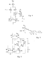
- FIG. 4 represents a conventional way of producing the charging and discharging current sources Ic, Id of the identification circuits of FIGS. 1 and 2.
- the sign indication outputs P and N of the comparator 10 of the preceding figures are applied at the inputs of a differential stage with two PNP transistors Q1 and Q2.
- the emitters of transistors Q1 and Q2 are charged by a constant current source 1 connected to the voltage Vcc.
- Source 1 is further activated by the signal BG of burst window.
- the transistor Q1 receives on its base the signal P and its collector is connected to the input of a current mirror formed of NPN transistors Q3 and Q4.
- the transistor Q3 is connected as a diode, that is to say that its collector and its base are connected together.
- the collector and the base of transistor Q3 form the input of the mirror and are connected to the base of transistor Q4.
- the collector of transistor Q4 forms the output of the mirror.
- the emitters of the transistors Q3 and Q4 are connected to ground.
- the transistor Q2 receives on its base the signal N and its collector is connected to the input of a mirror formed by NPN transistors Q5 and Q6 connected in the same way as the transistors Q3 and Q4, the transistor Q5 being that connected in diode.
- the collector of transistor Q6 is connected to the voltage Vcc and the emitters of transistors Q5 and Q6 are connected to the collector of transistor Q4 and to the terminal Ade of capacitance C.
- the mirror Q3, Q4 is a mirror multiplied by a factor n + 1 and the mirror Q5, Q6 is a mirror multiplying by a factor n. This is obtained by appropriately choosing the surfaces of the transistors Q3 to Q6.
- FIG. 5 shows inside a dotted frame an embodiment of the device according to the invention allowing, in the circuit of Figure 4, to increase the discharge current of the capacitance C by a constant factor when the voltage VA across the capacitance C becomes greater than a value Vo substantially equal to Vref.
- This device comprises a differential stage with two NPN transistors Q7 and Q8. The emitters of transistors Q7 and Q8 are connected to the collector of an NPN transistor Q9 connected in parallel on the base and the emitter of transistor Q4. The surface ratio between the transistors Q9 and Q3 is equal to m. With this configuration, the transistor Q9 serves as current source supplying a current equal to the collector current of transistor Q3 multiplied by m.
- the base of transistor Q7 receives the voltage Vo and the collector of transistor Q7 is connected to the voltage Vcc.
- the collector of transistor Q8 is connected to terminal A of capacitance C.
- Transistor Q8 is mounted in Darlington with a transistor Q10 whose base is connected to terminal A and whose collector is connected to voltage Vcc. With this configuration, when the voltage on terminal A is less than Vo + Vbe (Vbe designating the base-emitter voltage of transistor Q10), transistor Q7 is on and transistor Q8 is blocked. Then, transistor Q7 derives the entire collector current from transistor Q9. Under these conditions, the operation of the circuit is the same as that of FIG. 3.
- the sign indications provided by the comparator 10 are substantially random, and the number of positive indications is equal to the number of negative indications over a long period of time. .
- the number of positive indications is sufficiently greater than the number of negative indications for the voltage VA to reach the detection threshold Vref + Vt.
- FIG. 6 shows what would happen in such a case.
- This figure shows the evolution of the voltage VA when the standard received is good and when the initial state of the flip-flop 14 is initially wrong.
- the voltage VA begins by decreasing in stages and reaches the threshold Vref-Vt, for example at an instant t3 where the voltage VAa a value close to the value of the previous stage.
- the reset time signal R is activated and the flip-flop 14 remains in its state from time t3 to the start t4 of the next stage transition phase.
- the voltage VA increases, but does not again cross the threshold Vref-Vt, which is quite possible since the charge current is lower than the discharge current.
- the signal R remains active and the flip-flop 14 remains in the same state at the start t5 of the next transition phase.
- the voltage VA decreases ...
- the voltage VA can no longer cross the threshold Vref-Vt and it will never be detected that the standard received is the right one.
- the base of transistor Q8 can be directly connected to terminal A of capacitor C.
- Voltage Vo can have any value close to Vref.
- the charge current will be increased compared to the discharge current if the standard detection threshold is the low threshold Vref-Vt.
Landscapes
- Engineering & Computer Science (AREA)
- Multimedia (AREA)
- Signal Processing (AREA)
- Processing Of Color Television Signals (AREA)
- Color Television Systems (AREA)
- Manipulation Of Pulses (AREA)
Applications Claiming Priority (2)
| Application Number | Priority Date | Filing Date | Title |
|---|---|---|---|
| FR9211554 | 1992-09-18 | ||
| FR9211554A FR2696068B1 (fr) | 1992-09-18 | 1992-09-18 | Circuit d'identification de standard télévisé. |
Publications (2)
| Publication Number | Publication Date |
|---|---|
| EP0594512A1 true EP0594512A1 (de) | 1994-04-27 |
| EP0594512B1 EP0594512B1 (de) | 1997-11-12 |
Family
ID=9433970
Family Applications (1)
| Application Number | Title | Priority Date | Filing Date |
|---|---|---|---|
| EP93420370A Expired - Lifetime EP0594512B1 (de) | 1992-09-18 | 1993-09-16 | Schaltung zur Erkennung von Fernsehstandards |
Country Status (5)
| Country | Link |
|---|---|
| US (1) | US5400078A (de) |
| EP (1) | EP0594512B1 (de) |
| JP (1) | JPH06225313A (de) |
| DE (1) | DE69315173T2 (de) |
| FR (1) | FR2696068B1 (de) |
Cited By (1)
| Publication number | Priority date | Publication date | Assignee | Title |
|---|---|---|---|---|
| EP0710037A1 (de) * | 1994-10-31 | 1996-05-01 | STMicroelectronics S.A. | Farbfernsehstandarddetektor mit niedriger Empfangsschwelle |
Families Citing this family (4)
| Publication number | Priority date | Publication date | Assignee | Title |
|---|---|---|---|---|
| DE19619596B4 (de) * | 1996-05-15 | 2006-07-06 | Philips Intellectual Property & Standards Gmbh | Schaltungsanordnung zur Erkennung eines Farbbildsignals der SECAM-Übertragungsnorm |
| US5920353A (en) * | 1996-12-03 | 1999-07-06 | St Microelectronics, Inc. | Multi-standard decompression and/or compression device |
| US6028635A (en) * | 1996-12-03 | 2000-02-22 | Stmicroelectronics, Inc. | Reducing the memory required for decompression by storing compressed information using DCT based techniques |
| US6366327B1 (en) * | 1997-12-22 | 2002-04-02 | Texas Instruments Incorporated | Vertical sync detection and output for video decoder |
Citations (1)
| Publication number | Priority date | Publication date | Assignee | Title |
|---|---|---|---|---|
| EP0146777A1 (de) * | 1983-11-24 | 1985-07-03 | Motorola, Inc. | Anordnung zur Erkennung von PAL-SECAM |
Family Cites Families (4)
| Publication number | Priority date | Publication date | Assignee | Title |
|---|---|---|---|---|
| US4240102A (en) * | 1978-03-16 | 1980-12-16 | Rca Corporation | Identification system for SECAM or SECAM/PAL color television receivers |
| US4438451A (en) * | 1981-04-29 | 1984-03-20 | Rca Corporation | Dual-standard SECAM/PAL color TV receiver with automatic control of operating mode |
| FR2657804B1 (fr) * | 1990-02-05 | 1993-09-24 | Dimeco Enona | Bride de serrage autonome, a gaz, pour pieces diverses. |
| EP0562415A1 (de) * | 1992-03-25 | 1993-09-29 | THOMSON multimedia | Schaltungsanordnung zur Umschaltung zwischen PAL und SECAM in einem Fernsehempfänger |
-
1992
- 1992-09-18 FR FR9211554A patent/FR2696068B1/fr not_active Expired - Fee Related
-
1993
- 1993-09-16 JP JP5252136A patent/JPH06225313A/ja not_active Withdrawn
- 1993-09-16 DE DE69315173T patent/DE69315173T2/de not_active Expired - Fee Related
- 1993-09-16 EP EP93420370A patent/EP0594512B1/de not_active Expired - Lifetime
- 1993-09-16 US US08/122,373 patent/US5400078A/en not_active Expired - Lifetime
Patent Citations (1)
| Publication number | Priority date | Publication date | Assignee | Title |
|---|---|---|---|---|
| EP0146777A1 (de) * | 1983-11-24 | 1985-07-03 | Motorola, Inc. | Anordnung zur Erkennung von PAL-SECAM |
Non-Patent Citations (1)
| Title |
|---|
| IEEE TRANSACTIONS ON CONSUMER ELECTRONICS vol. 31, no. 3, Août 1985, NEW YORK, US pages 147 - 155 PERY ET AL 'a fully automatic multistandard tv chrominance decoder' * |
Cited By (2)
| Publication number | Priority date | Publication date | Assignee | Title |
|---|---|---|---|---|
| EP0710037A1 (de) * | 1994-10-31 | 1996-05-01 | STMicroelectronics S.A. | Farbfernsehstandarddetektor mit niedriger Empfangsschwelle |
| FR2726423A1 (fr) * | 1994-10-31 | 1996-05-03 | Sgs Thomson Microelectronics | Detecteur de norme de television couleur a faible seuil de reception |
Also Published As
| Publication number | Publication date |
|---|---|
| FR2696068A1 (fr) | 1994-03-25 |
| DE69315173T2 (de) | 1998-03-12 |
| FR2696068B1 (fr) | 1994-12-30 |
| JPH06225313A (ja) | 1994-08-12 |
| US5400078A (en) | 1995-03-21 |
| DE69315173D1 (de) | 1997-12-18 |
| EP0594512B1 (de) | 1997-11-12 |
Similar Documents
| Publication | Publication Date | Title |
|---|---|---|
| EP0408436B1 (de) | Detektionsschaltung für ein Drehstromgenerator-Überwachungssignal eines Reglers zum Laden der Batterie eines Kraftfahrzeuges und seine Verwendung | |
| EP0421897B1 (de) | Vorrichtung zum Extrahieren von digitalen Daten aus einem Video-Signal | |
| FR2473239A1 (fr) | Televiseur avec circuit generateur de retard | |
| EP0594512B1 (de) | Schaltung zur Erkennung von Fernsehstandards | |
| EP0115234A1 (de) | Verfahren und Schaltung zur Frequenz- und Phasenverkopplung eines örtlichen Oszillators im Fernsehen | |
| EP0323935B1 (de) | Schaltung zur Erkennung eines Videorecordersignals | |
| EP0329576B1 (de) | Erkennungsschaltung zur Zeilensynchronisierung | |
| FR2550028A1 (fr) | Circuit d'alimentation delivrant des tensions continues d'egale grandeur mais de polarite opposee, notamment pour appareils de reproduction sonore a bord d'automobiles | |
| FR3131787A1 (fr) | Carte sans contact téléalimentée | |
| EP0441723B1 (de) | Automatisches Verfahren zur Farbfernsehnormidentifizierung | |
| EP0625849B1 (de) | Schaltungsanordnung zum Einstellen des Schwarzwertes eines Videosignals | |
| EP0478473B1 (de) | Secam Decoder | |
| WO1994030005A1 (fr) | Dispositif d'extraction de synchronisation d'un signal video | |
| FR2494948A1 (fr) | Generateur de signaux composes de temporisation ayant un niveau previsible de sortie | |
| EP0722217B1 (de) | Vorrichtung zur Einstellung der Dämpfung eines Signals | |
| EP0952740B1 (de) | Demodulator, insbesondere von SECAM-Chrominanzsignal, mit Frequenzdoppelabstimmungsvorrichtung | |
| FR2571577A1 (fr) | Systeme de controle de surcharge de chrominance | |
| EP0488457B1 (de) | Vorrichtung zum Klemmen eines Grundbandsignals | |
| FR2778053A1 (fr) | Demodulateur de signal de chrominance secam a deux voies rouge>bleu et a oscillateur unique | |
| JPH0654244A (ja) | ビデオカメラの電子シャッタ | |
| FR2516734A1 (fr) | Generateur d'impulsions de declenchement de la composante de synchronisation de sous-porteuse de chrominance et de blocage du palier arriere | |
| FR2612719A1 (fr) | Circuit de balayage ligne et de generation de tension | |
| FR2762743A1 (fr) | Procede et dispositif de detection de la norme de transmission d'un signal d'image couleur | |
| FR2551297A1 (fr) | Dispositif de production d'impulsions de verrouillage d'une porte d'un signal de synchronisation de sous-porteuse de chrominance de largeur constante | |
| FR2843267A1 (fr) | Procede et circuit de fourniture d'un signal de balayage horizontal pour televiseur |
Legal Events
| Date | Code | Title | Description |
|---|---|---|---|
| PUAI | Public reference made under article 153(3) epc to a published international application that has entered the european phase |
Free format text: ORIGINAL CODE: 0009012 |
|
| AK | Designated contracting states |
Kind code of ref document: A1 Designated state(s): DE FR GB IT |
|
| 17P | Request for examination filed |
Effective date: 19941005 |
|
| GRAG | Despatch of communication of intention to grant |
Free format text: ORIGINAL CODE: EPIDOS AGRA |
|
| 17Q | First examination report despatched |
Effective date: 19970109 |
|
| GRAH | Despatch of communication of intention to grant a patent |
Free format text: ORIGINAL CODE: EPIDOS IGRA |
|
| GRAH | Despatch of communication of intention to grant a patent |
Free format text: ORIGINAL CODE: EPIDOS IGRA |
|
| GRAA | (expected) grant |
Free format text: ORIGINAL CODE: 0009210 |
|
| AK | Designated contracting states |
Kind code of ref document: B1 Designated state(s): DE FR GB IT |
|
| GBT | Gb: translation of ep patent filed (gb section 77(6)(a)/1977) |
Effective date: 19971119 |
|
| REF | Corresponds to: |
Ref document number: 69315173 Country of ref document: DE Date of ref document: 19971218 |
|
| ITF | It: translation for a ep patent filed | ||
| PLBE | No opposition filed within time limit |
Free format text: ORIGINAL CODE: 0009261 |
|
| STAA | Information on the status of an ep patent application or granted ep patent |
Free format text: STATUS: NO OPPOSITION FILED WITHIN TIME LIMIT |
|
| 26N | No opposition filed | ||
| REG | Reference to a national code |
Ref country code: GB Ref legal event code: IF02 |
|
| PGFP | Annual fee paid to national office [announced via postgrant information from national office to epo] |
Ref country code: DE Payment date: 20020925 Year of fee payment: 10 |
|
| PG25 | Lapsed in a contracting state [announced via postgrant information from national office to epo] |
Ref country code: DE Free format text: LAPSE BECAUSE OF NON-PAYMENT OF DUE FEES Effective date: 20040401 |
|
| PGFP | Annual fee paid to national office [announced via postgrant information from national office to epo] |
Ref country code: FR Payment date: 20040908 Year of fee payment: 12 |
|
| PGFP | Annual fee paid to national office [announced via postgrant information from national office to epo] |
Ref country code: GB Payment date: 20040915 Year of fee payment: 12 |
|
| PG25 | Lapsed in a contracting state [announced via postgrant information from national office to epo] |
Ref country code: IT Free format text: LAPSE BECAUSE OF NON-PAYMENT OF DUE FEES Effective date: 20050916 Ref country code: GB Free format text: LAPSE BECAUSE OF NON-PAYMENT OF DUE FEES Effective date: 20050916 |
|
| GBPC | Gb: european patent ceased through non-payment of renewal fee |
Effective date: 20050916 |
|
| PG25 | Lapsed in a contracting state [announced via postgrant information from national office to epo] |
Ref country code: FR Free format text: LAPSE BECAUSE OF NON-PAYMENT OF DUE FEES Effective date: 20060531 |
|
| REG | Reference to a national code |
Ref country code: FR Ref legal event code: ST Effective date: 20060531 |