EP0594878A1 - Système de télécommunication optique passif - Google Patents
Système de télécommunication optique passif Download PDFInfo
- Publication number
- EP0594878A1 EP0594878A1 EP92118260A EP92118260A EP0594878A1 EP 0594878 A1 EP0594878 A1 EP 0594878A1 EP 92118260 A EP92118260 A EP 92118260A EP 92118260 A EP92118260 A EP 92118260A EP 0594878 A1 EP0594878 A1 EP 0594878A1
- Authority
- EP
- European Patent Office
- Prior art keywords
- bit
- clock
- register
- byte
- reset
- Prior art date
- Legal status (The legal status is an assumption and is not a legal conclusion. Google has not performed a legal analysis and makes no representation as to the accuracy of the status listed.)
- Granted
Links
- 230000003287 optical effect Effects 0.000 title claims description 12
- 230000015654 memory Effects 0.000 claims description 8
- 230000001360 synchronised effect Effects 0.000 claims description 7
- 230000002123 temporal effect Effects 0.000 claims description 4
- 239000000835 fiber Substances 0.000 description 11
- 239000013307 optical fiber Substances 0.000 description 10
- 230000005540 biological transmission Effects 0.000 description 7
- 230000004913 activation Effects 0.000 description 6
- 230000008054 signal transmission Effects 0.000 description 6
- 238000006243 chemical reaction Methods 0.000 description 4
- 238000001514 detection method Methods 0.000 description 4
- 238000004891 communication Methods 0.000 description 3
- 230000006978 adaptation Effects 0.000 description 2
- 230000002457 bidirectional effect Effects 0.000 description 2
- 238000000034 method Methods 0.000 description 2
- 230000002441 reversible effect Effects 0.000 description 2
- 238000000926 separation method Methods 0.000 description 2
- 230000003111 delayed effect Effects 0.000 description 1
- 238000011161 development Methods 0.000 description 1
- 230000018109 developmental process Effects 0.000 description 1
- 238000005516 engineering process Methods 0.000 description 1
- 230000006870 function Effects 0.000 description 1
- 238000002372 labelling Methods 0.000 description 1
- 230000001404 mediated effect Effects 0.000 description 1
- 238000005070 sampling Methods 0.000 description 1
- 230000001960 triggered effect Effects 0.000 description 1
- 238000011144 upstream manufacturing Methods 0.000 description 1
Images
Classifications
-
- H—ELECTRICITY
- H04—ELECTRIC COMMUNICATION TECHNIQUE
- H04Q—SELECTING
- H04Q11/00—Selecting arrangements for multiplex systems
- H04Q11/04—Selecting arrangements for multiplex systems for time-division multiplexing
- H04Q11/0428—Integrated services digital network, i.e. systems for transmission of different types of digitised signals, e.g. speech, data, telecentral, television signals
- H04Q11/0478—Provisions for broadband connections
-
- H—ELECTRICITY
- H04—ELECTRIC COMMUNICATION TECHNIQUE
- H04L—TRANSMISSION OF DIGITAL INFORMATION, e.g. TELEGRAPHIC COMMUNICATION
- H04L7/00—Arrangements for synchronising receiver with transmitter
- H04L7/0008—Synchronisation information channels, e.g. clock distribution lines
- H04L7/0012—Synchronisation information channels, e.g. clock distribution lines by comparing receiver clock with transmitter clock
-
- H—ELECTRICITY
- H04—ELECTRIC COMMUNICATION TECHNIQUE
- H04L—TRANSMISSION OF DIGITAL INFORMATION, e.g. TELEGRAPHIC COMMUNICATION
- H04L7/00—Arrangements for synchronising receiver with transmitter
- H04L7/0016—Arrangements for synchronising receiver with transmitter correction of synchronization errors
- H04L7/005—Correction by an elastic buffer
-
- H—ELECTRICITY
- H04—ELECTRIC COMMUNICATION TECHNIQUE
- H04L—TRANSMISSION OF DIGITAL INFORMATION, e.g. TELEGRAPHIC COMMUNICATION
- H04L7/00—Arrangements for synchronising receiver with transmitter
- H04L7/04—Speed or phase control by synchronisation signals
- H04L7/041—Speed or phase control by synchronisation signals using special codes as synchronising signal
- H04L2007/045—Fill bit or bits, idle words
-
- H—ELECTRICITY
- H04—ELECTRIC COMMUNICATION TECHNIQUE
- H04L—TRANSMISSION OF DIGITAL INFORMATION, e.g. TELEGRAPHIC COMMUNICATION
- H04L12/00—Data switching networks
- H04L12/54—Store-and-forward switching systems
- H04L12/56—Packet switching systems
- H04L12/5601—Transfer mode dependent, e.g. ATM
- H04L2012/5603—Access techniques
- H04L2012/5609—Topology
- H04L2012/561—Star, e.g. cross-connect, concentrator, subscriber group equipment, remote electronics
-
- H—ELECTRICITY
- H04—ELECTRIC COMMUNICATION TECHNIQUE
- H04L—TRANSMISSION OF DIGITAL INFORMATION, e.g. TELEGRAPHIC COMMUNICATION
- H04L12/00—Data switching networks
- H04L12/54—Store-and-forward switching systems
- H04L12/56—Packet switching systems
- H04L12/5601—Transfer mode dependent, e.g. ATM
- H04L2012/5672—Multiplexing, e.g. coding, scrambling
-
- H—ELECTRICITY
- H04—ELECTRIC COMMUNICATION TECHNIQUE
- H04L—TRANSMISSION OF DIGITAL INFORMATION, e.g. TELEGRAPHIC COMMUNICATION
- H04L7/00—Arrangements for synchronising receiver with transmitter
- H04L7/04—Speed or phase control by synchronisation signals
Definitions
- B-ISDN integrated services digital networks
- LWL optical fibers
- EP-A2-0 171 080 optical fibers communication networks
- CCITT proposes an interface (T B or V B interface) with a transmission capacity of 155.52 Mbit / s for a fiber optic connection - a bit rate that at least for the foreseeable future a majority of the participants, both privately and is far from being exploited in the business field.
- a passive optical telecommunication system in the subscriber line, in which in each case a plurality of subscriber stations is connected via a separate optical fiber subscriber line to a passive optical fiber splitter, which is connected directly or via at least one additional passive one optical fiber splitter is connected to a common optical fiber connection of the exchange via an optical fiber bus, in which the signal transmission from the switching center to the subscriber stations takes place in an ATM cell stream, from which each subscriber station only accepts the ATM cells provided in the cell header with an identifier assigned to this subscriber station, and in which the signal transmission from the subscriber stations to the exchange takes place in a TDMA process with ATM cells, consequently a subscriber station only receives an ATM after receiving a permit (e.g.
- Cell can send out after such a delay time measured individually for the subscriber, which is determined by the running time of the recorded ATM cell and the running time of the sent ATM cell at a predetermined loop running time, which is the same for all subscriber stations, between the transmission of an ATM cell picked up by the subscriber station concerned the switching center and the reception of the ATM cell subsequently sent out by the relevant subscriber station by the switching center.
- the switching center repeatedly sets a programmable digital delay device in the decentralized device in accordance with the loop running time between the decentralized device and the switching center with regard to the uniform loop running time and the decentralized device with each burst With the help of the delay device set individually by the switching center, in such a way that that the decentralized device generates the burst after only one - in the event of a gap of (on average) two bits between two successive ATM cells in the switching center from the decentralized devices received ATM cell sequence with an accuracy of ⁇ 1 bit - coarse delay time of one or more whole system clock periods before the transmission time required for a desired reception phase position of the burst in the switching center and that only the switching center centrally sends a fine-tuning of the bursts arriving at it to the device the desired reception phase position.
- the switching center then presents itself as a system in which a digital signal is received serially and block by block with a constant clock, but with a different phase position from block to block, and in which the individual digital signal blocks therefore first of all to their own system clock (official clock) synchronized or, in other words, must be taken over with the official clock; then all received digital signal blocks can then be further processed (in particular processed, mediated or transmitted) in the official clock, with signal processing also being made possible by correspondingly slower ICs by means of a digital signal parallelization to be carried out after the block frame position has been determined.
- official clock system clock
- the invention now shows a way to a particularly low-cost implementation of clock adaptation, block frame detection and parallelization.
- the invention relates to a circuit arrangement for the acceptance of n-digit n-bit words with the official bit clock, each received serially in a line bit clock and to be passed on in parallel in accordance with an official clock, hereinafter referred to generally as bytes, with the official bit clock, each with a serial n- bit word (byte) described in the line bit clock and FIFO memory to be read out in each case in the official bit clock, in particular for taking over ATM cells received from decentralized devices in the switching center of a passive optical telecommunications network;
- This circuit arrangement is characterized according to the invention in that the bit storage locations of the first n-bit register of two n-bit registers, which are cyclically driven on the input side in the line bit cycle, on the output side lead to the inputs of the bit storage locations of the second n-bit register cyclically driven in the official bit cycle on the input side, and in that a byte boundary detector determines the beginning of a subsequent byte on the basis of an identification bit pattern contained in the received bit stream
- control of the first n-bit register can also be reset by a (modulo n) counter which is switched on with the line bit clock and reset by the byte limit detector and the control of the second n-bit register reset by a (modulo n) counter switched on with the external bit clock and reset by the byte limit detector via a delay element synchronous to the output clock synchronized with the output clock when the counter is reset.
- the invention has the advantage of a low-effort combination of clock adaptation and parallelization of the digital signal.
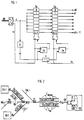
- FIG 1 is a circuit arrangement for taking over ATM cells received from decentralized devices in a central device (switching center) of a passive optical device, to the extent necessary for understanding the invention
- Telecommunications system shown as it is schematically outlined in FIG 2.
- FIG. 2 it is a bidirectional FO telecommunication system with a passive (preferably single-mode) FO bus network, which is located between a central telecommunication device CU, for example a switching center, and a plurality of decentralized telecommunication devices ..., DU2, DU3, ..., e.g. subscriber positions or so-called distant units.
- the decentralized telecommunication devices DU are connected to a common fiber optic multiplex connection of the central telecommunication device CU via a single or multi-fiber optical fiber bus OB;
- the fiber optic connection lines OAL1, ..., OALn may be connected to the associated fiber optic bus OB via passive, ie not wavelength-selective, optical fiber splitters V1, ... Vn, either directly, as explicitly shown in FIG. 2, or also via other such branching devices.
- Continuous mixers or optical directional couplers, for example, can be used as optical splitters. It is also possible to provide a common optical splitter for a plurality of fiber optic connecting lines, as is known per se (for example from EP-A2-0 171 080) and therefore need not be described in more detail here.
- a wavelength separation operation can be provided for directional separation, in that light of a first wavelength, for example in the 1550 nm band, is used for signal transmission in the downward direction from the central telecommunications device CU to the decentralized telecommunications devices DU Signal transmission in the upward direction from the decentralized telecommunication devices ..., DU2, DU3, ... to the central telecommunication device CU light of a somewhat smaller one, for example second wavelength lying in the 1300 nm band is used.
- a first wavelength for example in the 1550 nm band
- a corresponding electro-optical converter expediently formed by a laser diode and a corresponding opto-electrical converter, expediently formed by an avalanche or PIN photodiode, can be provided in the central telecommunication device, which are connected to the associated optical fiber bus OB via a wavelength-selective optical filter, for example a (for example from US-A-4 790 616) known optical switch module provided with an interference beam splitter are connected.
- the decentralized telecommunication devices ..., DU2, DU3, ... may also be provided with electro-optical and opto-electrical converters.
- the invention can of course also be used if, in deviation from the graphic representation, a separate fiber is provided for the downstream traffic and for the upstream traffic.
- each ATM cell comprising 53 bit octets and consisting of a (5 octet) control information field (header) and a (48 octet) useful information field may have an overhead of equal length in both directions added, in the downward direction a pure preamble, in the upward direction a transmission gap to the ATM cell preceding on the FO bus OB and a correspondingly shorter preamble.
- a (5 octet) control information field (header) and a (48 octet) useful information field may have an overhead of equal length in both directions added, in the downward direction a pure preamble, in the upward direction a transmission gap to the ATM cell preceding on the FO bus OB and a correspondingly shorter preamble.
- Synchronization cells can also be used in the ATM cell stream Z down if no user information is to be transmitted predefined bit pattern for synchronizing the decentralized devices with the respective cell start (so-called pure ATM); however, it is also possible for the ATM cell stream Z down to be embedded in a (for example STM-1) time frame structure with synchronization signals (overhead) which occur at certain fixed intervals (so-called frame structured ATM).
- each decentralized device DU takes only those ATM cells which, in their header, preferably in its virtual path identifier, with (one) this decentralized device DU or the subscriber (s) connected to it ( n) assigned labeling (s) are addressed.
- a decentralized device DU can in turn only deliver an ATM cell after receiving a corresponding permission, for example with an ATM cell of the ATM cell stream Z down , which is addressed to it, and specifically according to a DU dimensioned individually Delay Time.
- This delay time is dimensioned such that it changes with the running time t down of the ATM cells from the central device CU to the relevant decentralized device DU and the running time t up from the relevant decentralized device DU to the central device CU to one for all decentralized devices ..., DU2, DU3, ... same predetermined loop running time between the sending out of an ATM cell to be taken up by the relevant decentralized device DU by the central device CU and the reception of the ATM cell subsequently transmitted by the relevant decentralized device DU added by the central device CU.
- the ATM cells forming the upward burst current Z up are not only reserved in one at a time Transmitted time slot, but that they can be taken over within this time slot with a desired optimal reception phase position, namely with the official clock of the central device CU.
- the decentralized devices DU ATM cells each after only one - with a gap of (on average) two bits between two successive ATM cells of the ATM cell sequence received in the central device from the decentralized devices send rough delay time of one or more whole system clock periods transmission time required before the desired for a receiving phase position of the ATM cells in the central unit CU and that only the central unit CU centrally a respective DU individually sized fine delay of at it - to ⁇ 1 bit exact incoming ATM cells.
- the central device CU can be provided on the input side with a takeover circuit downstream of its optoelectrical converter o / e for taking over n-digit bytes, each received serially in a line bit cycle and to be passed on in parallel in accordance with an office cycle, as shown schematically in FIG 1 is shown.
- this circuit arrangement has two n-bit registers Se, Sa, each with n bit memory locations 0.1,... N-1.
- the n bit memory locations of the first n-bit register Se are connected on the input side to an input signal line e which carries the received signal converted in the optoelectric converter o / e from optical to electrical (ATM cell sequence Z up in FIG. 1) and are connected by one to that of the electro-optical converter o / e obtained input signal bit clock (line bit clock) leading line bit clock line te her unlocked cyclically, so that in each case n on the input signal line e serially occurring bits reach the n bit memory locations 0,1, ... n-1 of the first n-bit register Se.
- the n bit storage locations 0.1, ... n-1 of the first n-bit register Se lead to the inputs of the n bit storage locations 0.1, ... .n-1 of the second n-bit register Sa, which of an external bit clock line ta leading the central bit clock of the central device CU in FIG. 2 is cyclically driven so that the n bits just stored in the first n bit register Se are successively transferred to the n bit memory locations 0.1,... n. 1 of the second n register Sa arrive.
- a byte limit detector D which is also connected on the input side to the input signal line e, can be formed by a block frame position detector, which detects an identifier bit pattern contained in the received bit stream, in particular in the form of a so-called cell delineation identification (CDI), and the start of a subsequent one, here generally as a byte recognizes the designated n-bit word, on the temporal position of which the first n-bit register Se is synchronized.
- CDI cell delineation identification
- the reset signal emitted by the byte limit detector D is also delayed by about half a byte length of the reset input of a second (modulo n) via an at least output-side digital delay element V, which is synchronous with the office clock, which can be implemented in the form of an office bit clock-controlled (n / 2) -bit shift register.
- Counter Za supplied. This second (modulo n) counter Za is synchronized with the cyclical activation of the second n-bit register Sa with the external bit clock (ta) of the central device (CU in FIG. 2).
- the second (modulo n) counter Za also resets the activation of the second n-bit register Sa to the start of a new activation cycle.
- the byte bit by bit which has just arrived as a whole byte in the first n-bit register Se, also now as a whole byte in the official bit clock (ta) in the second n-bit Register Sa is taken over, after which it is available at its parallel outputs p0, p1 ...., p (n-1) for forwarding in parallel.
- the (CDI) identifier bit pattern does not end at a byte boundary, but in the mth bit of a byte, then the (modulo n) counter Za is not on the zeroth but on the (m + 1) th counting step reset; the same applies to the n-bit register Sa.
- the counter readings of the two (modulo n) counters Ze and Za are always at a distance of about n / 2 due to the specified reset delay, so that a simultaneous Write and read access to one and the same bit storage space of the n-bit register Se is avoided.
Landscapes
- Engineering & Computer Science (AREA)
- Computer Networks & Wireless Communication (AREA)
- Signal Processing (AREA)
- Data Exchanges In Wide-Area Networks (AREA)
- Optical Communication System (AREA)
- Synchronisation In Digital Transmission Systems (AREA)
- Exchange Systems With Centralized Control (AREA)
Priority Applications (3)
| Application Number | Priority Date | Filing Date | Title |
|---|---|---|---|
| AT92118260T ATE170350T1 (de) | 1992-10-26 | 1992-10-26 | Passives optisches telekommunikationssystem |
| DE59209472T DE59209472D1 (de) | 1992-10-26 | 1992-10-26 | Passives optisches Telekommunikationssystem |
| EP92118260A EP0594878B1 (fr) | 1992-10-26 | 1992-10-26 | Système de télécommunication optique passif |
Applications Claiming Priority (1)
| Application Number | Priority Date | Filing Date | Title |
|---|---|---|---|
| EP92118260A EP0594878B1 (fr) | 1992-10-26 | 1992-10-26 | Système de télécommunication optique passif |
Publications (2)
| Publication Number | Publication Date |
|---|---|
| EP0594878A1 true EP0594878A1 (fr) | 1994-05-04 |
| EP0594878B1 EP0594878B1 (fr) | 1998-08-26 |
Family
ID=8210176
Family Applications (1)
| Application Number | Title | Priority Date | Filing Date |
|---|---|---|---|
| EP92118260A Expired - Lifetime EP0594878B1 (fr) | 1992-10-26 | 1992-10-26 | Système de télécommunication optique passif |
Country Status (3)
| Country | Link |
|---|---|
| EP (1) | EP0594878B1 (fr) |
| AT (1) | ATE170350T1 (fr) |
| DE (1) | DE59209472D1 (fr) |
Cited By (1)
| Publication number | Priority date | Publication date | Assignee | Title |
|---|---|---|---|---|
| EP2019501B1 (fr) * | 2007-07-24 | 2011-01-05 | Alcatel Lucent | Procédé et dispositif pour détecter le démarrage de paquets de données en mode rafale |
Citations (3)
| Publication number | Priority date | Publication date | Assignee | Title |
|---|---|---|---|---|
| EP0231590A2 (fr) * | 1986-01-22 | 1987-08-12 | Nortel Networks Corporation | Alignement de trame des signaux subordonnés d'un courant de bits à multiplexage temporel par répartition |
| EP0383557A1 (fr) * | 1989-02-16 | 1990-08-22 | BRITISH TELECOMMUNICATIONS public limited company | Synchronisation d'horloge de réseau |
| EP0488572A2 (fr) * | 1990-11-28 | 1992-06-03 | AT&T Corp. | Appareil pour l'alignement de la phase |
-
1992
- 1992-10-26 AT AT92118260T patent/ATE170350T1/de not_active IP Right Cessation
- 1992-10-26 EP EP92118260A patent/EP0594878B1/fr not_active Expired - Lifetime
- 1992-10-26 DE DE59209472T patent/DE59209472D1/de not_active Expired - Fee Related
Patent Citations (3)
| Publication number | Priority date | Publication date | Assignee | Title |
|---|---|---|---|---|
| EP0231590A2 (fr) * | 1986-01-22 | 1987-08-12 | Nortel Networks Corporation | Alignement de trame des signaux subordonnés d'un courant de bits à multiplexage temporel par répartition |
| EP0383557A1 (fr) * | 1989-02-16 | 1990-08-22 | BRITISH TELECOMMUNICATIONS public limited company | Synchronisation d'horloge de réseau |
| EP0488572A2 (fr) * | 1990-11-28 | 1992-06-03 | AT&T Corp. | Appareil pour l'alignement de la phase |
Cited By (1)
| Publication number | Priority date | Publication date | Assignee | Title |
|---|---|---|---|---|
| EP2019501B1 (fr) * | 2007-07-24 | 2011-01-05 | Alcatel Lucent | Procédé et dispositif pour détecter le démarrage de paquets de données en mode rafale |
Also Published As
| Publication number | Publication date |
|---|---|
| DE59209472D1 (de) | 1998-10-01 |
| EP0594878B1 (fr) | 1998-08-26 |
| ATE170350T1 (de) | 1998-09-15 |
Similar Documents
| Publication | Publication Date | Title |
|---|---|---|
| EP0460398B1 (fr) | Système de télécommunication optique passif | |
| DE3882922T2 (de) | Verwürfelung in einem digitalen Uebertragungsnetzwerk. | |
| DE69534445T2 (de) | Verfahren zur TDMA-Verwaltung, Zentralstation, Teilnehmerstation und Netzwerk zur Ausführung des Verfahrens | |
| DE60001046T2 (de) | Verfahren und Vorrichtung zur TDM/TDMA-Kommunikation | |
| DE69425585T2 (de) | Passives optisches netzwerk für video auf abruf | |
| EP0673166B1 (fr) | Méthode de récupération d'horloge dans un récepteur pour des signaux vidéo transmis numeriquement en mode ATM dans des réseaux coaxial/fibre optique d'abbonés | |
| DE69725718T2 (de) | Verfahren zur strukturierung digitaler daten, die in beiden richtungen eines passiven optischen netzwerks eines pon-tdma-systems übertragbar sind | |
| EP0171080B1 (fr) | Système de télécommunications à services intégrés pour services à bande étroite | |
| EP0291135B1 (fr) | Etage de concentration pour un système de commutation à large bande | |
| EP0256027B1 (fr) | Procede permettant le fonctionnement simultane de plusieurs terminaux sur un bloc de raccordement d'un reseau a large bande | |
| DE4123851C1 (en) | Inter-working unit for coupling asynchronous-to synchronous-transfer mode network - uses multiplexer and demultiplexer for each network, buffer memory and asynchronous-synchronous converters for transmission via exchanges | |
| EP0284106B1 (fr) | Dispositif pour intercaler une voie de service pour un système de transmission | |
| EP0425732A1 (fr) | Système optique passif de télécommunication | |
| EP0587930B1 (fr) | Procédé de commutation pour des cellules de communication optiques | |
| DE69023344T2 (de) | Optisches Schaltungsnetz. | |
| EP0594878B1 (fr) | Système de télécommunication optique passif | |
| DE4008729C2 (fr) | ||
| DE4233581C2 (de) | Rahmenaufbau für ein Telekommunikationssystem mit optischer Digitalsignal-Übertragung | |
| EP0632942B1 (fr) | Procede de repartition d'intervalles de temps de transmission dans un reseau optique passif | |
| EP0126413B1 (fr) | Système de télécommunication à la fois pour trafic en mode-circuit et pour trafic en mode-paquet | |
| DE60034540T2 (de) | Teilnehmerbusleitung mit variabler Datenrate | |
| DE69534072T2 (de) | Anordnung und Verfahren zur Steuerung der Takt bei digitalen Datenübertragung in einem passiven optischen TDMA system | |
| DE4313388C1 (de) | Anschlußnetz in einem Kommunikationssystem | |
| DE68907973T2 (de) | Regenerierungsknoten für ein Übertragungsnetz. | |
| EP0472824A1 (fr) | Système de télécommunication optique passif |
Legal Events
| Date | Code | Title | Description |
|---|---|---|---|
| PUAI | Public reference made under article 153(3) epc to a published international application that has entered the european phase |
Free format text: ORIGINAL CODE: 0009012 |
|
| AK | Designated contracting states |
Kind code of ref document: A1 Designated state(s): AT BE CH DE FR GB IT LI NL SE |
|
| 17P | Request for examination filed |
Effective date: 19941020 |
|
| GRAG | Despatch of communication of intention to grant |
Free format text: ORIGINAL CODE: EPIDOS AGRA |
|
| 17Q | First examination report despatched |
Effective date: 19971020 |
|
| GRAG | Despatch of communication of intention to grant |
Free format text: ORIGINAL CODE: EPIDOS AGRA |
|
| GRAH | Despatch of communication of intention to grant a patent |
Free format text: ORIGINAL CODE: EPIDOS IGRA |
|
| GRAH | Despatch of communication of intention to grant a patent |
Free format text: ORIGINAL CODE: EPIDOS IGRA |
|
| GRAA | (expected) grant |
Free format text: ORIGINAL CODE: 0009210 |
|
| AK | Designated contracting states |
Kind code of ref document: B1 Designated state(s): AT BE CH DE FR GB IT LI NL SE |
|
| REF | Corresponds to: |
Ref document number: 170350 Country of ref document: AT Date of ref document: 19980915 Kind code of ref document: T |
|
| REG | Reference to a national code |
Ref country code: CH Ref legal event code: NV Representative=s name: SIEMENS SCHWEIZ AG Ref country code: CH Ref legal event code: EP |
|
| REF | Corresponds to: |
Ref document number: 59209472 Country of ref document: DE Date of ref document: 19981001 |
|
| GBT | Gb: translation of ep patent filed (gb section 77(6)(a)/1977) |
Effective date: 19981027 |
|
| ET | Fr: translation filed | ||
| PLBE | No opposition filed within time limit |
Free format text: ORIGINAL CODE: 0009261 |
|
| STAA | Information on the status of an ep patent application or granted ep patent |
Free format text: STATUS: NO OPPOSITION FILED WITHIN TIME LIMIT |
|
| 26N | No opposition filed | ||
| PGFP | Annual fee paid to national office [announced via postgrant information from national office to epo] |
Ref country code: AT Payment date: 20010926 Year of fee payment: 10 |
|
| PGFP | Annual fee paid to national office [announced via postgrant information from national office to epo] |
Ref country code: GB Payment date: 20011016 Year of fee payment: 10 |
|
| PGFP | Annual fee paid to national office [announced via postgrant information from national office to epo] |
Ref country code: SE Payment date: 20011018 Year of fee payment: 10 Ref country code: NL Payment date: 20011018 Year of fee payment: 10 |
|
| PGFP | Annual fee paid to national office [announced via postgrant information from national office to epo] |
Ref country code: BE Payment date: 20011024 Year of fee payment: 10 |
|
| PGFP | Annual fee paid to national office [announced via postgrant information from national office to epo] |
Ref country code: FR Payment date: 20011031 Year of fee payment: 10 |
|
| PGFP | Annual fee paid to national office [announced via postgrant information from national office to epo] |
Ref country code: DE Payment date: 20011217 Year of fee payment: 10 |
|
| REG | Reference to a national code |
Ref country code: GB Ref legal event code: IF02 |
|
| PGFP | Annual fee paid to national office [announced via postgrant information from national office to epo] |
Ref country code: CH Payment date: 20020110 Year of fee payment: 10 |
|
| PG25 | Lapsed in a contracting state [announced via postgrant information from national office to epo] |
Ref country code: GB Free format text: LAPSE BECAUSE OF NON-PAYMENT OF DUE FEES Effective date: 20021026 Ref country code: AT Free format text: LAPSE BECAUSE OF NON-PAYMENT OF DUE FEES Effective date: 20021026 |
|
| PG25 | Lapsed in a contracting state [announced via postgrant information from national office to epo] |
Ref country code: SE Free format text: LAPSE BECAUSE OF NON-PAYMENT OF DUE FEES Effective date: 20021027 |
|
| PG25 | Lapsed in a contracting state [announced via postgrant information from national office to epo] |
Ref country code: LI Free format text: LAPSE BECAUSE OF NON-PAYMENT OF DUE FEES Effective date: 20021031 Ref country code: CH Free format text: LAPSE BECAUSE OF NON-PAYMENT OF DUE FEES Effective date: 20021031 Ref country code: BE Free format text: LAPSE BECAUSE OF NON-PAYMENT OF DUE FEES Effective date: 20021031 |
|
| BERE | Be: lapsed |
Owner name: *SIEMENS A.G. Effective date: 20021031 |
|
| PG25 | Lapsed in a contracting state [announced via postgrant information from national office to epo] |
Ref country code: NL Free format text: LAPSE BECAUSE OF NON-PAYMENT OF DUE FEES Effective date: 20030501 Ref country code: DE Free format text: LAPSE BECAUSE OF NON-PAYMENT OF DUE FEES Effective date: 20030501 |
|
| EUG | Se: european patent has lapsed | ||
| REG | Reference to a national code |
Ref country code: CH Ref legal event code: PL |
|
| GBPC | Gb: european patent ceased through non-payment of renewal fee | ||
| PG25 | Lapsed in a contracting state [announced via postgrant information from national office to epo] |
Ref country code: FR Free format text: LAPSE BECAUSE OF NON-PAYMENT OF DUE FEES Effective date: 20030630 |
|
| NLV4 | Nl: lapsed or anulled due to non-payment of the annual fee |
Effective date: 20030501 |
|
| REG | Reference to a national code |
Ref country code: FR Ref legal event code: ST |
|
| PG25 | Lapsed in a contracting state [announced via postgrant information from national office to epo] |
Ref country code: IT Free format text: LAPSE BECAUSE OF NON-PAYMENT OF DUE FEES;WARNING: LAPSES OF ITALIAN PATENTS WITH EFFECTIVE DATE BEFORE 2007 MAY HAVE OCCURRED AT ANY TIME BEFORE 2007. THE CORRECT EFFECTIVE DATE MAY BE DIFFERENT FROM THE ONE RECORDED. Effective date: 20051026 |