EP0595249A2 - Magnetdisksteuereinrichtung, die fähig ist, fehlerhafte Schreiboperation zu vermeiden - Google Patents
Magnetdisksteuereinrichtung, die fähig ist, fehlerhafte Schreiboperation zu vermeiden Download PDFInfo
- Publication number
- EP0595249A2 EP0595249A2 EP93117302A EP93117302A EP0595249A2 EP 0595249 A2 EP0595249 A2 EP 0595249A2 EP 93117302 A EP93117302 A EP 93117302A EP 93117302 A EP93117302 A EP 93117302A EP 0595249 A2 EP0595249 A2 EP 0595249A2
- Authority
- EP
- European Patent Office
- Prior art keywords
- magnetic disk
- signal
- sector
- sequencer
- sector mark
- Prior art date
- Legal status (The legal status is an assumption and is not a legal conclusion. Google has not performed a legal analysis and makes no representation as to the accuracy of the status listed.)
- Granted
Links
Images






Classifications
-
- G—PHYSICS
- G11—INFORMATION STORAGE
- G11B—INFORMATION STORAGE BASED ON RELATIVE MOVEMENT BETWEEN RECORD CARRIER AND TRANSDUCER
- G11B27/00—Editing; Indexing; Addressing; Timing or synchronising; Monitoring; Measuring tape travel
- G11B27/10—Indexing; Addressing; Timing or synchronising; Measuring tape travel
- G11B27/19—Indexing; Addressing; Timing or synchronising; Measuring tape travel by using information detectable on the record carrier
- G11B27/28—Indexing; Addressing; Timing or synchronising; Measuring tape travel by using information detectable on the record carrier by using information signals recorded by the same method as the main recording
- G11B27/30—Indexing; Addressing; Timing or synchronising; Measuring tape travel by using information detectable on the record carrier by using information signals recorded by the same method as the main recording on the same track as the main recording
- G11B27/3027—Indexing; Addressing; Timing or synchronising; Measuring tape travel by using information detectable on the record carrier by using information signals recorded by the same method as the main recording on the same track as the main recording used signal is digitally coded
-
- G—PHYSICS
- G11—INFORMATION STORAGE
- G11B—INFORMATION STORAGE BASED ON RELATIVE MOVEMENT BETWEEN RECORD CARRIER AND TRANSDUCER
- G11B19/00—Driving, starting, stopping record carriers not specifically of filamentary or web form, or of supports therefor; Control thereof; Control of operating function ; Driving both disc and head
- G11B19/02—Control of operating function, e.g. switching from recording to reproducing
-
- G—PHYSICS
- G11—INFORMATION STORAGE
- G11B—INFORMATION STORAGE BASED ON RELATIVE MOVEMENT BETWEEN RECORD CARRIER AND TRANSDUCER
- G11B19/00—Driving, starting, stopping record carriers not specifically of filamentary or web form, or of supports therefor; Control thereof; Control of operating function ; Driving both disc and head
- G11B19/02—Control of operating function, e.g. switching from recording to reproducing
- G11B19/04—Arrangements for preventing, inhibiting, or warning against double recording on the same blank or against other recording or reproducing malfunctions
-
- G—PHYSICS
- G11—INFORMATION STORAGE
- G11B—INFORMATION STORAGE BASED ON RELATIVE MOVEMENT BETWEEN RECORD CARRIER AND TRANSDUCER
- G11B20/00—Signal processing not specific to the method of recording or reproducing; Circuits therefor
- G11B20/10—Digital recording or reproducing
- G11B20/12—Formatting, e.g. arrangement of data block or words on the record carriers
- G11B20/1217—Formatting, e.g. arrangement of data block or words on the record carriers on discs
- G11B20/1258—Formatting, e.g. arrangement of data block or words on the record carriers on discs where blocks are arranged within multiple radial zones, e.g. Zone Bit Recording or Constant Density Recording discs, MCAV discs, MCLV discs
Definitions
- the present invention relates to a magnetic disk controller for a zone bit recording (ZBR)-type magnetic disk.
- ZBR zone bit recording
- a magnetic disk unit includes one or more magnetic disks mounted on one spindle, and one read/write head is provided on each of the two surfaces of each magnetic disk.
- the surface of the magnetic disk is divided into a plurality of tracks, i.e., concentric circles depicted by a locus of the magnetic head on the magnetic disk along the spindle.
- a cylinder is defined by a plurality of tracks simultaneously determined by a plurality of magnetic heads.
- a track is divided into a plurality of sectors, a sector being a minimum unit to be accessed.
- One logical address, which is called an identification (ID) is allocated to each of the sectors.
- an ID is defined by a head number, a cylinder number, a sector number, and the like.
- an access to the magnetic disks can be carried out by indicating the head number, the cylinder number, the sector number, and the like.
- a ZBR system has been suggested. According to the ZBR system, each surface of the magnetic disks is divided into a plurality of concentrically-shaped zones each having a different number of sectors. That is, the number of sectors is larger in an outer zone than in an inner zone, to thereby make the recording density uniform over the entire magnetic disk.
- an object of the present invention to reduce the possibility of an erroneous write operation due to the deviation of the location of a magnetic head in a ZBR-type magnetic disk.
- a sector mark waiting state when a sector mark detecting signal is input to a magnetic disk controller, the magnetic disk controller initiates a write operation of sector data on a magnetic disk.
- a non-sector mark waiting state when a sector mark detecting signal is input to the magnetic disk controller, the magnetic disk controller stops the write operation of sector data on the magnetic disk that is currently being performed.
- reference numeral 110 designates a magnetic disk whose surface is divided into a plurality of zones 121, 122, 123, ..., each divided into a plurality of tracks.
- the number of sectors in one track is fixed within one of the zones.
- the number of sectors in one track is 16 within the zone 121, and the number of sectors in one track is 20 within the zone 122. That is, the number of sectors in one track is larger in an outer zone than an inner zone, since the circumferential length of an outer zone is larger than that of an inner zone.
- a track 131 of the zone 121 and a track 132 of the zone 122 are illustrated.
- a leading edge A of a fifth sector in the track 131 coincides with a leading edge B of a sixth sector in the track 132
- a trailing edge C of the fifth sector in the track 131 does not coincide with a trailing edge D of the sixth sector in the track 132.
- the magnetic head is moved from the track 131 to the track 132.
- the location of the magnetic head on the magnetic disk 110 immediately before the deviation is indicated by E
- the location of the magnetic head on the magnetic disk 110 immediately after the deviation is indicated by F.
- the magnetic head is moved from the location E of the fifth sector in the track 131 to the location F of the sixth sector in the track 132.
- a magnetic disk controller 1 is interposed between a central processing unit (CPU) 2 and a magnetic disk interface 3 which is connected to a read/write magnetic head 4.
- CPU central processing unit
- a magnetic disk interface 3 which is connected to a read/write magnetic head 4.
- a plurality of magnetic heads can be provided for a plurality of magnetic disks; however, in order to simplify the description, only one magnetic head is provided in this example.
- the magnetic disk controller 1 includes a sequencer 11 and an AND circuit 12.
- the AND circuit 12 receives a sector mark detecting signal SMD showing a border between the sectors from the magnetic disk interface 3 and a sector mark waiting signal SMW from the sequencer 11, to thereby generate an ID data read control signal IRD.
- the sequencer 11 includes a parallel-to serial converter for writing data via the magnetic disk interface 3 onto the magnetic disk 110 (see Fig. 1), a serial-to-parallel converter for reading data via the magnetic disk interface 3 from the magnetic disk 110, a random access memory (RAM) and the like, which are not shown.
- a bidirectional data line DA is connected between the sequencer 11 and the magnetic disk interface 3.
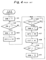
- the sector mark waiting signal SMW is generated by the sequencer 11 using the logic shown in Fig. 4.
- a SMW routine of Fig. 4 is initiated by turning ON the magnetic disk controller 1.
- Steps 401 through 404 carry out an initialization. That is, at step 401, the sector mark waiting signal SMW is made active ("1"), and at step 402, the sequencer 11 waits for a first sector mark detecting signal SMD which is, in this case, a first ID data read control signal IRD due to the activation of the sector mark waiting signal SMW. Once the first ID data read control signal IRD is made active, the control proceeds to step 403 which makes the sector mark waiting signal SMW inactive.
- a sector interval value N0 is read out of the RAM in dependence with the currently accessed zone and is set in a counter CNT0.
- the counter CNT0 is initialized to be counted down by a time interrupt routine as illustrated in Fig. 5 which is carried out at predetermined time intervals.
- the sector interval value N0 corresponds to a sector interval T0 as shown in Fig. 6A.
- a sector interval value N0 is read out of the RAM in dependence with the currently accessed zone and is set in the counter CNT0.
- a sector mark waiting signal width value N1 is read out of the RAM in dependence with the currently accessed zone and is set in a counter CNT1.
- both the counters CNT0 and CNT1 are initialized to be counted down by the routine as illustrated in Fig. 5.
- the sector mark waiting signal width value N1 corresponds to a sector mark waiting signal width T1 as shown in Fig. 6B.
- steps 405 through 410 are repeated, thus, the sector mark waiting signal SMW as shown in Fig. 6C is repeatedly set and reset.
- Fig. 5 note that the counter CNT0 is decremented by 1 at step 501, and the value of the counter CNT0 is guarded by 0 at steps 502 and 503. Similarly, the counter CNT1 is decremented by 1 at step 504, and the value of the counter CNT1 is guarded by 0 at steps 505 and 506. The routine of Fig. 5 is completed by step 507.
- the sequencer 11 reads ID data including a head number, a cylinder number which is, in this case, formed by a zone number and a track number, and a sector number on the data DA from the magnetic disk interface 3, and at step 702, it is determined whether or not a desired sector such as the fifth sector of the track 131 in the zone 121 is accessed. As a result, only when the desired sector is accessed, does the control proceed to step 703 which performs a write operation of sector data in the fifth sector of the track 131 in the zone 121 of the magnetic disk 110. Otherwise, the control proceeds to step 704. This routine is completed by step 704.
- the data from the location F to the location G of the track 132 is erased by an erroneous write operation.
- a magnetic disk controller 1' further includes an inverter 13, an AND circuit 14, and a RS flip-flop 15, in addition to the elements of the magnetic disk controller 1 of Fig. 3. Also, the CPU 2 generates a reset signal RST and transmits it to the sequencer 11 and the reset input of RS flip-flop 15. Thus, the RS flip-flop 15 is reset as occasion demands.
- the magnetic disk controller 1' of Fig. 8 When no deviation of the location of the magnetic head 4 occurs, the magnetic disk controller 1' of Fig. 8 operates in the same way as the magnetic disk controller 1 of Fig. 3. On the other hand, when a deviation of the location of the magnetic head 4 occurs, the magnetic disk controller 1' is operated so as to reduce the amount of data erased by an erroneous write operation.
- the magnetic disk controller 1' of Fig. 8 since the write operation is stopped just after an erroneous write operation is performed upon the location F to the location D of the sixth sector of the track 132, the data from the location D to the location G of the sixth sector of the track 132 is not erased. In other words, the seventh sector of the track 132 is not destroyed, and the erasure of data by an erroneous write operation due to the deviation of the location of the magnetic head 2 occurs in at most one sector.
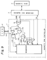
- a magnetic disk controller 1'' includes OR circuits 17 and 18 and AND circuits 19 and 20 in addition to the elements of the magnetic disk controller 1' of Fig. 8.
- the OR circuit 17 receives the sector mark waiting signal SMW and an index waiting signal IXW from a sequencer 11'' to generate a waiting signal W.
- the waiting signal W serves as the sector mark waiting signal SMW of Fig. 8.
- the OR circuit 18 receives the sector mark detecting signal SMD and an index detecting signal IXD from the disk interface unit 3, to generate a detecting signal D.
- the detecting signal D serves as the sector mark detecting signal SMD of Fig. 8.
- the index detecting signal IXD is generated at one revolution of the magnetic disk by using an optical sensor or a magnetic sensor (not shown).
- the AND circuit 19 passes the sector mark detecting signal SMD when the sector mark waiting signal SMW is active ("1"). In this case, the passed sector mark detecting signal SMD is denoted by SMWD.
- the AND circuit 20 passes the index detecting signal IXD when the index waiting signal IX is active ("1"). In this case, the passed index detecting signal IXD is denoted by IXWD.
- the sector mark waiting signal SMW of Fig. 9 is generated by a sequencer 11'' using the logic shown in Fig. 10 which is similar to that of Fig. 4. That is, in Fig. 10, step 402' is provided instead of step 402 of Fig. 4. That is, in Fig. 8, the ID data read control signal IRD is derived from the sector mark detecting signal SMD and the index detecting signal IXD, and it is impossible by the ID data read control signal IRD to discriminate the sector detecting signal SMD from the index detecting signal IXD. Therefore, in this case, an initialization for the first sector mark detecting signal SMD is carried out by using the signal SMWD through the AND circuit 19.
- the index waiting signal IXW is generated by the sequencer 11'' using the logic shown in Fig. 11, which is similar to Fig. 10. That is, an IXW routine of Fig. 11 is initiated by turning ON the magnetic disk controller 1''. Steps 1101 through 1104 carry out an initialization. That is, at step 1101, the index waiting signal IXW is made active ("1"), and at step 1102, the sequencer 11 waits for a first sector mark detecting signal IXD which is, in this case, a first signal IXWD due to the activation of the index waiting signal IXW. Once the first IXWD is made active, the control proceeds to step 1103 which makes the index waiting signal IXW inactive.
- an index interval value N2 is set in a counter CNT2.
- the counter CNT2 is initialized to be counted down by a time interrupt routine as illustrated in Fig. 12 which is carried out at predetermined time intervals.
- the index interval value N2 corresponds to an index interval T2 as shown in Fig. 13A.
- an index interval value N2 is set in the counter CNT2.
- an index waiting signal width value N3 is set in a counter CNT3.
- both the counters CNT2 and CNT3 are initialized to be counted down by the routine as illustrated in Fig. 12.
- the index waiting signal width value N3 corresponds to an index waiting signal width T3 as shown in Fig. 13B.
- steps 1105 through 1110 are repeated, and thus, the index waiting signal IXW as shown in Fig. 13C is repeatedly set and reset.
- steps 1201 through 1206 are added to the routine of Fig. 5. That is, the counter CNT2 is decremented by 1 at step 1201, and the value of the counter CNT2 is guarded by 0 at steps 1202 and 1203. Similarly, the counter CNT3 is decremented by 1 at step 1204, and the value of the counter CNT3 is guarded by 0 at steps 1205 and 1206.
- the routine of Fig. 12 is completed by step 507.
- the present invention when a deviation of the location of the magnetic head occurs due to the vibration of the magnetic disk unit or the like, the amount of erased or destroyed data can be reduced.
Landscapes
- Signal Processing For Digital Recording And Reproducing (AREA)
- Moving Of The Head To Find And Align With The Track (AREA)
Applications Claiming Priority (2)
| Application Number | Priority Date | Filing Date | Title |
|---|---|---|---|
| JP4288044A JPH06139732A (ja) | 1992-10-27 | 1992-10-27 | 磁気ディスクコントローラ |
| JP288044/92 | 1992-10-27 |
Publications (3)
| Publication Number | Publication Date |
|---|---|
| EP0595249A2 true EP0595249A2 (de) | 1994-05-04 |
| EP0595249A3 EP0595249A3 (en) | 1995-12-06 |
| EP0595249B1 EP0595249B1 (de) | 1998-09-16 |
Family
ID=17725112
Family Applications (1)
| Application Number | Title | Priority Date | Filing Date |
|---|---|---|---|
| EP93117302A Expired - Lifetime EP0595249B1 (de) | 1992-10-27 | 1993-10-26 | Magnetdisksteuereinrichtung, die fähig ist, fehlerhafte Schreiboperation zu vermeiden |
Country Status (5)
| Country | Link |
|---|---|
| US (2) | US5559647A (de) |
| EP (1) | EP0595249B1 (de) |
| JP (1) | JPH06139732A (de) |
| KR (1) | KR0138967B1 (de) |
| DE (1) | DE69321067T2 (de) |
Cited By (2)
| Publication number | Priority date | Publication date | Assignee | Title |
|---|---|---|---|---|
| US5559647A (en) * | 1992-10-27 | 1996-09-24 | Nec Corporation | Magnetic disk controller which avoids erroneous write operations to ZBR-type magnetic disks upon detection of a next sector mark from the ZBR magnetic disk |
| CN1071475C (zh) * | 1995-04-28 | 2001-09-19 | 索尼公司 | 数字信号处理器 |
Families Citing this family (5)
| Publication number | Priority date | Publication date | Assignee | Title |
|---|---|---|---|---|
| JP2635939B2 (ja) * | 1994-09-29 | 1997-07-30 | インターナショナル・ビジネス・マシーンズ・コーポレイション | 情報記録媒体、ヘッド位置識別情報の生成方法、ヘッド位置判定方法、及び情報記録・読取装置 |
| KR0176615B1 (ko) * | 1996-07-27 | 1999-04-15 | 삼성전자주식회사 | 하드 디스크 드라이브 제어장치 및 그 방법 |
| US5802118A (en) * | 1996-07-29 | 1998-09-01 | Cirrus Logic, Inc. | Sub-sampled discrete time read channel for computer storage systems |
| US6167461A (en) * | 1998-03-31 | 2000-12-26 | Texas Instruments Incorporated | Programmable high performance disk formatter for headerless disk drive controller executing a series of low level instructions generated by a high level processing engine |
| US6583945B1 (en) | 1998-10-30 | 2003-06-24 | Iomega Corporation | Method for irreversibly write-securing a magnetic storage cartridge |
Family Cites Families (22)
| Publication number | Priority date | Publication date | Assignee | Title |
|---|---|---|---|---|
| US3819281A (en) * | 1971-12-27 | 1974-06-25 | Sperry Rand Corp | Index-sector detection scheme for magnetic disc memory |
| US3864755A (en) * | 1973-08-20 | 1975-02-04 | Memorex Corp | Thermoformed cartridge for a magnetic record disc |
| US3864735A (en) * | 1973-09-12 | 1975-02-04 | Burroughs Corp | Read/write system for high density magnetic recording |
| US4583208A (en) * | 1984-02-08 | 1986-04-15 | Optical Storage International-U.S. | Sector mark decoder for an optical recorder |
| JPH0760574B2 (ja) * | 1984-03-26 | 1995-06-28 | 株式会社日立製作所 | 光デイスク装置のセクタ開始信号発生回路 |
| JP2581663B2 (ja) * | 1985-05-02 | 1997-02-12 | 株式会社日立製作所 | 光ディスク |
| US4823212A (en) * | 1986-11-26 | 1989-04-18 | Hewlett-Packard Company | Sampled servo code format and system for a disc drive |
| US4979056A (en) * | 1987-06-02 | 1990-12-18 | Conner Peripherals, Inc. | Disk drive system controller architecture |
| US4979055A (en) * | 1987-06-02 | 1990-12-18 | Conner Peripherals, Inc. | Disk drive system controller architecture utilizing embedded real-time diagnostic monitor |
| JP2550588B2 (ja) * | 1987-07-16 | 1996-11-06 | 日本電気株式会社 | ディスク装置 |
| US5083303A (en) * | 1988-04-28 | 1992-01-21 | Olympus Optical Co., Ltd. | Sector mark detecting apparatus in optical disc apparatus |
| JPH01285064A (ja) * | 1988-05-11 | 1989-11-16 | Canon Inc | 情報ディスクドライブ装置 |
| JP2819294B2 (ja) * | 1988-09-29 | 1998-10-30 | キヤノン株式会社 | デジタル情報再生装置 |
| US5343453A (en) * | 1988-12-01 | 1994-08-30 | Canon Kabushiki Kaisha | Method for accessing desired track on disk with plurality of recording zones with head, and apparatus therefore |
| JPH0444688A (ja) * | 1990-06-12 | 1992-02-14 | Ricoh Co Ltd | 光ディスク駆動装置 |
| US5278712A (en) * | 1990-07-19 | 1994-01-11 | Kabushiki Kaisha Toshiba | Removable disk drive having two heads formed with a gimbal structure |
| JP2846441B2 (ja) * | 1990-09-26 | 1999-01-13 | ティアック株式会社 | 光ディスク再生装置 |
| JP2596222B2 (ja) * | 1990-12-18 | 1997-04-02 | 松下電器産業株式会社 | 磁気ディスク及び磁気ディスク装置 |
| US5257143A (en) * | 1991-01-15 | 1993-10-26 | Zenith Data Systems Corporation | Method and apparatus for positioning head of disk drive using zone-bit-recording |
| US5321560A (en) * | 1991-09-25 | 1994-06-14 | Integral Peripherals, Inc. | Embedded servo system for low power disk drives |
| KR100261196B1 (ko) * | 1991-12-02 | 2000-07-01 | 이데이 노부유끼 | 자기 디스크 기록매체의 어드레스 정보 검출장치 |
| JPH06139732A (ja) * | 1992-10-27 | 1994-05-20 | Nec Ic Microcomput Syst Ltd | 磁気ディスクコントローラ |
-
1992
- 1992-10-27 JP JP4288044A patent/JPH06139732A/ja active Pending
-
1993
- 1993-10-26 EP EP93117302A patent/EP0595249B1/de not_active Expired - Lifetime
- 1993-10-26 DE DE69321067T patent/DE69321067T2/de not_active Expired - Fee Related
- 1993-10-26 KR KR1019930022286A patent/KR0138967B1/ko not_active Expired - Fee Related
-
1995
- 1995-03-08 US US08/400,571 patent/US5559647A/en not_active Expired - Fee Related
- 1995-10-24 US US08/547,409 patent/US5654835A/en not_active Expired - Fee Related
Cited By (3)
| Publication number | Priority date | Publication date | Assignee | Title |
|---|---|---|---|---|
| US5559647A (en) * | 1992-10-27 | 1996-09-24 | Nec Corporation | Magnetic disk controller which avoids erroneous write operations to ZBR-type magnetic disks upon detection of a next sector mark from the ZBR magnetic disk |
| US5654835A (en) * | 1992-10-27 | 1997-08-05 | Nec Corporation | Magnetic disk controller capable of avoiding erroneous write operations to ZBR-type magnetic disks |
| CN1071475C (zh) * | 1995-04-28 | 2001-09-19 | 索尼公司 | 数字信号处理器 |
Also Published As
| Publication number | Publication date |
|---|---|
| JPH06139732A (ja) | 1994-05-20 |
| DE69321067D1 (de) | 1998-10-22 |
| DE69321067T2 (de) | 1999-05-27 |
| EP0595249B1 (de) | 1998-09-16 |
| US5559647A (en) | 1996-09-24 |
| EP0595249A3 (en) | 1995-12-06 |
| KR0138967B1 (ko) | 1998-06-01 |
| KR940010031A (ko) | 1994-05-24 |
| US5654835A (en) | 1997-08-05 |
Similar Documents
| Publication | Publication Date | Title |
|---|---|---|
| US3997876A (en) | Apparatus and method for avoiding defects in the recording medium within a peripheral storage system | |
| US4541019A (en) | Recording system for recording data on tape in a disk-recording format | |
| JP2798327B2 (ja) | データ処理装置を制御する方法 | |
| US5317468A (en) | Magnetic disk having reserve servo sectors and plural reserve tracks | |
| US6154330A (en) | Disk provided with servo patterns and method of recording servo patterns | |
| EP0595249B1 (de) | Magnetdisksteuereinrichtung, die fähig ist, fehlerhafte Schreiboperation zu vermeiden | |
| US4754344A (en) | Method and apparatus for formatting magnetic disks with use of host equipment programmed for smaller capacity magnetic disks | |
| US3686650A (en) | Addressing system with means to check mechanical stability | |
| EP0459726A2 (de) | Magnetplattengerät | |
| KR100273820B1 (ko) | 자기기록 매체 및 그 자기기록 재생장치 | |
| JP2003109293A (ja) | ディスク装置を含むシステムにおける環境仕様違反時処理方法及びシステム | |
| KR920001156B1 (ko) | 컴퓨터용 자기헤드 | |
| US7167332B2 (en) | Method and apparatus for recording data onto a recording medium including warning of the approach to an end of medium position | |
| JP3196112B2 (ja) | カード型記憶媒体の複製方法 | |
| US7848049B2 (en) | Magnetic disk apparatus and magnetic disk access control method | |
| US4791500A (en) | Method and apparatus for writing information on magnetic disk with single-gap magnetic head | |
| JPS63193388A (ja) | デイスクドライブシステム | |
| JPS58169376A (ja) | 磁気デイスクのサ−ボデ−タ記録方式 | |
| JPH02198051A (ja) | 磁気テープ装置 | |
| JPS63193394A (ja) | 光学式記録媒体におけるデ−タ管理方式 | |
| JPS62229575A (ja) | 磁気デイスク装置 | |
| JPH01128275A (ja) | 情報記録装置のオン/オフトラック表示装置 | |
| JPS6242353A (ja) | トラツク識別方法 | |
| JPH0192928A (ja) | 光磁気情報記録及び消去装置 | |
| JPS6117056B2 (de) |
Legal Events
| Date | Code | Title | Description |
|---|---|---|---|
| PUAI | Public reference made under article 153(3) epc to a published international application that has entered the european phase |
Free format text: ORIGINAL CODE: 0009012 |
|
| AK | Designated contracting states |
Kind code of ref document: A2 Designated state(s): DE FR GB NL |
|
| PUAL | Search report despatched |
Free format text: ORIGINAL CODE: 0009013 |
|
| AK | Designated contracting states |
Kind code of ref document: A3 Designated state(s): DE FR GB NL |
|
| 17P | Request for examination filed |
Effective date: 19960311 |
|
| 17Q | First examination report despatched |
Effective date: 19970224 |
|
| GRAG | Despatch of communication of intention to grant |
Free format text: ORIGINAL CODE: EPIDOS AGRA |
|
| GRAG | Despatch of communication of intention to grant |
Free format text: ORIGINAL CODE: EPIDOS AGRA |
|
| GRAH | Despatch of communication of intention to grant a patent |
Free format text: ORIGINAL CODE: EPIDOS IGRA |
|
| GRAH | Despatch of communication of intention to grant a patent |
Free format text: ORIGINAL CODE: EPIDOS IGRA |
|
| GRAA | (expected) grant |
Free format text: ORIGINAL CODE: 0009210 |
|
| AK | Designated contracting states |
Kind code of ref document: B1 Designated state(s): DE FR GB NL |
|
| REF | Corresponds to: |
Ref document number: 69321067 Country of ref document: DE Date of ref document: 19981022 |
|
| ET | Fr: translation filed | ||
| PLBE | No opposition filed within time limit |
Free format text: ORIGINAL CODE: 0009261 |
|
| STAA | Information on the status of an ep patent application or granted ep patent |
Free format text: STATUS: NO OPPOSITION FILED WITHIN TIME LIMIT |
|
| 26N | No opposition filed | ||
| PGFP | Annual fee paid to national office [announced via postgrant information from national office to epo] |
Ref country code: FR Payment date: 20001010 Year of fee payment: 8 |
|
| PGFP | Annual fee paid to national office [announced via postgrant information from national office to epo] |
Ref country code: DE Payment date: 20001016 Year of fee payment: 8 |
|
| PGFP | Annual fee paid to national office [announced via postgrant information from national office to epo] |
Ref country code: GB Payment date: 20001025 Year of fee payment: 8 |
|
| PGFP | Annual fee paid to national office [announced via postgrant information from national office to epo] |
Ref country code: NL Payment date: 20001026 Year of fee payment: 8 |
|
| PG25 | Lapsed in a contracting state [announced via postgrant information from national office to epo] |
Ref country code: GB Free format text: LAPSE BECAUSE OF NON-PAYMENT OF DUE FEES Effective date: 20011026 |
|
| REG | Reference to a national code |
Ref country code: GB Ref legal event code: IF02 |
|
| PG25 | Lapsed in a contracting state [announced via postgrant information from national office to epo] |
Ref country code: NL Free format text: LAPSE BECAUSE OF NON-PAYMENT OF DUE FEES Effective date: 20020501 |
|
| GBPC | Gb: european patent ceased through non-payment of renewal fee |
Effective date: 20011026 |
|
| PG25 | Lapsed in a contracting state [announced via postgrant information from national office to epo] |
Ref country code: FR Free format text: LAPSE BECAUSE OF NON-PAYMENT OF DUE FEES Effective date: 20020628 |
|
| NLV4 | Nl: lapsed or anulled due to non-payment of the annual fee |
Effective date: 20020501 |
|
| PG25 | Lapsed in a contracting state [announced via postgrant information from national office to epo] |
Ref country code: DE Free format text: LAPSE BECAUSE OF NON-PAYMENT OF DUE FEES Effective date: 20020702 |
|
| REG | Reference to a national code |
Ref country code: FR Ref legal event code: ST |