EP0595537B1 - Überwachung der optischer Verstärkung eines optischen Halbleiterverstärkers - Google Patents
Überwachung der optischer Verstärkung eines optischen Halbleiterverstärkers Download PDFInfo
- Publication number
- EP0595537B1 EP0595537B1 EP93308336A EP93308336A EP0595537B1 EP 0595537 B1 EP0595537 B1 EP 0595537B1 EP 93308336 A EP93308336 A EP 93308336A EP 93308336 A EP93308336 A EP 93308336A EP 0595537 B1 EP0595537 B1 EP 0595537B1
- Authority
- EP
- European Patent Office
- Prior art keywords
- section
- input
- output
- optical amplifier
- sections
- Prior art date
- Legal status (The legal status is an assumption and is not a legal conclusion. Google has not performed a legal analysis and makes no representation as to the accuracy of the status listed.)
- Expired - Lifetime
Links
Images

Classifications
-
- H—ELECTRICITY
- H01—ELECTRIC ELEMENTS
- H01S—DEVICES USING THE PROCESS OF LIGHT AMPLIFICATION BY STIMULATED EMISSION OF RADIATION [LASER] TO AMPLIFY OR GENERATE LIGHT; DEVICES USING STIMULATED EMISSION OF ELECTROMAGNETIC RADIATION IN WAVE RANGES OTHER THAN OPTICAL
- H01S5/00—Semiconductor lasers
- H01S5/50—Amplifier structures not provided for in groups H01S5/02 - H01S5/30
-
- H—ELECTRICITY
- H01—ELECTRIC ELEMENTS
- H01S—DEVICES USING THE PROCESS OF LIGHT AMPLIFICATION BY STIMULATED EMISSION OF RADIATION [LASER] TO AMPLIFY OR GENERATE LIGHT; DEVICES USING STIMULATED EMISSION OF ELECTROMAGNETIC RADIATION IN WAVE RANGES OTHER THAN OPTICAL
- H01S5/00—Semiconductor lasers
- H01S5/06—Arrangements for controlling the laser output parameters, e.g. by operating on the active medium
- H01S5/062—Arrangements for controlling the laser output parameters, e.g. by operating on the active medium by varying the potential of the electrodes
- H01S5/0625—Arrangements for controlling the laser output parameters, e.g. by operating on the active medium by varying the potential of the electrodes in multi-section lasers
Definitions
- This invention relates generally to semiconductor devices and, more particularly, to a semiconductor device which provides optical gain monitoring when operated as an optical amplifier.
- Semiconductor laser amplifiers are becoming increasingly more important components for optical signal processing applications. In addition to simple loss compensation and switching functions, a semiconductor laser amplifier can provide simultaneous amplification and detection of an optical signal. Recently, amplifiers which exploit this dual capability have demonstrated improved detection capability by employing a split contact and performing the detecting function at the rear contact. See C. Jorgensen et al., "Two-Section Semiconductor Optical Amplifier Used as an Efficient Channel Dropping Node", IEEE Photon. Technol. Letters, Vol. 4, pp. 348-350, 1992.
- EP-A-0 377 948 discloses a semiconductor optical amplifier comprising an input section, an output section and a middle section including a gain medium and a continuous optical waveguide which extend through said input, middle and output sections.
- This invention is directed toward satisfying this need of monitoring the optical gain of a semiconductor laser amplifier.
- the invention is defined in claim 1 and relates to a semiconductor laser amplifier which, in addition to amplifying an optical signal, can also be used for monitoring the amplifier gain. It has been discovered that when a semiconductor laser amplifier is electrically, not optically, split into three separate sections, two end sections and a middle section, and the three sections are forward biased in parallel, the optical gain of the semiconductor amplifier is related to the ratio of the voltages at the two end sections; and this relationship depends only on fixed quantities such as the lengths of the three sections.
- FIG. 1 schematically illustrates structure according to the invention for monitoring the optical gain of a semiconductor laser amplifier.
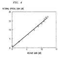
- FIG. 4 is a graphical representation of amplifier internal optical gain vs. voltage gain of the semiconductor laser amplifier.
- the gain of a semiconductor optical amplifier can be monitored by splitting the semiconductor optical amplifier into three electrically isolated sections which extend along a continuous optical waveguide.
- a first section is located at the input end of the amplifier, a second section is located at the output end of the amplifier, and a middle section is located between the first and second sections.
- Each section supports an electrical contact which is used to individually forward bias each section.
- the ratio of the voltages at the contacts coupled to the first or input section and third or output section is related to the gain of the amplifier.
- FIG. 1 there is illustrated a schematic diagram of a semiconductor laser amplifier which provides monitoring of the optical gain.
- the semiconductor amplifier 10 material can be grown using atmospheric pressure metalorganic vapor phase epitaxy.
- the base wafer comprises a strain-compensated 1.55 ⁇ m wavelength multiquantum well gain layer 11 on top of a 280nm (2800 ⁇ ) thick InGaAsP passive waveguide 13 similar to that in B. I. Miller et al., "Strain-Compensated Strained-Layer Superlattices for 1.5 ⁇ m Wavelength Lasers", Appl. Phys. Lett., vol. 58, pp. 1952-1954, 1991.
- the quantum well stack is composed of six 3nm (30 ⁇ ) thick InGaAs wells with 1.3% compressive strain separated by 12.5nm (125 ⁇ ) thick InGaAsP barriers with 0.2% tensile strain having peak photoluminescence wavelength of 1.25 ⁇ m.
- the semiconductor amplifier 10 uses the semi-insulating planar buried-heterostructure as disclosed by U. Koren et al., "Semi-Insulating Blocked Planar Buried Heterostructure GaInAs-InP Laser With High Power and High Modulation Bandwidth", Electron. Lett., vol. 24, pp. 138-139, 1988.
- the semiconductor amplifier 10 is 880 ⁇ m long with the top contact divided into three sections; a 640 ⁇ m middle section 12 and 100 ⁇ m input and output sections 14, 16 at the front and rear facets separated by 20 ⁇ m gaps 18, 20.
- the three sections 12, 14 and 16 are electrically isolated from each other by implanting ions in the gap regions 18, 20. Ions which can be used for this purpose can include, but are not limited to hydrogen, helium and fluorine. With the three sections forward biased, the device was found to have a lasing threshold of 30 mA before the facets are anti-reflection coated.
- n and p are small-signal carrier density and photon density modulation amplitudes
- g n and g are differential gain and unsaturated material gain
- P o is steady-state photon density
- v g is group velocity
- ⁇ sp carrier spontaneous lifetime
- the internal Gain G of the amplifier is the ratio of the input and output photon density modulation.
- FIG. 1 there is illustrated a semiconductor amplifier embodying the invention connected to enable its optical gain to be monitored.
- an optical input signal P in from an MQW distributed Bragg reflector laser at 1.561 ⁇ m is directly modulated by a 50 MHz sine wave.
- the light is then attenuated and coupled into the amplifier 10 with an objective lens.
- the input light is TE polarized and, in this instance, the average incident optical power is determined to be -6 dBm.
- the three sections 14, 12, 16 of the semiconductor amplifier 10 are forward biased in parallel; and the ac voltage signals at the contacts of sections 14, 16 are coupled out with a pair of bias tees made up of condensers 22, 24 and inductors 26, 28.
- the ac signal from the contact on top of section 14 is electrically amplified by amplifier 30; and the ac signal from the contact on top of section 16 is electrically amplified by amplifier 32.
- the gain of the semiconductor amplifier is proportional to the ratio of the amplified signals from amplifiers 30, 32.
- the amplified optical signal P out from the semiconductor amplifier 10 is collected with a second objective lens and monitored with an optical power meter, where the detected power from background spontaneous emission is subtracted from the measurement.
- the voltage signals from the contacts on sections 14, 16 are then correlated with the amplifier optical gain.
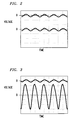
- FIGs. 2 and 3 illustrate typical test results.
- the voltages are measured as a function of amplifier bias current I dc for constant average incident optical power.
- I dc 26mA of bias
- the semiconductor amplifier 10 operated near zero loss where the voltage gain is unity.
- the top plot is the voltage at the input section 14 and the bottom plot in the voltage at the output section 16.
- the voltage gain is 12.1 dB.
- the top plot is the voltage at the input section 14 and the bottom plot is the voltage at the output section 16, shown at half scale.
- FIG. 4 illustrates the internal gain of the semiconductor amplifier 10 vs. voltage gain for the same range of bias currents.
- the optical signal gain at 110 mA of bias is 7.2 dB, and the input coupling loss and ⁇ gap are estimated to be -9 dB and 60cm -1 respectively to give 16.2 dB internal gain at the bias current.
- the slope of the line which is independent of estimates for coupling and ⁇ gap , is 1.35, which is slightly higher than the theoretical value of 1.14.
- a more detailed theoretical treatment which includes gain saturation effects could possibly account for the small discrepancy.
Landscapes
- Physics & Mathematics (AREA)
- Condensed Matter Physics & Semiconductors (AREA)
- General Physics & Mathematics (AREA)
- Electromagnetism (AREA)
- Optics & Photonics (AREA)
- Semiconductor Lasers (AREA)
- Lasers (AREA)
Claims (12)
- Optischer Halbleiterverstärker miteinem Eingangsabschnitt (14), einem Ausgangsabschnitt (16) und einem zwischen dem Eingangsabschnitt und dem Ausgangsabschnitt angeordneten Mittelabschnitt (12) und mit einem Verstärkungsmedium (11) und einem durchgehenden optischen Wellenleiter, der sich durch den Eingangsabschnitt, den Mittelabschnitt und den Ausgangsabschnitt hindurcherstreckt, dadurch gekennzeichnet, daß er auchMittel (18, 20) zum elektrischen Trennen von Eingangsabschnitt, Mittelabschnitt und Ausgangsabschnitt voneinander,angekoppelte Mittel (Idc), um an jeden der drei Abschnitte eine Durchlaßvorspannung anzulegen, undangekoppelte Mittel (22, 24, 26, 28, 30, 32) zum Erfassen der Spannungsänderung am Eingangsabschnitt und am Ausgangsabschnitt, so daß die optische Verstärkung des Verstärkers durch Vergleichen der Spannungsänderungen an dem Eingangsabschnitt und dem Ausgangsabschnitt überwacht werden kann, enthält.
- Optischer Halbleiterverstärker nach Anspruch 1, weiterhin mit
angekoppelten Mitteln, um das Verhältnis aus der Spannung am Eingangsabschnitt und am Ausgangsabschnitt zu bestimmen. - Optischer Halbleiterverstärker nach Anspruch 1 miteinem an den Eingangsabschnitt angekoppelten ersten elektrischen Kontakt (14) zum Anlegen einer Durchlaßvorspannung an den Eingangsabschnitt,einem an den Mittelabschnitt angekoppelten zweiten elektrischen Kontakt (12) zum Anlegen einer Durchlaßvorspannung an den Mittelabschnitt undeinem an den Ausgangsabschnitt angekoppelten dritten elektrischen Kontakt (16) zum Anlegen einer Durchlaßvorspannung an den Ausgangsabschnitt.
- Optischer Halbleiterverstärker nach Anspruch 3, wobei
der Eingangsabschnitt und der Ausgangsabschnitt jeweils eine Länge aufweisen, die unter der Länge des Mittelabschnitts liegt. - Optischer Halbleiterverstärker nach Anspruch 3 oder 4, wobei
der Eingangsabschnitt, der Ausgangsabschnitt und der Mittelabschnitt jeweils eine Länge aufweisen, die im wesentlichen gleich ist. - Optischer Halbleiterverstärker nach einem der vorhergehenden Ansprüche, wobei
jeder elektrische Kontakt im wesentlichen die ganze Oberfläche seines zugeordneten Abschnitts überdeckt und jeder elektrische Kontakt von jedem anderen elektrisch getrennt ist. - Optischer Halbleiterverstärker nach einem der vorhergehenden Ansprüche, wobei
das Mittel zum elektrischen Trennen des Eingangsabschnitts, des Ausgangsabschnitts und des Mittelabschnitts voneinander Ionen umfaßt, die in dem zwischen dem Eingangsabschnitt und dem Mittelabschnitt und dem Mittelabschnitt und dem Ausgangsabschnitt liegenden Bereich in das Halbleiterbauelement implantiert worden sind. - Optischer Halbleiterverstärker nach Anspruch 7, wobei es sich bei den im Halbleiterbauelement implantierten Ionen um Wasserstoffionen handelt.
- Optischer Halbleiterverstärker nach Anspruch 7, wobei es sich bei den im Halbleiterbauelement implantierten Ionen um Heliumionen handelt.
- Optischer Halbleiterverstärker nach Anspruch 7, wobei es sich bei den im Halbleiterbauelement implantierten Ionen um Fluorionen handelt.
- Optischer Halbleiterverstärker nach einem der vorhergehenden Ansprüche, wobeijeweils am Eingangsabschnitt, am Mittelabschnitt und am Ausgangsabschnitt Durchlaßvorspannung anliegt,erste Mittel (22, 26, 30) an den Eingangsabschnitt angekoppelt sind, um das Vorspannungspotential am Eingangsabschnitt zu erfassen, undzweite Mittel (24, 28, 32) an den Ausgangsabschnitt angekoppelt sind, um das Vorspannungspotential am Ausgangsabschnitt zu erfassen.
- Optischer Halbleiterverstärker nach Anspruch 11, wobeider Eingangsabschnitt über einen ersten Vorspannungsabzweig (22, 26) an das Vorspannungsmittel angekoppelt ist;der Ausgangsabschnitt über einen zweiten Vorspannungsabzweig (28, 24) an das Vorspannungsmittel angekoppelt ist; undder Mittelabschnitt direkt an das Vorspannungsmittel angekoppelt ist.
Applications Claiming Priority (2)
| Application Number | Priority Date | Filing Date | Title |
|---|---|---|---|
| US967593 | 1992-10-28 | ||
| US07/967,593 US5309469A (en) | 1992-10-28 | 1992-10-28 | Monitoring optical gain of semiconductor optical amplifier |
Publications (2)
| Publication Number | Publication Date |
|---|---|
| EP0595537A1 EP0595537A1 (de) | 1994-05-04 |
| EP0595537B1 true EP0595537B1 (de) | 1997-03-19 |
Family
ID=25513020
Family Applications (1)
| Application Number | Title | Priority Date | Filing Date |
|---|---|---|---|
| EP93308336A Expired - Lifetime EP0595537B1 (de) | 1992-10-28 | 1993-10-20 | Überwachung der optischer Verstärkung eines optischen Halbleiterverstärkers |
Country Status (4)
| Country | Link |
|---|---|
| US (1) | US5309469A (de) |
| EP (1) | EP0595537B1 (de) |
| JP (1) | JP2735474B2 (de) |
| DE (1) | DE69308984T2 (de) |
Families Citing this family (6)
| Publication number | Priority date | Publication date | Assignee | Title |
|---|---|---|---|---|
| US5371757A (en) * | 1993-10-22 | 1994-12-06 | The United States Of America As Represented By The Secretary Of The Air Force | Integrated semiconductor laser oscillator and off-axis amplifier |
| EP1130718A3 (de) * | 2000-01-20 | 2003-07-02 | Cyoptics (Israel) Ltd. | Stabilisierter frequenzverstimmbarer Laser mit Fasergitter |
| US6760350B1 (en) * | 2002-04-12 | 2004-07-06 | The United States Of America As Represented By The National Security Agency | Method for measuring gain of photonic inverters |
| US6771682B2 (en) * | 2002-08-12 | 2004-08-03 | Infinera Corporation | Electrical isolation of optical components in photonic integrated circuits (PICs) |
| KR100617693B1 (ko) * | 2003-08-20 | 2006-08-28 | 삼성전자주식회사 | 광검출기를 구비하는 반도체 광증폭 장치 및 그 제조방법 |
| JP2005135956A (ja) * | 2003-10-28 | 2005-05-26 | Mitsubishi Electric Corp | 半導体光増幅器およびその製造方法ならびに光通信デバイス |
Family Cites Families (5)
| Publication number | Priority date | Publication date | Assignee | Title |
|---|---|---|---|---|
| US4523961A (en) * | 1982-11-12 | 1985-06-18 | At&T Bell Laboratories | Method of improving current confinement in semiconductor lasers by inert ion bombardment |
| JPS62291987A (ja) * | 1986-06-12 | 1987-12-18 | Mitsubishi Electric Corp | 光集積化素子 |
| JPH02184828A (ja) * | 1989-01-12 | 1990-07-19 | Toshiba Corp | 半導体光増幅器 |
| US5099489A (en) * | 1989-09-15 | 1992-03-24 | At&T Bell Laboratories | Apparatus comprising a quantum well device |
| EP0562518B1 (de) * | 1992-03-23 | 1997-12-29 | Canon Kabushiki Kaisha | Optische Vorrichtung und Methode unter Benutzung dieser Vorrichtung, welche die Änderung einer über die beiden Anschlussenden eines verstärkenden Bereichs abfallenden Spannung ausnutzt |
-
1992
- 1992-10-28 US US07/967,593 patent/US5309469A/en not_active Expired - Lifetime
-
1993
- 1993-10-20 DE DE69308984T patent/DE69308984T2/de not_active Expired - Lifetime
- 1993-10-20 EP EP93308336A patent/EP0595537B1/de not_active Expired - Lifetime
- 1993-10-26 JP JP5288772A patent/JP2735474B2/ja not_active Expired - Lifetime
Also Published As
| Publication number | Publication date |
|---|---|
| EP0595537A1 (de) | 1994-05-04 |
| JP2735474B2 (ja) | 1998-04-02 |
| DE69308984D1 (de) | 1997-04-24 |
| JPH06216434A (ja) | 1994-08-05 |
| DE69308984T2 (de) | 1997-07-03 |
| US5309469A (en) | 1994-05-03 |
Similar Documents
| Publication | Publication Date | Title |
|---|---|---|
| Newkirk et al. | 1.5 mu m multiquantum-well semiconductor optical amplifier with tensile and compressively strained wells for polarization-independent gain | |
| US20080291952A1 (en) | Optical semiconductor device | |
| EP0827243A1 (de) | Optische Halbleitervorrichtung und Herstellungsverfahren | |
| JP3238727B2 (ja) | 光増幅器 | |
| Magari et al. | Polarization-insensitive optical amplifier with tensile-strained-barrier MQW structure | |
| EP0456043A2 (de) | Monolithisch integrierter optischer Halbleitervorverstärker | |
| US8179592B2 (en) | Semiconductor optical amplifier, method for manufacturing the same, and semiconductor optical integrated device | |
| CA2014937C (en) | Laser-photodetector assemblage | |
| Wu et al. | InGaAsP/InP vertical directional coupler filter with optimally designed wavelength tunability | |
| EP0595537B1 (de) | Überwachung der optischer Verstärkung eines optischen Halbleiterverstärkers | |
| JPH08250821A (ja) | 半導体光ソース | |
| CA2014938C (en) | Optical amplifier-photodetector assemblage | |
| Kitamura et al. | Polarization-insensitive semiconductor optical amplifier array grown by selective MOVPE | |
| Sysak et al. | A single regrowth integration platform for photonic circuits incorporating tunable SGDBR lasers and quantum-well EAMs | |
| Buus et al. | A theoretical and experimental investigation of Fabry-Perot semiconductor laser amplifiers | |
| Shtengel et al. | Advances in measurements of physical parameters of semiconductor lasers | |
| Newkirk et al. | Three-section semiconductor optical amplifier for monitoring of optical gain | |
| EP0356189B1 (de) | Optischer Halbleiterverstärker mit verkürzter Gewinn-Erholungszeit | |
| EP1677395B1 (de) | Optische Verstärkungsvorrichtung | |
| Sakakibara et al. | Very narrow spectral linewidth of GaInAs MQW-DFB-PPIBH laser diodes | |
| Kjebon et al. | Two-section InGaAsP DBR-lasers at 1.55/spl mu/m wavelength with 31 GHz direct modulation bandwidth | |
| Doussiere et al. | New laser structure for polarization insensitive semiconductor amplifier with low current consumption | |
| Dutta et al. | Performance comparison of InGaAsP lasers emitting at 1.3 and 1.55 μm for lightwave system applications | |
| Chawki et al. | Two-electrode DFB laser filter used as a wide tunable narrow-band FM receiver: tuning analysis, characteristics and experimental FSK-WDM system | |
| JPH0774427A (ja) | 半導体レーザ素子とレーザモジュール |
Legal Events
| Date | Code | Title | Description |
|---|---|---|---|
| PUAI | Public reference made under article 153(3) epc to a published international application that has entered the european phase |
Free format text: ORIGINAL CODE: 0009012 |
|
| AK | Designated contracting states |
Kind code of ref document: A1 Designated state(s): DE FR GB NL |
|
| RAP3 | Party data changed (applicant data changed or rights of an application transferred) |
Owner name: AT&T CORP. |
|
| 17P | Request for examination filed |
Effective date: 19941021 |
|
| GRAG | Despatch of communication of intention to grant |
Free format text: ORIGINAL CODE: EPIDOS AGRA |
|
| GRAH | Despatch of communication of intention to grant a patent |
Free format text: ORIGINAL CODE: EPIDOS IGRA |
|
| 17Q | First examination report despatched |
Effective date: 19960802 |
|
| GRAH | Despatch of communication of intention to grant a patent |
Free format text: ORIGINAL CODE: EPIDOS IGRA |
|
| GRAA | (expected) grant |
Free format text: ORIGINAL CODE: 0009210 |
|
| AK | Designated contracting states |
Kind code of ref document: B1 Designated state(s): DE FR GB NL |
|
| ET | Fr: translation filed | ||
| REF | Corresponds to: |
Ref document number: 69308984 Country of ref document: DE Date of ref document: 19970424 |
|
| PLBE | No opposition filed within time limit |
Free format text: ORIGINAL CODE: 0009261 |
|
| 26N | No opposition filed | ||
| PGFP | Annual fee paid to national office [announced via postgrant information from national office to epo] |
Ref country code: NL Payment date: 20000925 Year of fee payment: 8 |
|
| PGFP | Annual fee paid to national office [announced via postgrant information from national office to epo] |
Ref country code: FR Payment date: 20010925 Year of fee payment: 9 |
|
| REG | Reference to a national code |
Ref country code: GB Ref legal event code: IF02 |
|
| PG25 | Lapsed in a contracting state [announced via postgrant information from national office to epo] |
Ref country code: NL Free format text: LAPSE BECAUSE OF NON-PAYMENT OF DUE FEES Effective date: 20020501 |
|
| NLV4 | Nl: lapsed or anulled due to non-payment of the annual fee |
Effective date: 20020501 |
|
| PG25 | Lapsed in a contracting state [announced via postgrant information from national office to epo] |
Ref country code: FR Free format text: LAPSE BECAUSE OF NON-PAYMENT OF DUE FEES Effective date: 20030630 |
|
| REG | Reference to a national code |
Ref country code: FR Ref legal event code: ST |
|
| PGFP | Annual fee paid to national office [announced via postgrant information from national office to epo] |
Ref country code: DE Payment date: 20121017 Year of fee payment: 20 |
|
| PGFP | Annual fee paid to national office [announced via postgrant information from national office to epo] |
Ref country code: GB Payment date: 20121017 Year of fee payment: 20 |
|
| REG | Reference to a national code |
Ref country code: DE Ref legal event code: R071 Ref document number: 69308984 Country of ref document: DE |
|
| REG | Reference to a national code |
Ref country code: GB Ref legal event code: PE20 Expiry date: 20131019 |
|
| PG25 | Lapsed in a contracting state [announced via postgrant information from national office to epo] |
Ref country code: DE Free format text: LAPSE BECAUSE OF EXPIRATION OF PROTECTION Effective date: 20131022 Ref country code: GB Free format text: LAPSE BECAUSE OF EXPIRATION OF PROTECTION Effective date: 20131019 |