EP0595726A1 - Phasenschieber für elektromagnetische Wellen und Verwendung in einer Antenne mit elektronischer Ablenkung - Google Patents
Phasenschieber für elektromagnetische Wellen und Verwendung in einer Antenne mit elektronischer Ablenkung Download PDFInfo
- Publication number
- EP0595726A1 EP0595726A1 EP93402667A EP93402667A EP0595726A1 EP 0595726 A1 EP0595726 A1 EP 0595726A1 EP 93402667 A EP93402667 A EP 93402667A EP 93402667 A EP93402667 A EP 93402667A EP 0595726 A1 EP0595726 A1 EP 0595726A1
- Authority
- EP
- European Patent Office
- Prior art keywords
- phase
- shifting
- optical
- shifting panel
- phase shifter
- Prior art date
- Legal status (The legal status is an assumption and is not a legal conclusion. Google has not performed a legal analysis and makes no representation as to the accuracy of the status listed.)
- Withdrawn
Links
- 230000003287 optical effect Effects 0.000 claims abstract description 34
- 230000010363 phase shift Effects 0.000 claims description 30
- 239000003989 dielectric material Substances 0.000 claims 2
- 239000000969 carrier Substances 0.000 description 9
- XUIMIQQOPSSXEZ-UHFFFAOYSA-N Silicon Chemical compound [Si] XUIMIQQOPSSXEZ-UHFFFAOYSA-N 0.000 description 6
- 239000004020 conductor Substances 0.000 description 6
- 238000009792 diffusion process Methods 0.000 description 6
- 230000010287 polarization Effects 0.000 description 6
- 230000005684 electric field Effects 0.000 description 5
- 239000004065 semiconductor Substances 0.000 description 5
- 229910052710 silicon Inorganic materials 0.000 description 5
- 239000010703 silicon Substances 0.000 description 5
- 229910001218 Gallium arsenide Inorganic materials 0.000 description 4
- 238000000034 method Methods 0.000 description 4
- 239000000758 substrate Substances 0.000 description 4
- 238000010521 absorption reaction Methods 0.000 description 3
- 238000004519 manufacturing process Methods 0.000 description 3
- 230000006798 recombination Effects 0.000 description 3
- 238000005215 recombination Methods 0.000 description 3
- 230000007423 decrease Effects 0.000 description 2
- 238000010586 diagram Methods 0.000 description 2
- 230000002500 effect on skin Effects 0.000 description 2
- 230000006870 function Effects 0.000 description 2
- 238000005286 illumination Methods 0.000 description 2
- 230000001939 inductive effect Effects 0.000 description 2
- 239000000463 material Substances 0.000 description 2
- 230000006386 memory function Effects 0.000 description 2
- 238000001465 metallisation Methods 0.000 description 2
- 230000008569 process Effects 0.000 description 2
- 101001077535 Emericella nidulans (strain FGSC A4 / ATCC 38163 / CBS 112.46 / NRRL 194 / M139) Nicotinate hydroxylase hnxS Proteins 0.000 description 1
- 230000006978 adaptation Effects 0.000 description 1
- 230000005540 biological transmission Effects 0.000 description 1
- 230000000903 blocking effect Effects 0.000 description 1
- 230000008859 change Effects 0.000 description 1
- 230000008878 coupling Effects 0.000 description 1
- 238000010168 coupling process Methods 0.000 description 1
- 238000005859 coupling reaction Methods 0.000 description 1
- 230000002349 favourable effect Effects 0.000 description 1
- 238000001093 holography Methods 0.000 description 1
- 230000010354 integration Effects 0.000 description 1
- 208000016339 iris pattern Diseases 0.000 description 1
- 239000004973 liquid crystal related substance Substances 0.000 description 1
- 238000001459 lithography Methods 0.000 description 1
- 239000002184 metal Substances 0.000 description 1
- 230000006855 networking Effects 0.000 description 1
- 230000000737 periodic effect Effects 0.000 description 1
- 230000005855 radiation Effects 0.000 description 1
- 230000004044 response Effects 0.000 description 1
Images



Classifications
-
- H—ELECTRICITY
- H01—ELECTRIC ELEMENTS
- H01Q—ANTENNAS, i.e. RADIO AERIALS
- H01Q3/00—Arrangements for changing or varying the orientation or the shape of the directional pattern of the waves radiated from an antenna or antenna system
- H01Q3/44—Arrangements for changing or varying the orientation or the shape of the directional pattern of the waves radiated from an antenna or antenna system varying the electric or magnetic characteristics of reflecting, refracting, or diffracting devices associated with the radiating element
- H01Q3/46—Active lenses or reflecting arrays
-
- H—ELECTRICITY
- H01—ELECTRIC ELEMENTS
- H01Q—ANTENNAS, i.e. RADIO AERIALS
- H01Q3/00—Arrangements for changing or varying the orientation or the shape of the directional pattern of the waves radiated from an antenna or antenna system
- H01Q3/26—Arrangements for changing or varying the orientation or the shape of the directional pattern of the waves radiated from an antenna or antenna system varying the relative phase or relative amplitude of energisation between two or more active radiating elements; varying the distribution of energy across a radiating aperture
- H01Q3/2676—Optically controlled phased array
Definitions
- the invention relates to a phase shifter of electromagnetic waves (microwave) and its application to an antenna with electronic scanning and more particularly an antenna with electronic scanning with optical control.
- Electronic scanning antennas are known in the art. They consist of a set of phase-shifting elements which, receiving a microwave wave, each act separately on the phase of the microwave wave. Each phase-shifting element transmits a wave which can be phase-shifted with respect to the waves transmitted by the other phase-shifting elements.
- the set of phase-shifting elements can be considered as a set of elementary microwave sources emitting beams phase-shifted between them. The interference of the different waves emitted gives rise to a wave front whose direction of propagation depends on the relative phase shifts of the different elementary sources. This operation is well known in the art of electronic scanning antennas.
- phase shifting elements can be analog, each phase shifting element then being able to induce a continuously variable phase shift on command and therefore being able to take any value between 0 and 1 t.
- phase shifting elements can also be digital. Each phase shift element can then induce discrete phase shift values. Depending on the design of the phase shifting elements, each of them can induce 2 phase shift values (0 and for example) or 3 phase shift values (0 and 2 for example), etc.
- a phase-shifting element can consist of a "iris" phase-shifting element.
- the phase shifter then comprises, between two conductive lines, a diode which can be made conductive or blocking, according to the polarization which is applied to it.
- a microwave wave then sees in the phase shifting element, an inductive element or a capacitive element.
- the invention relates to a phase shifter and a scanning antenna using such a phase shifter which overcomes this drawback.
- the invention therefore relates to an electromagnetic phase shifter comprising two electrically conductive lines and at least one phase shifter element oriented in a determined direction located between the two conductive lines and connected to these conductive lines, characterized in that the element phase shifter comprises at least one photoconductive element and the electromagnetic wave propagates in a non-collinear direction with said determined direction.
- the invention also relates to a phase-shifting panel characterized in that it comprises several phase-shifters arranged side by side, the homologous elements of the different phase-shifters being parallel to one another.
- the invention provides means for optical addressing of the photoconductive elements.
- phase-shifting diode panel as described in French Patent Application 69 35239.
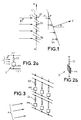
- Such a panel comprises (see FIG. 1) several phase-shifting elements each consisting of a diode D1 to D4.
- Each diode is controlled by control wires such as L1 and L'1 for the diode D1.
- control wires such as L1 and L'1 for the diode D1.
- the diodes and the connection wires connecting them to the control wires are aligned in a direction XX 'so that the direction of the electric field E of an electromagnetic H wave to be processed by the phase shift panel is parallel to this direction XX '.
- the control wires make it possible to conduct or block each diode individually. It is shown that in the blocked state, the diodes present, at an incident wave, a capacitive circuit. On the other hand, in the on state, they have an impedance comprising an inductance. Different diode circuits therefore make it possible to induce different phase shifts on an incident wave. By adjusting these phase shifts according to a determined law (a progression for example), it is possible to obtain a deflection of the beam passing through the diode assembly. This is what is shown diagrammatically in FIG. 1 where the resulting wavefront has been deviated by an angle a and therefore the direction of propagation of the wave E 'is deviated by an angle 0.
- the invention overcomes the problems of connectors related to the control of the diodes.
- a phase shifting element comprises a photoconductive element which, when illuminated by an optical beam, is made conductive.
- FIG. 2 represents such a phase-shifting element comprising a conductive element CO and a photoconductive element PH.
- the photoconductive element is capable of being made conductive by the beam O.
- the conductive element CO is oriented in a determined direction and the direction of propagation of the electromagnetic wave H is not collinear with the direction of orientation of the CO element.
- the conductive element CO is oriented parallel to the electric field E of the electromagnetic wave H to be treated.
- connection wires L1, L'1 contained in the same plane as the conductive element CO and perpendicular to this conductive element. These connection wires L1, L'1 make it possible to connect the phase-shifting element to a voltage source or to a load impedance not shown.
- phase-shifting panel is done as shown in FIG. 3, by combining in parallel between conductors A1, A'1 phase-shifting elements. Several lines of phase shifting elements are thus arranged on the path of the electromagnetic wave H.
- the invention provides for selectively controlling each photoconductive element PH by an optical beam O.
- the phase-shifting element may comprise almost only the photoconductive element which is then preferably of elongated shape.
- the photoconductive element is made of semiconductor material.
- the semiconductor Under illumination of an optical radiation, there is creation in the semiconductor of a number of photocarriers which locally is given by the formula:
- This formula is local, in the sense that it only concerns an area whose dimensions are much smaller than the diffusion length of the carriers, and the optical absorption length.
- the number of photocreated carriers can be 5.10 16 / cm 3 .
- the skin depth is given by the formula (fn) 2 to 10 GH for a number of carriers of 10 21 the skin depth is 0.3 wm, for 100 GHz, it is 0.03 ⁇ m for the same number of electrons. For 5 10 16 carriers; the skin depth will be 5 ⁇ m.
- FIG. 2b represents an alternative embodiment according to which the surface of the photoconductor receiving the optical beam O is etched in the form of an array to form a polarizer.
- a phase-shifting panel as shown in FIG. 3 is in the form of a grid, each phase-shifting element of which has a half wavelength dimension.
- the configuration of such a grid defines the coupling mode (capacitive or inductive) with the hyper wave.
- each phase-shifting element comprises a photoconductive element and a conductive element.
- the switching properties of the photoconductor are mainly used here.
- the lens (or the phase plane) is preconfigured using metal segments, the photoconductive zones are located at the interconnections, they are possibly delimited to take account of the diffusion of the carriers.
- the use of an electronic switching point makes it possible to integrate memory functions (flip-flop, point Si c memory) this possibility makes it possible to envisage the impulse operation of the light source and a scanning with two orthogonal mirrors to scan a laser.
- the invention also provides for associating an electroluminescent memory point with a photoconductor and using the bistability of this system (reset to zero by removing the voltage).
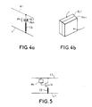
- phase shifting element is then as shown in FIGS. 5a and 5b.
- a photoconductive element PH comprises a photoconductive element PH1 and an electroluminescent element EL1.
- a permanent control voltage V is applied to the conductors A1 andnl.
- the photoconductive element PH1 When the photoconductive element PH1 is illuminated, its resistance decreases. The voltage across the EL1 electroluminescent element increases. The electroluminescent element EL1 emits light which illuminates the photoconductive element PH1 and which then keeps its resistance value low.
- the phase shifting element such as that of FIG. 5a, remains in the controlled situation. To return it to the initial position, it suffices to delete the control voltage V.
- Such a device can be controlled by a light pulse, the duration of which need only be sufficient to control the electroluminescent element.
- FIG. 5c represents a phase-shifting element comprising a transistor Tr, the control circuit of which comprises a photoconductive element PH.
- a microwave line is in series with the transistor Tr.
- phase-shifting elements of a phase-shifting panel can be produced on one face 10 of a dielectric plate DI (FIG. 6a). This plate is transparent to microwave waves and the phase shift panel operates in transmission.
- the face 11 can also support any other means of reflection, other than a metallization ME, such as a reflection network (network of metallic wires).
- a reflection network network of metallic wires
- Figure 6c shows another alternative embodiment according to which the face 11 supports a second phase-shifting panel. This allows either to increase the phase shift combinations, the microwave wave successively seeing two layers of phase shifting elements; or to provide the phase-shifting panel of the face 10 to phase-shift an electric field oriented in one direction and the phase-shifting panel of the face 11 to phase-shift the orthogonal electric field.
- a phase shifting element can also consist of a stack of several photoconductive elements.
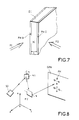
- FIG. 7 represents a phase-shifting element comprising on either side of a support DI (dielectric for example) of the photoconductive PHI and PHII layers.
- the thickness of the DI support is provided equal to a microwave half-length to be treated.
- Such an element can be optically controlled by beams FI, FII coming from sources located on either side of the phase shifter element. It can also be controlled by beams from sources located on the same side with respect to the phase shifting element, the DI support then being transparent to optical control waves.
- the device according to the invention is optically controlled, when several phase-shifting elements are deposited to form a phase-shifting panel, it is advisable to provide a system for selectively controlling each phase-shifting element.
- the addressing of the different points can be done on the different photoconductive switching points using a double vertical and horizontal scanning system (mirrors, XY photoacoustic or electrooptic deflectors). It is then possible to provide a controllable storage function near the switching point.
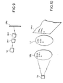
- the laser SO illuminates a first mirror M1 movable around an axis of rotation parallel to an axis OX.
- the light is reflected on a second M2 movable mirror around an axis of rotation parallel to an OY axis perpendicular to the OX axis.
- the phase shift panel DPH is located parallel to the axis OXY so that the beam from the SO laser scans the entire surface of the phase shift panel.
- the mirrors M1 and M2 can also be produced in the form of photoacoustic deflectors DA1, DA2 which make it possible to explore the phase-shifting panel at a rate of 10 ns per point for example. These deflectors are shown in Figure 9.
- FIG. 10 shows an addressing system using a spatial light modulator MSL
- this modulator comprises a set of elementary modulators which can be individually controlled.
- each elementary modulator makes it possible, according to the command it receives, to retransmit all or part of the light coming from the source SO, to a determined zone of the phase-shifting panel DPH and in particular to a particular phase-shifting element of the phase-shifting panel.
- each element of the MSL spatial modulator is associated with an element of the phase shift panel.
- the MSL spatial modulator is a liquid crystal screen which thus makes it possible to display the control state of the phase shift panel.
- the dimensions of the spatial light modulator could be 50 x 50 mm, as could the phase shift panel.
- Each of these devices may consist of 100 x 100 elements of dimensions 0.5 x 0.5 mm approximately.
- the lens array can be realized in holography.
- the optical power required to switch a photoconductor is more directly accessible by direct laser impact.
- the direct addressing of an element to be made conductive, for example using photoacoustic deflectors can be limited in number of points and in precision.
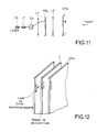
- the solution shown in FIG. 11 solves these problems, because it uses a spatial modulator MSL as a reconfigurable mask projected on the lens network L2. Photoacoustic deflection used only to deflect the laser beam. This solution requires the integration of a memory function at the photoconductive pixel level.
- the system of FIG. 11 comprises a cylindrical lens L1 making it possible to illuminate, using the source SO, the electroacoustic deflector DA which performs a deflection in an X or Y direction.
- a lens L3 makes it possible to increase the divergence of the scanning acousto-optics.
- the MSL spatial modulator is thus swept by a light sheet whose deflection can be rapid.
- a L2 concentration lens or a lens array focuses the beams from the MLS modulator on the DPH phase shifting panel.
- the lighting system of the phase shift panel can comprise an array of lasers emitting from the surface.
- the powers can be 10 5 W / cm 2 with a small angle of divergence (1 degree for example).
- Such a system does not require lenses. This situation is favorable for lighting the photoconductor from the front face.
- the attack voltage is of the order of a volt, ie a hundred Watts in the worst case.
- the invention can advantageously be applied to antennas with electronic scanning in the millimeter and submillimetric range.
- the invention has as an application the production of antennae with electronic scanning in reflection.
- These antennas are in the form of a thin metallized dielectric layer on one side, and etched with periodic patterns on the other side.
- the elementary pattern is formed by an iris phase shifter in a short-circuited thin guide; the guide being formed by lines of metallized holes (the latter condition not always being necessary).
- the losses of the phase shifter being a function of the microwave resistance when the photodiodes are conductive and the tangent of silicon leakage when the photodiodes are not conductive:
- the other two parameters necessary for the phase shifter settings are the iris capacity and the self.
- Networking therefore makes it possible to constitute an antenna with electronic scanning in reflection.
- the short-circuit plane is replaced by a network of "tight" continuous wires with a pitch of ⁇ g / 10, which corresponds substantially to a distance of 100 ⁇ m.
- a microwave source corresponds to a monopulsed horn and placed at a distance F / D - - 1 (F distance from the source, D dimension of the lens).
- the "optically” controlled lens allows the focusing of the wave and the deflection of the wave over an angular opening corresponding to a 120 ° cone, the spacing between sources being very close to ⁇ 2 ( ⁇ in air).
- the antenna can be bipolarized, by replacing the iris pattern, with a generalized pattern as shown in FIG. 14.
- Each phase-shifting element has four photoconductive elements Di1, Di'1, Di2, Di'2. These elements are produced on one face of a substrate. Each element such as Di1 is connected to conductive pads C1, C'l which allow connections to be made through the substrate to conductors located on the other face of the substrate and equivalent to the conductors L1, L'1 in FIG. 1 .
- the elements Di1, Di'1 make it possible to process a component of the direction of polarization of the microwave wave.
- the elements Di2, Di'2 make it possible to process the orthogonal component of the direction of polarization.
- the central element EC is a capacitive adaptation element.
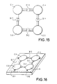
- Figures 15 and 16 show an alternative embodiment of the phase shifter of Figure 14.
- a conductive pad is common to two photoconductive elements, the pad Ci1 is common to the elements Di'1 and Di'2 for example, the pad Ci2 for the elements Di'1 and Di2, etc ...
- Each interconnection is connected to one end of a load impedance, or to conductors such as conductors L1 and L'1 in FIG. 2a.
Landscapes
- Variable-Direction Aerials And Aerial Arrays (AREA)
Applications Claiming Priority (2)
| Application Number | Priority Date | Filing Date | Title |
|---|---|---|---|
| FR9213019A FR2697679B1 (fr) | 1992-10-30 | 1992-10-30 | Déphaseur d'ondes électromagnétiques et application à une antenne à balayage électronique. |
| FR9213019 | 1992-10-30 |
Publications (1)
| Publication Number | Publication Date |
|---|---|
| EP0595726A1 true EP0595726A1 (de) | 1994-05-04 |
Family
ID=9435031
Family Applications (1)
| Application Number | Title | Priority Date | Filing Date |
|---|---|---|---|
| EP93402667A Withdrawn EP0595726A1 (de) | 1992-10-30 | 1993-10-29 | Phasenschieber für elektromagnetische Wellen und Verwendung in einer Antenne mit elektronischer Ablenkung |
Country Status (2)
| Country | Link |
|---|---|
| EP (1) | EP0595726A1 (de) |
| FR (1) | FR2697679B1 (de) |
Cited By (11)
| Publication number | Priority date | Publication date | Assignee | Title |
|---|---|---|---|---|
| GB2280988A (en) * | 1993-08-06 | 1995-02-15 | Thomson Csf Radant | A phase shifter panel for an electronic scanning antenna |
| WO1996014670A1 (en) * | 1994-11-04 | 1996-05-17 | Deltec New Zealand Limited | An antenna control system |
| EP1133000A1 (de) * | 2000-03-07 | 2001-09-12 | Thomson-Csf | Aktiver Mikrowellenreflektor für Antenne mit elektronischer Strahlschwenkung |
| US6313804B1 (en) | 1998-12-03 | 2001-11-06 | Telefonaktiebolaget Lm Ericsson (Publ) | Continuous aperture scanning antenna |
| US6573875B2 (en) | 2001-02-19 | 2003-06-03 | Andrew Corporation | Antenna system |
| FR2834131A1 (fr) * | 2001-12-21 | 2003-06-27 | Thales Sa | Panneau dephaseur monolithique a diodes pin en silicium polycristallin et antenne utilisant ce panneau dephaseur |
| US6677896B2 (en) | 1999-06-30 | 2004-01-13 | Radio Frequency Systems, Inc. | Remote tilt antenna system |
| US7031751B2 (en) | 2001-02-01 | 2006-04-18 | Kathrein-Werke Kg | Control device for adjusting a different slope angle, especially of a mobile radio antenna associated with a base station, and corresponding antenna and corresponding method for modifying the slope angle |
| EP1972882A1 (de) | 2007-03-21 | 2008-09-24 | Dassault Aviation | Elektromagnetisches Fenster |
| US7557675B2 (en) | 2005-03-22 | 2009-07-07 | Radiacion Y Microondas, S.A. | Broad band mechanical phase shifter |
| WO2012100885A1 (en) * | 2011-01-25 | 2012-08-02 | Sony Corporation | Optically controlled microwave antenna |
Citations (3)
| Publication number | Priority date | Publication date | Assignee | Title |
|---|---|---|---|---|
| US3979750A (en) * | 1975-06-20 | 1976-09-07 | The United States Of America As Represented By The Secretary Of The Army | Optical pump power distribution feed |
| JPS57107607A (en) * | 1980-12-25 | 1982-07-05 | Toshiba Corp | Array antenna device |
| EP0248686A1 (de) * | 1986-04-22 | 1987-12-09 | Thomson-Csf | Gruppe von Elementen, die elektromagnetische Energie bei optischer Steuerung aussenden |
-
1992
- 1992-10-30 FR FR9213019A patent/FR2697679B1/fr not_active Expired - Fee Related
-
1993
- 1993-10-29 EP EP93402667A patent/EP0595726A1/de not_active Withdrawn
Patent Citations (3)
| Publication number | Priority date | Publication date | Assignee | Title |
|---|---|---|---|---|
| US3979750A (en) * | 1975-06-20 | 1976-09-07 | The United States Of America As Represented By The Secretary Of The Army | Optical pump power distribution feed |
| JPS57107607A (en) * | 1980-12-25 | 1982-07-05 | Toshiba Corp | Array antenna device |
| EP0248686A1 (de) * | 1986-04-22 | 1987-12-09 | Thomson-Csf | Gruppe von Elementen, die elektromagnetische Energie bei optischer Steuerung aussenden |
Non-Patent Citations (3)
| Title |
|---|
| JEMISON ET AL.: "OPTICAL CONTROL OF A DIGITAL PHASE SHIFTER", 1990 IEEE MTT-S INTERNATIONAL MICROWAVE SYMPOSIUM DIGEST, vol. I, May 1990 (1990-05-01), DALLAS,TEXAS, pages 233 - 236 * |
| PARK: "Radant Lens: Alternative to Expensive Phased Arrays", MICROWAVE JOURNAL., vol. 24, no. 9, September 1981 (1981-09-01), DEDHAM US, pages 101 - 105, XP001386995 * |
| PATENT ABSTRACTS OF JAPAN vol. 6, no. 200 (E - 135)<1078> 9 October 1982 (1982-10-09) * |
Cited By (23)
| Publication number | Priority date | Publication date | Assignee | Title |
|---|---|---|---|---|
| GB2280988B (en) * | 1993-08-06 | 1997-04-30 | Thomson Csf Radant | A phase shifter panel and its application to a microwave lens and to an electronic scanning antenna |
| GB2280988A (en) * | 1993-08-06 | 1995-02-15 | Thomson Csf Radant | A phase shifter panel for an electronic scanning antenna |
| US6600457B2 (en) | 1994-11-04 | 2003-07-29 | Andrew Corporation | Antenna control system |
| WO1996014670A1 (en) * | 1994-11-04 | 1996-05-17 | Deltec New Zealand Limited | An antenna control system |
| US6198458B1 (en) | 1994-11-04 | 2001-03-06 | Deltec Telesystems International Limited | Antenna control system |
| US8558739B2 (en) | 1994-11-04 | 2013-10-15 | Andrew Llc | Antenna control system |
| US6346924B1 (en) | 1994-11-04 | 2002-02-12 | Andrew Corporation | Antenna control system |
| US6538619B2 (en) | 1994-11-04 | 2003-03-25 | Andrew Corporation | Antenna control system |
| US6567051B2 (en) | 1994-11-04 | 2003-05-20 | Andrew Corporation | Antenna control system |
| US6603436B2 (en) | 1994-11-04 | 2003-08-05 | Andrew Corporation | Antenna control system |
| US6590546B2 (en) | 1994-11-04 | 2003-07-08 | Andrew Corporation | Antenna control system |
| US6313804B1 (en) | 1998-12-03 | 2001-11-06 | Telefonaktiebolaget Lm Ericsson (Publ) | Continuous aperture scanning antenna |
| US6677896B2 (en) | 1999-06-30 | 2004-01-13 | Radio Frequency Systems, Inc. | Remote tilt antenna system |
| EP1133000A1 (de) * | 2000-03-07 | 2001-09-12 | Thomson-Csf | Aktiver Mikrowellenreflektor für Antenne mit elektronischer Strahlschwenkung |
| US7031751B2 (en) | 2001-02-01 | 2006-04-18 | Kathrein-Werke Kg | Control device for adjusting a different slope angle, especially of a mobile radio antenna associated with a base station, and corresponding antenna and corresponding method for modifying the slope angle |
| US6573875B2 (en) | 2001-02-19 | 2003-06-03 | Andrew Corporation | Antenna system |
| US6987487B2 (en) | 2001-02-19 | 2006-01-17 | Andrew Corporation | Antenna system |
| WO2003056659A1 (fr) * | 2001-12-21 | 2003-07-10 | Thales | Panneau dephaseur monolithique |
| FR2834131A1 (fr) * | 2001-12-21 | 2003-06-27 | Thales Sa | Panneau dephaseur monolithique a diodes pin en silicium polycristallin et antenne utilisant ce panneau dephaseur |
| US7557675B2 (en) | 2005-03-22 | 2009-07-07 | Radiacion Y Microondas, S.A. | Broad band mechanical phase shifter |
| EP1972882A1 (de) | 2007-03-21 | 2008-09-24 | Dassault Aviation | Elektromagnetisches Fenster |
| WO2012100885A1 (en) * | 2011-01-25 | 2012-08-02 | Sony Corporation | Optically controlled microwave antenna |
| US9496610B2 (en) | 2011-01-25 | 2016-11-15 | Sony Corporation | Optically controlled microwave antenna |
Also Published As
| Publication number | Publication date |
|---|---|
| FR2697679B1 (fr) | 1994-11-25 |
| FR2697679A1 (fr) | 1994-05-06 |
Similar Documents
| Publication | Publication Date | Title |
|---|---|---|
| US10084239B2 (en) | RF diffractive element with dynamically writable sub-wavelength pattern spatial definition | |
| EP0237429B1 (de) | Phasengesteuerte Reflektorstrahlergruppe und Antenne mit einer solchen Gruppe | |
| CA2148796C (fr) | Antenne fil-plaque monopolaire | |
| EP1387437A1 (de) | Gruppenantenne für eine Reflektoranordnung | |
| WO1981001486A1 (fr) | Dispositif de balayage electronique dans le plan de polarisation | |
| FR2725077A1 (fr) | Lentille hyperfrequence bipolarisation et son application a une antenne a balayage electronique | |
| FR2697679A1 (fr) | Déphaseur d'ondes électromagnétiques et application à une antenne à balayage électronique. | |
| EP4189772B1 (de) | Metaoberflächenvorrichtung | |
| EP0519772B1 (de) | Mikrowellenantenne mit optoelektronisch gesteuertem Absuchen | |
| WO2022023126A1 (fr) | Dispositif a metasurface | |
| EP1305846B1 (de) | Doppelpolarisierter aktiver mikrowellenreflektor, insbesondere für antenne mit elektronischer strahlschwenkung | |
| EP0548876B1 (de) | Asymmetrische Spiegelantenne mit zwei Reflektoren | |
| EP0435739B1 (de) | Magische Mikrowellenquelle und ihre Anwendung bei einer Antenne mit elektronischem Absuchen | |
| EP4523291B1 (de) | Flache antenne mit zweidimensionaler elektronischer abtastung | |
| EP1234356A1 (de) | Aktiver hf reflektor unter verwendung von elektronischer strahlschenkung | |
| EP4350890A1 (de) | Schalter auf basis eines phasenwechselmaterials | |
| FR2512280A1 (fr) | Panneau commutateur spatial hyperfrequence et procede de mise en oeuvre d'un tel panneau | |
| EP1157444B1 (de) | Antenne mit doppelbandiger elektronischerabtastung mit aktivem mirkowellenrefkelektor | |
| EP0432034A1 (de) | Vorrichtung zur räumlich selektiven Absorption elektromagnetischer Wellen für eine Linse im ultrahohen Frequenzbereich | |
| FR2747842A1 (fr) | Lentille hyperfrequence multibande et son application a une antenne a balayage electronique | |
| FR2679703A1 (fr) | Dispositif hyperfrequence a semiconducteur et a commande optique. | |
| FR2690583A1 (fr) | Relais de transmission pour guidage ou sélection de faisceau. | |
| EP1133000B1 (de) | Aktiver Mikrowellenreflektor für Antenne mit elektronischer Strahlschwenkung | |
| FR2522888A1 (fr) | Antenne a double reflecteur a transformateur de polarisation incorpore | |
| FR2890792A1 (fr) | Element d'antenne reseau et antenne reseau a balayage electronique par reflexion et procede de realisation de cet element |
Legal Events
| Date | Code | Title | Description |
|---|---|---|---|
| PUAI | Public reference made under article 153(3) epc to a published international application that has entered the european phase |
Free format text: ORIGINAL CODE: 0009012 |
|
| AK | Designated contracting states |
Kind code of ref document: A1 Designated state(s): DE GB |
|
| STAA | Information on the status of an ep patent application or granted ep patent |
Free format text: STATUS: THE APPLICATION IS DEEMED TO BE WITHDRAWN |
|
| 18D | Application deemed to be withdrawn |
Effective date: 19941105 |