EP0596169B1 - Circuit et procédé pour la fabrication d'un filtre à bande étroite et haut facteur de qualité - Google Patents
Circuit et procédé pour la fabrication d'un filtre à bande étroite et haut facteur de qualité Download PDFInfo
- Publication number
- EP0596169B1 EP0596169B1 EP92310174A EP92310174A EP0596169B1 EP 0596169 B1 EP0596169 B1 EP 0596169B1 EP 92310174 A EP92310174 A EP 92310174A EP 92310174 A EP92310174 A EP 92310174A EP 0596169 B1 EP0596169 B1 EP 0596169B1
- Authority
- EP
- European Patent Office
- Prior art keywords
- filter
- circuit
- filter circuit
- psk3
- psk1
- Prior art date
- Legal status (The legal status is an assumption and is not a legal conclusion. Google has not performed a legal analysis and makes no representation as to the accuracy of the status listed.)
- Expired - Lifetime
Links
Images
Classifications
-
- H—ELECTRICITY
- H03—ELECTRONIC CIRCUITRY
- H03H—IMPEDANCE NETWORKS, e.g. RESONANT CIRCUITS; RESONATORS
- H03H9/00—Networks comprising electromechanical or electro-acoustic elements; Electromechanical resonators
- H03H9/46—Filters
- H03H9/54—Filters comprising resonators of piezoelectric or electrostrictive material
- H03H9/542—Filters comprising resonators of piezoelectric or electrostrictive material including passive elements
-
- H—ELECTRICITY
- H03—ELECTRONIC CIRCUITRY
- H03H—IMPEDANCE NETWORKS, e.g. RESONANT CIRCUITS; RESONATORS
- H03H7/00—Multiple-port networks comprising only passive electrical elements as network components
- H03H7/01—Frequency selective two-port networks
- H03H7/03—Frequency selective two-port networks comprising means for compensation of loss
-
- H—ELECTRICITY
- H03—ELECTRONIC CIRCUITRY
- H03H—IMPEDANCE NETWORKS, e.g. RESONANT CIRCUITS; RESONATORS
- H03H7/00—Multiple-port networks comprising only passive electrical elements as network components
- H03H7/01—Frequency selective two-port networks
- H03H7/075—Ladder networks, e.g. electric wave filters
-
- H—ELECTRICITY
- H03—ELECTRONIC CIRCUITRY
- H03H—IMPEDANCE NETWORKS, e.g. RESONANT CIRCUITS; RESONATORS
- H03H7/00—Multiple-port networks comprising only passive electrical elements as network components
- H03H7/01—Frequency selective two-port networks
- H03H7/17—Structural details of sub-circuits of frequency selective networks
- H03H7/1741—Comprising typical LC combinations, irrespective of presence and location of additional resistors
- H03H7/175—Series LC in series path
-
- H—ELECTRICITY
- H03—ELECTRONIC CIRCUITRY
- H03H—IMPEDANCE NETWORKS, e.g. RESONANT CIRCUITS; RESONATORS
- H03H7/00—Multiple-port networks comprising only passive electrical elements as network components
- H03H7/01—Frequency selective two-port networks
- H03H7/17—Structural details of sub-circuits of frequency selective networks
- H03H7/1741—Comprising typical LC combinations, irrespective of presence and location of additional resistors
- H03H7/1775—Parallel LC in shunt or branch path
Definitions
- the invention relates to a manufacturing method and Circuit arrangement for a narrow-band filter of high quality according to the preamble of claims 1 and 3.
- Narrow band filters of high quality e.g. B. designed as a quartz filter
- Intermediate frequency filters are used in particular there where frequency components in analog signal transmission can be suppressed for a single-channel or multi-channel system have to.
- Cordless communication is one such case according to the CT1 + standard.
- wireless communication one operated according to this standard Cordless communication system consisting of at least one Mobile station and base station, is used for the direction of transmission "Mobile station - base station" an MS / BS analog signal with an MS / BS signal frequency of 886 MHz and for the Transmission direction "base station - mobile station" BS / MS analog signal with a BS / MS signal frequency of 931 MHz transfer.
- a respective Receiving device the base station for the MS-BS transmission direction and the mobile station for the BS-MS transmission direction
- one mixer each provided by a Controlled oscillator, from the respectively received analog signal a first with the associated signal frequency and second output signal generated.
- the first output signal has a frequency that is the sum of the signal frequency of the analog signal and an oscillator frequency of an oscillator signal results.
- the second output signal that also as the working signal of the intermediate frequency filter or Quartz filter has a frequency that from the absolute difference between the signal frequency of the analog signal and the oscillator frequency of the oscillator signal results.
- these two signals contains only the analog signal from the mobile station or base station transmitted information.
- base station - mobile station this means that the analog signal with the signal frequency of 931 MHz based on the oscillator signal with the oscillator frequency of 989 MHz serves as an information carrier and that to this analog signal (carrier signal) based on the oscillator frequency suppresses the further signal with the image frequency must become.
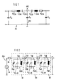
- FIG. 1 shows the equivalent circuit diagram of a filter circuit FS designed as a quartz filter.
- the filter circuit FS is shown as a four-pole, which is symmetrical to a parallel capacitor C P arranged in a main parallel branch HPZ in two four-pole branches VPZ, which form a T arrangement with the main parallel branch HPZ, each a series circuit SSK, consisting of a resistor R SSK , one Coil L SSK and a capacitor C SSK , has.
- a terminating capacitor C A is arranged at each of the two outputs of the filter circuit FS shown as a four-pole circuit in parallel with an overall resonant circuit consisting of the series resonant circuit SSK and the parallel capacitor C P.
- the termination capacitor C A takes z.
- B various parasitic interference / stray capacitances impairing the filter characteristic of the filter circuit FS.
- the filter circuit FS according to FIG. 1 is expanded to a filter circuit arrangement FSA according to FIG. 2.
- the filter circuit arrangement FSA is here, in order to represent the conditions described at the outset when the analog signal is received in the base or mobile station of the cordless communication system, on the input side to a signal generator SG with an internal resistance Ri and on the output side to a load (consumer) L.
- the filter circuit arrangement FSA contains, for example, a first filter circuit FS1 and a second filter circuit FS2, which are connected in series with one another.
- the first filter circuit FS1 is assigned a first parallel resonant circuit PSK1 which is connected in parallel with the filter circuit FS1 and which forms an input circuit EK with the first filter circuit FS1.
- the second filter circuit FS2 is assigned a second parallel resonant circuit PSK2 which is connected in parallel and which forms an output circuit AK with the second filter circuit FS2.
- the two filter circuits FS1, FS2 are assigned a third parallel resonant circuit PSK3 which is connected in parallel and which forms a coupling circuit KK with the two filter circuits FS1, FS2.
- the parallel resonant circuits PSK1 ...
- PSK3 connected in parallel to the filter circuits FS1, FS2 are required in order to compensate for the interference / stray capacitances taken into account in the terminating capacitors C A of the filter circuits FS1, FS2 (as shown in FIG. 1).
- the coupling circuit KK and the output circuit AK further parasitic physical quantities, such as. B. Line reactances (line capacities, line inductances) to compensate are in the parallel resonant circuits PSK1 ...
- the object of the invention is a manufacturing method and a circuit arrangement for a narrow-band filter high Indicate quality in which no adjustment procedures are to be carried out are.
- This task is based on that in the preamble of Claim 1 defined manufacturing process by that specified in the characterizing part of claim 1 Characteristics as well as starting from that in the preamble of claim 5 defined circuit arrangement by the specified in the characterizing part of claim 5 Features resolved.
- the invention consists in the fact that in FIGS shown line connections measured with a Meßanordnng and then when choosing the one in the parallel resonant circuits PSK1 ... PSK3 used capacitors and Coils are taken into account. Through this procedure it is possible that no changeable capacitors, coils in the parallel resonant circuits PSK1 ... PSK3 are necessary (no adjustment points or procedures).
Landscapes
- Physics & Mathematics (AREA)
- Acoustics & Sound (AREA)
- Filters And Equalizers (AREA)
- Networks Using Active Elements (AREA)
- Measurement Of Resistance Or Impedance (AREA)
- Control Of Motors That Do Not Use Commutators (AREA)
- Nitrogen Condensed Heterocyclic Rings (AREA)
Claims (7)
- Procédé de fabrication d'un filtre à bande étroite ayant un haut facteur de qualité, dans lequel
un circuit de filtrage (FS1, FS2) et un circuit de filtrage de compensation (PSK1 à PSK3) sont associés au filtre, plusieurs composants déterminant la caractéristique de filtrage étant associés au circuit de filtrage (FS1, FS2) et au circuit de filtrage de compensation (PSK1 à PSK3), et dans lequel les composants du circuit de filtrage (FS1, FS2) et du circuit de filtrage de compensation (PSK1 à PSK3) sont reliés entre eux,
caractérisé par le fait qu'on mesure les liaisons entre les composants pour ce qui concerne des grandeurs physiques parasites influençant la caractéristique de filtrage et qu'on prend en compte les grandeurs physiques parasites déterminées par la mesure lors de la conception du circuit de filtrage de compensation (PSK1 à PSK3) avec les composants associés à celui-ci. - Procédé de fabrication selon la revendication 1,
caractérisé par le fait qu'on mesure des capacités de dispersion ou des inductances de dispersion en tant que grandeurs physiques parasites influençant la caractéristique de filtrage. - Procédé de fabrication selon la revendication 1 ou 2,
caractérisé par le fait qu'on n'associe au circuit de filtrage de compensation (PSK1 à PSK3) que des composants ayant une valeur prédéterminée constante pour une grandeur physique attribuée au composant. - Procédé de fabrication selon la revendication 3,
caractérisé par le fait qu'on attribue au composant du circuit de filtrage de compensation (PSK1 à PSK3) la capacité, l'inductance ou la résistance en tant que grandeur physique. - Montage pour un filtre à bande étroite ayant un haut facteur de qualité, comportant au moins un circuit de filtrage (FS1, FS2) et au moins un circuit de filtrage de compensation (PSK1 à PSK3), plusieurs composants qui déterminent la caractéristique de filtrage et qui sont reliés entre eux étant associés à chaque fois au circuit de filtrage (FS1, FS2) et au circuit de filtrage de compensation (PSK1 à PSK3),
caractérisé par le fait que les composants du circuit de filtrage de compensation (PSK1 à PSK3) sont conçus sous forme de composants non variables pour lesquels des grandeurs physiques parasites influençant la caractéristique de filtrage et déterminées par la mesure des liaisons entre les composants sont prises en compte. - Montage selon la revendication 5,
caractérisé par le fait que le circuit de filtrage (FS1, FS2) est conçu sous forme de filtre à quartz. - Montage selon la revendication 5 ou 6,
caractérisé par le fait que le circuit de filtrage de compensation (PSK1 à PSK3) est conçu sous forme de circuit oscillant parallèle.
Priority Applications (5)
| Application Number | Priority Date | Filing Date | Title |
|---|---|---|---|
| DE59209411T DE59209411D1 (de) | 1992-11-06 | 1992-11-06 | Herstellungsverfahren und Schaltungsanordnung für ein schmalbandiges Filter hoher Güte |
| AT92310174T ATE168231T1 (de) | 1992-11-06 | 1992-11-06 | Herstellungsverfahren und schaltungsanordnung für ein schmalbandiges filter hoher güte |
| EP92310174A EP0596169B1 (fr) | 1992-11-06 | 1992-11-06 | Circuit et procédé pour la fabrication d'un filtre à bande étroite et haut facteur de qualité |
| ES92310174T ES2119801T3 (es) | 1992-11-06 | 1992-11-06 | Procedimiento de fabricacion y disposicion de conexion para un filtro de banda estrecha de alta calidad. |
| FI934912A FI934912A7 (fi) | 1992-11-06 | 1993-11-05 | Valmistumenetelmä ja piirijärjestely suuren hyvyyden kapeakaistaista suodatinta varten |
Applications Claiming Priority (1)
| Application Number | Priority Date | Filing Date | Title |
|---|---|---|---|
| EP92310174A EP0596169B1 (fr) | 1992-11-06 | 1992-11-06 | Circuit et procédé pour la fabrication d'un filtre à bande étroite et haut facteur de qualité |
Publications (2)
| Publication Number | Publication Date |
|---|---|
| EP0596169A1 EP0596169A1 (fr) | 1994-05-11 |
| EP0596169B1 true EP0596169B1 (fr) | 1998-07-08 |
Family
ID=8211547
Family Applications (1)
| Application Number | Title | Priority Date | Filing Date |
|---|---|---|---|
| EP92310174A Expired - Lifetime EP0596169B1 (fr) | 1992-11-06 | 1992-11-06 | Circuit et procédé pour la fabrication d'un filtre à bande étroite et haut facteur de qualité |
Country Status (5)
| Country | Link |
|---|---|
| EP (1) | EP0596169B1 (fr) |
| AT (1) | ATE168231T1 (fr) |
| DE (1) | DE59209411D1 (fr) |
| ES (1) | ES2119801T3 (fr) |
| FI (1) | FI934912A7 (fr) |
Family Cites Families (1)
| Publication number | Priority date | Publication date | Assignee | Title |
|---|---|---|---|---|
| US3185943A (en) * | 1956-04-23 | 1965-05-25 | Toyotsushinki Kabushiki Kaisha | One-piece mechanical filter having portions forming plural resonators and coupling means |
-
1992
- 1992-11-06 DE DE59209411T patent/DE59209411D1/de not_active Expired - Fee Related
- 1992-11-06 ES ES92310174T patent/ES2119801T3/es not_active Expired - Lifetime
- 1992-11-06 AT AT92310174T patent/ATE168231T1/de not_active IP Right Cessation
- 1992-11-06 EP EP92310174A patent/EP0596169B1/fr not_active Expired - Lifetime
-
1993
- 1993-11-05 FI FI934912A patent/FI934912A7/fi unknown
Non-Patent Citations (1)
| Title |
|---|
| LU S. K. S.: "DESIGN OF SYMMETRICAL POLYLITHIC CRYSTAL FILTERS HAVING EQUAL MOTIONAL INDUCTANCES.", ELECTRONICS LETTERS, IEE STEVENAGE., GB, vol. 27., no. 16., 1 August 1991 (1991-08-01), GB, pages 1456 - 1457., XP000259872, ISSN: 0013-5194 * |
Also Published As
| Publication number | Publication date |
|---|---|
| EP0596169A1 (fr) | 1994-05-11 |
| FI934912A0 (fi) | 1993-11-05 |
| ES2119801T3 (es) | 1998-10-16 |
| FI934912L (fi) | 1994-05-07 |
| FI934912A7 (fi) | 1994-05-07 |
| ATE168231T1 (de) | 1998-07-15 |
| DE59209411D1 (de) | 1998-08-13 |
Similar Documents
| Publication | Publication Date | Title |
|---|---|---|
| DE69216554T2 (de) | Verfahren und Einrichtung zur automatischen Abstimmkalibrierung von elektronisch abgestimmten Filtern | |
| DE3850729T2 (de) | Monolithischer integrierter Mikrowellenverstärker. | |
| DE3832293C2 (de) | Anpassungsschaltung | |
| EP1547245A2 (fr) | Montage filtrant | |
| DE2114056C3 (de) | Abstimmeinrichtung | |
| DE102008059157A1 (de) | Differenzielles Bandpassfilter mit symmetrisch verflochtenen Induktivitäten | |
| DE102009009484A1 (de) | SAW Filter | |
| DE2536496C3 (de) | Fernsehempfänger-Schaltungsanordnung zum Trennen des Helligkeitssignals vom Tonsignal | |
| DE3606437C2 (fr) | ||
| DE102004053319A1 (de) | Frequenzweiche | |
| EP0596169B1 (fr) | Circuit et procédé pour la fabrication d'un filtre à bande étroite et haut facteur de qualité | |
| DE3606438C2 (fr) | ||
| DE10344167B3 (de) | Verfahren und Vorrichtung zur Einstellung eines Filters | |
| EP1875607A2 (fr) | Filtre d'entree permettant la suppression de la frequence-image | |
| DE4014407C2 (fr) | ||
| DE4227833C2 (de) | Zwischenfrequenzfilter für einen Funkempfänger | |
| DE3205875C2 (de) | Einstellbare Entzerrerschaltung | |
| DE2748559A1 (de) | Laufzeitenzerrer fuer geraete der elektrischen nachrichtentechnik | |
| DE2321462C3 (de) | Bandpaßfilter für den Rundfunk- und Fernsehbereich | |
| DE19646774A1 (de) | Verfahren zum Ableich einer HF-Schaltung | |
| DE2065525C3 (de) | Einrichtung zur Einspeisung einer hochfrequenten über ein Parallelkreisfilter ankommenden Signalenergie in eine durchgehende Leitung | |
| DE19703219A1 (de) | Hochfrequenz-Abstimmschaltung | |
| DE2937597C2 (de) | Schaltungsanordnung eines zweikreisigen, gekoppelten Bandfilters | |
| DE3108993A1 (de) | Hf-eingangsfilterschaltung eines tuners | |
| DE876852C (de) | Abstimmbare Bandfilteranordnung fuer konstante absolute Bandbreite |
Legal Events
| Date | Code | Title | Description |
|---|---|---|---|
| PUAI | Public reference made under article 153(3) epc to a published international application that has entered the european phase |
Free format text: ORIGINAL CODE: 0009012 |
|
| AK | Designated contracting states |
Kind code of ref document: A1 Designated state(s): AT BE CH DE DK ES FR GB GR IE IT LI LU MC NL PT SE |
|
| RBV | Designated contracting states (corrected) |
Designated state(s): AT BE CH DE DK ES FR GB IT LI LU NL PT SE |
|
| 17P | Request for examination filed |
Effective date: 19940608 |
|
| K1C1 | Correction of patent application (title page) published |
Effective date: 19940511 |
|
| RIN1 | Information on inventor provided before grant (corrected) |
Inventor name: SMITH, CHRIS N. Inventor name: WEWERS, OTGER Inventor name: EYNOETHEN, PETER |
|
| 17Q | First examination report despatched |
Effective date: 19961202 |
|
| GRAG | Despatch of communication of intention to grant |
Free format text: ORIGINAL CODE: EPIDOS AGRA |
|
| GRAG | Despatch of communication of intention to grant |
Free format text: ORIGINAL CODE: EPIDOS AGRA |
|
| GRAH | Despatch of communication of intention to grant a patent |
Free format text: ORIGINAL CODE: EPIDOS IGRA |
|
| GRAH | Despatch of communication of intention to grant a patent |
Free format text: ORIGINAL CODE: EPIDOS IGRA |
|
| GRAA | (expected) grant |
Free format text: ORIGINAL CODE: 0009210 |
|
| AK | Designated contracting states |
Kind code of ref document: B1 Designated state(s): AT BE CH DE DK ES FR GB IT LI LU NL PT SE |
|
| PG25 | Lapsed in a contracting state [announced via postgrant information from national office to epo] |
Ref country code: NL Free format text: LAPSE BECAUSE OF FAILURE TO SUBMIT A TRANSLATION OF THE DESCRIPTION OR TO PAY THE FEE WITHIN THE PRESCRIBED TIME-LIMIT Effective date: 19980708 |
|
| REF | Corresponds to: |
Ref document number: 168231 Country of ref document: AT Date of ref document: 19980715 Kind code of ref document: T |
|
| REG | Reference to a national code |
Ref country code: CH Ref legal event code: EP |
|
| REF | Corresponds to: |
Ref document number: 59209411 Country of ref document: DE Date of ref document: 19980813 |
|
| GBT | Gb: translation of ep patent filed (gb section 77(6)(a)/1977) |
Effective date: 19980909 |
|
| PG25 | Lapsed in a contracting state [announced via postgrant information from national office to epo] |
Ref country code: SE Free format text: LAPSE BECAUSE OF FAILURE TO SUBMIT A TRANSLATION OF THE DESCRIPTION OR TO PAY THE FEE WITHIN THE PRESCRIBED TIME-LIMIT Effective date: 19981008 Ref country code: PT Free format text: LAPSE BECAUSE OF FAILURE TO SUBMIT A TRANSLATION OF THE DESCRIPTION OR TO PAY THE FEE WITHIN THE PRESCRIBED TIME-LIMIT Effective date: 19981008 Ref country code: DK Free format text: LAPSE BECAUSE OF FAILURE TO SUBMIT A TRANSLATION OF THE DESCRIPTION OR TO PAY THE FEE WITHIN THE PRESCRIBED TIME-LIMIT Effective date: 19981008 |
|
| REG | Reference to a national code |
Ref country code: ES Ref legal event code: FG2A Ref document number: 2119801 Country of ref document: ES Kind code of ref document: T3 |
|
| ET | Fr: translation filed | ||
| PGFP | Annual fee paid to national office [announced via postgrant information from national office to epo] |
Ref country code: GB Payment date: 19981026 Year of fee payment: 7 |
|
| PG25 | Lapsed in a contracting state [announced via postgrant information from national office to epo] |
Ref country code: LU Free format text: LAPSE BECAUSE OF NON-PAYMENT OF DUE FEES Effective date: 19981106 Ref country code: AT Free format text: LAPSE BECAUSE OF NON-PAYMENT OF DUE FEES Effective date: 19981106 |
|
| PGFP | Annual fee paid to national office [announced via postgrant information from national office to epo] |
Ref country code: ES Payment date: 19981110 Year of fee payment: 7 |
|
| PGFP | Annual fee paid to national office [announced via postgrant information from national office to epo] |
Ref country code: FR Payment date: 19981116 Year of fee payment: 7 |
|
| PG25 | Lapsed in a contracting state [announced via postgrant information from national office to epo] |
Ref country code: LI Free format text: LAPSE BECAUSE OF NON-PAYMENT OF DUE FEES Effective date: 19981130 Ref country code: CH Free format text: LAPSE BECAUSE OF NON-PAYMENT OF DUE FEES Effective date: 19981130 Ref country code: BE Free format text: LAPSE BECAUSE OF NON-PAYMENT OF DUE FEES Effective date: 19981130 |
|
| NLV1 | Nl: lapsed or annulled due to failure to fulfill the requirements of art. 29p and 29m of the patents act | ||
| PGFP | Annual fee paid to national office [announced via postgrant information from national office to epo] |
Ref country code: DE Payment date: 19990120 Year of fee payment: 7 |
|
| PLBE | No opposition filed within time limit |
Free format text: ORIGINAL CODE: 0009261 |
|
| BERE | Be: lapsed |
Owner name: SIEMENS A.G. Effective date: 19981130 |
|
| 26N | No opposition filed | ||
| REG | Reference to a national code |
Ref country code: CH Ref legal event code: PL |
|
| PG25 | Lapsed in a contracting state [announced via postgrant information from national office to epo] |
Ref country code: GB Free format text: LAPSE BECAUSE OF NON-PAYMENT OF DUE FEES Effective date: 19991106 |
|
| PG25 | Lapsed in a contracting state [announced via postgrant information from national office to epo] |
Ref country code: ES Free format text: LAPSE BECAUSE OF NON-PAYMENT OF DUE FEES Effective date: 19991107 |
|
| GBPC | Gb: european patent ceased through non-payment of renewal fee |
Effective date: 19991106 |
|
| PG25 | Lapsed in a contracting state [announced via postgrant information from national office to epo] |
Ref country code: FR Free format text: LAPSE BECAUSE OF NON-PAYMENT OF DUE FEES Effective date: 20000731 |
|
| PG25 | Lapsed in a contracting state [announced via postgrant information from national office to epo] |
Ref country code: DE Free format text: LAPSE BECAUSE OF NON-PAYMENT OF DUE FEES Effective date: 20000901 |
|
| REG | Reference to a national code |
Ref country code: FR Ref legal event code: ST |
|
| REG | Reference to a national code |
Ref country code: ES Ref legal event code: FD2A Effective date: 20001214 |
|
| PG25 | Lapsed in a contracting state [announced via postgrant information from national office to epo] |
Ref country code: IT Free format text: LAPSE BECAUSE OF NON-PAYMENT OF DUE FEES;WARNING: LAPSES OF ITALIAN PATENTS WITH EFFECTIVE DATE BEFORE 2007 MAY HAVE OCCURRED AT ANY TIME BEFORE 2007. THE CORRECT EFFECTIVE DATE MAY BE DIFFERENT FROM THE ONE RECORDED. Effective date: 20051106 |