EP0596356B1 - Dispositif de commutation - Google Patents
Dispositif de commutation Download PDFInfo
- Publication number
- EP0596356B1 EP0596356B1 EP93117232A EP93117232A EP0596356B1 EP 0596356 B1 EP0596356 B1 EP 0596356B1 EP 93117232 A EP93117232 A EP 93117232A EP 93117232 A EP93117232 A EP 93117232A EP 0596356 B1 EP0596356 B1 EP 0596356B1
- Authority
- EP
- European Patent Office
- Prior art keywords
- contact
- conductor
- holding device
- switching device
- lead
- Prior art date
- Legal status (The legal status is an assumption and is not a legal conclusion. Google has not performed a legal analysis and makes no representation as to the accuracy of the status listed.)
- Expired - Lifetime
Links
- 238000004804 winding Methods 0.000 claims description 10
- 239000011810 insulating material Substances 0.000 claims description 3
- 229920002994 synthetic fiber Polymers 0.000 claims 1
- 239000004020 conductor Substances 0.000 description 45
- 239000000463 material Substances 0.000 description 5
- 238000003466 welding Methods 0.000 description 4
- 238000004519 manufacturing process Methods 0.000 description 3
- 238000000034 method Methods 0.000 description 3
- 238000005452 bending Methods 0.000 description 2
- 238000009413 insulation Methods 0.000 description 2
- 230000013011 mating Effects 0.000 description 2
- 239000011248 coating agent Substances 0.000 description 1
- 238000000576 coating method Methods 0.000 description 1
- 230000008878 coupling Effects 0.000 description 1
- 238000010168 coupling process Methods 0.000 description 1
- 238000005859 coupling reaction Methods 0.000 description 1
- 230000001419 dependent effect Effects 0.000 description 1
- 239000012530 fluid Substances 0.000 description 1
- 238000003780 insertion Methods 0.000 description 1
- 230000037431 insertion Effects 0.000 description 1
- 238000009434 installation Methods 0.000 description 1
- 239000007769 metal material Substances 0.000 description 1
- 229910000679 solder Inorganic materials 0.000 description 1
- 230000007704 transition Effects 0.000 description 1
Images

Classifications
-
- H—ELECTRICITY
- H01—ELECTRIC ELEMENTS
- H01F—MAGNETS; INDUCTANCES; TRANSFORMERS; SELECTION OF MATERIALS FOR THEIR MAGNETIC PROPERTIES
- H01F5/00—Coils
- H01F5/04—Arrangements of electric connections to coils, e.g. leads
Definitions
- the invention relates to a switching device, in particular for actuating valves, according to the features of the preamble of claim 1.
- switching devices which are also referred to as switching magnets, are known in various embodiments and are freely available on the market.
- the switching part is essentially formed from a tubular bolt which, when electrically excited Coil travels a predeterminable distance via the connected device plug and thereby triggers a switching operation, for example in the case of a valve for shutting off and guiding fluid flows.
- the holding device has two contact tabs made of easily weldable and electrically conductive material. At the two opposite ends of the contact lugs there are peg-like projections, which are wrapped by the respective end of the conductor for connecting the latter to the holding device.
- the two contact tabs on their sides facing away from the contact parts of the device plug each have a tab that can be attached to them, into which the conductor is inserted and then fixed by welding the two tabs to the contact tabs assigned to them.
- the contact parts with the contact lugs are also electrically conductively connected to one another by means of a welding process, so that an electrically conductive connection between the conductor of the coil former and the contact parts of the connector is subsequently made is made via the two contact flags.
- the thin coating of the conductor in the form of the insulation is removed and an electrically conductive connection is made at this point.
- This known switching device is complicated and expensive to manufacture due to the variety of parts. Furthermore, the known switching device is large because the contact lugs have a corresponding protrusion from the actual coil body.
- an ignition coil with a coil body which has a conductor winding.
- this has roof-like connecting pieces for the beginning and the end of the conductor winding.
- the mentioned connectors consist of bent contact springs, which have a clamping piece for clamping the two free ends of the conductor winding and pull the connecting device in such a way that they end in connector lugs. This enables an electrical connection to be made with a mating connector. Since the respective conductor ends are not guided by a holding device, but rather are inserted as freely movable conductor pieces in the associated roof-like connecting pieces, the assembly effort and the reject rate when assembling the known ignition coil are increased.
- a generic switching device which has a holding device made of plastic.
- the conductor ends of the winding are held in place after their insertion by splayed-off connecting pieces of two plug parts, which in turn are guided within two slots in the holding device.
- the plug parts connected to the coil body in this respect can then be introduced into a housing part, whereby the complete switching device is created and wherein a nose of the holding device is latched into a recess of the assigned housing part.
- the ends of the plug parts inserted through recesses in the housing part then form a connection option for a correspondingly designed mating plug.
- the conductor is guided through the holding device made of insulating material over a predetermined distance, but not in the area of the conductor ends themselves, which are to be inserted into the spread-apart connecting pieces of the plug parts during manufacture, which increases the assembly effort and the possible reject rate .
- the invention has for its object to provide the smallest possible switching device with a small number of parts that can be manufactured inexpensively, with a minimum rejection rate. This object is achieved by a switching device with the features of claim 1.
- the holding device associated with each contact part has two webs, each having a receptacle in which the conductor is guided, and in that the respective contact part has a roof-like connecting piece, which the conductor between the webs encompasses at least partially, a direct connection between the conductor and the two contact parts of the connector is possible without additional projecting tabs, which leads to a small-sized switching device.
- the roof-like connecting piece of the respective contact part which can be placed on the precisely positioned conductor piece running between the two pairs of webs of the holding device in the area of the respective conductor end, simplifies production and the switching device according to the invention can be produced more cheaply than the known solutions with a low reject rate.
- a welding process can be carried out between the conductor and the contact parts, in which the insulating material of the conductor is melted off.
- the solution according to the invention is small, so that smaller switching magnets can be built with the same properties, which is particularly the case with Use with valves plays a role where there are often tight installation conditions.
- An advantageous embodiment of the switching device according to the invention has a coil former 10 made of plastic material.
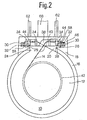
- the coil former 10 is provided with a winding 12 of a conductor 14, which is shown only schematically in FIG.
- a switching part (not shown) is guided in the form of a so-called pole tube in the coil former 10. When the switching device is actuated, the switching part can be used to control valves and thus determine their switching position.
- the bobbin 10 is almost flush with an essentially cylindrical housing part 16 made of metallic material.
- a holding device 18 is also formed from plastic material on one side of the coil former 10.
- the holding device 18 passes through an end recess 20 in the housing part 16 and is laterally in contact with the latter via a central piece 24, as is shown in particular in FIG.
- a flat plate 26 is arranged upwards on the middle piece 24 and forms a T-shaped base body of the holding device 18 with the middle piece 24.
- the lateral protrusions 28 lie in the transition area with the center piece 24 on the outer circumference of the housing part 16 and thus form a twist protection for the coil former 10 relative to the housing part 16.
- the holding device 18 has two peg-like extensions 30 arranged on the end of the base plate 26, around which the ends 32 of the conductor 14 are wound in order to ensure a firm connection of the conductor 12 to the holding device 18.
- two pairs of webs 34 are provided on the top of the plate 26 in the outer area, each of which has a receptacle 36 with a V-shaped cross section (see FIG. 1), in which the conductor 14 can be inserted.
- a guide bevel 38 is provided in the middle between the two webs 34 of the holding device 18 arranged directly opposite one another, by means of which the Conductor 14 crossing in the addressed area and without being touched at this point is guided (see Fig. 2,3).
- the turn package 12 is created and the conductor 14 is led out of the coil body 10 in such a way that it crosses the inlet slot 40 and the guide slope 38 into the receptacles 36 of the pair of webs 34 shown on the left in FIG reached. Then it is wrapped around the still free pin 30 and any excess ends of the conductor 14 are cut off.
- the conductor 14 is now guided by means of the holding device 18 over a predeterminable distance between the respective pairs of webs 34 in such a way that it is freely accessible from all sides for direct contact with two contact parts 44 of a device plug 46, since it is accessible from the webs 34 kept clear and taut and is at a distance from all fixed parts of the switching device between the respective receptacles 36 of a pair of webs 34.
- the device plug 46 has on its lower end facing the housing part 16 a peg-like projection 48 which engages in a bore 50 of the housing part 16 for establishing a connection.
- a latching part 52 can be provided on the housing part 16 for fixing the device plug 46, which engages under the holding device 18 along the recess 20, which at this point (see FIG. 1) has an axial projection 54 provided for this purpose having.
- the housing of the connector 46 and the locking part 52 are preferably formed from a plastic material and in view of this, a snap connection between the locking part 52 and the holding device 18 is possible.
- the respective contact part 44 of the device plug 16 has a roof-like connecting piece 56, which can be placed on the conductor piece between the two web pairs 34 from above.
- the two free leg pieces 58 of each connecting piece 56 which comprise the conductor 14 within the holding device 18, can be pressed together via the device and then welded to one another, the thin-walled plastic insulation of the conductor 14 being melted off, so that a conductive connection between the respective contact part 44 and the associated conductor piece of the conductor 14 is present.
- the roof-like connecting pieces 56 are connected to the outside with a flat contact track 60, on which is arranged perpendicular to it and connected to it there is a connector lug 62 which extends over the top of the switching device, as shown in particular in FIGS.
- a further contact track 64 is provided which forms the ground connection and which projects upwards with its one free end 66 as well as the connector tabs 62 and is welded to the outer periphery of the housing part 16 with its other free end 68 (see .Fig.1).
- All contact tracks 60 and 64 can be cut out or punched out of a flat board body and are then cast around with the plastic material of the connector 46.
- a socket 70 with an internal thread can be inserted in the connector 46 at the location of the pin-like projection 48, which ensures that the entire device is later attached to fixed parts and / or that the connector lugs 62 and 66 can be securely connected.
- the guide bevel 38 can also have a guide channel 72, the conductor 14 being placed in the interior of the channel, so that at the crossing point 74, at which the other end of the conductor is laid over the conductor 14 guided in the channel , there can be no short circuit. It is also sufficient, however, to let the conductor 14 run on one of the front sides of a guide or support of any kind, in which it is ensured that the crossing conductor pieces cannot touch each other due to their axial projection over the plate 26.
- the holding device 18, whose pairs of webs 34 form guide forks for the conductor 14, can be designed with a small overall height, so that, provided that the contact parts 44 cover the conductor 14 from above or from the side of the connector 46 on one side thereof create smaller dimensions for the switching device can be reached than was the case with the previously known.
Landscapes
- Engineering & Computer Science (AREA)
- Power Engineering (AREA)
- Details Of Connecting Devices For Male And Female Coupling (AREA)
- Electromagnets (AREA)
Claims (5)
- Dispositif de commutation, en particulier pour l'actionnement de soupapes, avec un connecteur (46) et une armature de la bobine de champ (10) dans laquelle est conduit un élément de commutation et qui est muni d'un enroulement (12) d'un conducteur (14) dont les extrémités (32) sont reliées avec un dispositif de fixation (18) composé d'un matériau isolant qui conduit à la réalisation d'une connexion électriquement conductrice avec des éléments de contact (44) du connecteur (46) entre les extrémités (32) et l'enroulement (12) du conducteur (14) par l'intermédiaire d'un trajet prédéterminable qui est accessible librement au moins par un côté pour un contact direct et sans enroulement avec les éléments de contact (44), caractérisé en ce que le dispositif de fixation (18) présente deux barrettes (34) correspondant à chaque élément de contact (44) qui disposent chacune d'un logement (36) dans lequel le conducteur (14) est guidé et que l'élément de contact (44) respectif présente une pièce de jonction en forme de toit (56) qui entoure au moins partiellement le conducteur (14) guidé entre les barrettes (34).
- Dispositif de commutation selon la revendication 1, caractérisé en ce qu'il est prévu un biais de guidage (38) disposé au milieu entre deux barrettes (34) du dispositif de fixation (18), biais de guidage à l'aide duquel le conducteur (14) est guidé de façon à s'entrecroiser sans se toucher à cet endroit.
- Dispositif de commutation selon l'une quelconque des revendications 1 ou 2, caractérisé en ce que le dispositif de fixation (18) est relié d'un seul tenant avec l'armature de la bobine de champ (10) et qu'il est en matière plastique.
- Dispositif de commutation selon l'une quelconque des revendications 1 à 3, caractérisé en ce que le connecteur (46) présente une partie en saillie (48) et/ou une pièce d'arrêt (52) avec laquelle il s'engrène dans un creux (50) de la partie de boîtier (16) ou il s'enclenche dans le dispositif de fixation (18) qui entoure l'armature de la bobine de champ (10).
- Dispositif de commutation selon l'une quelconque des revendications 1 à 4, caractérisé en ce que le connecteur (46) présente une connexion à la masse (64) qui est reliée avec un autre élément de contact (68) directement avec la partie de boîtier (16).
Applications Claiming Priority (2)
| Application Number | Priority Date | Filing Date | Title |
|---|---|---|---|
| DE4237354A DE4237354A1 (de) | 1992-11-05 | 1992-11-05 | Schaltvorrichtung |
| DE4237354 | 1992-11-05 |
Publications (2)
| Publication Number | Publication Date |
|---|---|
| EP0596356A1 EP0596356A1 (fr) | 1994-05-11 |
| EP0596356B1 true EP0596356B1 (fr) | 1997-05-14 |
Family
ID=6472163
Family Applications (1)
| Application Number | Title | Priority Date | Filing Date |
|---|---|---|---|
| EP93117232A Expired - Lifetime EP0596356B1 (fr) | 1992-11-05 | 1993-10-25 | Dispositif de commutation |
Country Status (3)
| Country | Link |
|---|---|
| EP (1) | EP0596356B1 (fr) |
| DE (2) | DE4237354A1 (fr) |
| ES (1) | ES2101192T3 (fr) |
Cited By (1)
| Publication number | Priority date | Publication date | Assignee | Title |
|---|---|---|---|---|
| DE10216731B3 (de) * | 2002-04-16 | 2004-01-08 | Hydac Electronic Gmbh | Elektromagnetische Schaltvorrichtung |
Families Citing this family (1)
| Publication number | Priority date | Publication date | Assignee | Title |
|---|---|---|---|---|
| DE10029279A1 (de) | 2000-06-14 | 2001-12-20 | Bosch Gmbh Robert | Zweiteilige Magnetspule und Verfahren zu deren Herstellung |
Family Cites Families (7)
| Publication number | Priority date | Publication date | Assignee | Title |
|---|---|---|---|---|
| GB917200A (en) * | 1960-05-17 | 1963-01-30 | Cav Ltd | Improved bobbin for a solenoid |
| DE3026761A1 (de) * | 1980-07-15 | 1982-02-11 | bso Steuerungstechnik GmbH, 6603 Sulzbach | Vorrichtung zum verbinden zweier draehte einer spule eines schaltmagneten mit je einem stecker |
| DE8234556U1 (de) * | 1982-12-09 | 1984-02-16 | Diehl GmbH & Co, 8500 Nürnberg | Elektrische spule |
| DE3407758A1 (de) * | 1984-03-02 | 1985-09-12 | Standard Elektrik Lorenz Ag, 7000 Stuttgart | Automatengerechter spulenkoerper fuer elektrische geraete |
| DE3930587A1 (de) * | 1989-09-13 | 1991-03-28 | Bosch Gmbh Robert | Zuendspule |
| DE69008284T2 (de) * | 1989-09-22 | 1994-09-15 | Aisin Seiki | Elektromagnetische Spulenvorrichtung. |
| JPH03204486A (ja) * | 1989-12-29 | 1991-09-06 | Aisin Aw Co Ltd | 電磁弁のコイル装置 |
-
1992
- 1992-11-05 DE DE4237354A patent/DE4237354A1/de not_active Withdrawn
-
1993
- 1993-10-25 ES ES93117232T patent/ES2101192T3/es not_active Expired - Lifetime
- 1993-10-25 EP EP93117232A patent/EP0596356B1/fr not_active Expired - Lifetime
- 1993-10-25 DE DE59306444T patent/DE59306444D1/de not_active Expired - Fee Related
Cited By (1)
| Publication number | Priority date | Publication date | Assignee | Title |
|---|---|---|---|---|
| DE10216731B3 (de) * | 2002-04-16 | 2004-01-08 | Hydac Electronic Gmbh | Elektromagnetische Schaltvorrichtung |
Also Published As
| Publication number | Publication date |
|---|---|
| DE59306444D1 (de) | 1997-06-19 |
| DE4237354A1 (de) | 1994-05-11 |
| EP0596356A1 (fr) | 1994-05-11 |
| ES2101192T3 (es) | 1997-07-01 |
Similar Documents
| Publication | Publication Date | Title |
|---|---|---|
| EP1096606B1 (fr) | Borne de connexion | |
| EP1109269B1 (fr) | Organe de contact électrique et douille de lampe avec un tel organe | |
| DE19800099A1 (de) | Leitungsverbinder | |
| DE19632821C2 (de) | Verdrahtungsplatte für elektrische Verbindungen | |
| DE2735838C2 (de) | Elektrische Anschlußklemme und elektrisches Kabelverbindungsglied | |
| DE4310369C2 (de) | Kontaktsatz für einen Steckverbinder | |
| EP1774545B1 (fr) | Support destine a un composant electrique | |
| DE10132123A1 (de) | Transformator | |
| EP0051130A1 (fr) | Connexion à douille coaxiale enfichable | |
| EP0176607B1 (fr) | Dispositif de liaison électrique au bout d'un bobinage | |
| EP0596356B1 (fr) | Dispositif de commutation | |
| DE4222685C2 (de) | Steckkontaktelement | |
| EP1382047B1 (fr) | Dispositif a bobine magnetique | |
| DE19529893A1 (de) | Elektrischer Verbinder | |
| EP0568899B1 (fr) | Prise de câble multipolaire | |
| DE19811667A1 (de) | Steckverbinder | |
| DE3784023T2 (de) | Elektrischer steckverbinder, der eine kombination individueller adapter und steckerstift-elemente als kontaktglied enthaelt. | |
| EP0127849B1 (fr) | Relais | |
| DE3641153C2 (fr) | ||
| DE19507029C1 (de) | Induktiver Drehzahlfühler | |
| EP0179259A1 (fr) | Corps de bobine | |
| DE3446105A1 (de) | Vorrichtung zum verbinden eines anschlusskabels mit den enden von auf einem spulenkoerper aufgebrachten wicklungen | |
| DE9205977U1 (de) | Mehrpoliger Kabelsteckverbinder | |
| DE69903900T2 (de) | Verbinderbasis für Spulenvorrichtung | |
| DE2924906C2 (fr) |
Legal Events
| Date | Code | Title | Description |
|---|---|---|---|
| PUAI | Public reference made under article 153(3) epc to a published international application that has entered the european phase |
Free format text: ORIGINAL CODE: 0009012 |
|
| AK | Designated contracting states |
Kind code of ref document: A1 Designated state(s): DE ES FR GB IE IT MC PT |
|
| 17P | Request for examination filed |
Effective date: 19940616 |
|
| 17Q | First examination report despatched |
Effective date: 19960112 |
|
| GRAG | Despatch of communication of intention to grant |
Free format text: ORIGINAL CODE: EPIDOS AGRA |
|
| GRAH | Despatch of communication of intention to grant a patent |
Free format text: ORIGINAL CODE: EPIDOS IGRA |
|
| GRAH | Despatch of communication of intention to grant a patent |
Free format text: ORIGINAL CODE: EPIDOS IGRA |
|
| GRAA | (expected) grant |
Free format text: ORIGINAL CODE: 0009210 |
|
| AK | Designated contracting states |
Kind code of ref document: B1 Designated state(s): DE ES FR GB IE IT MC PT |
|
| ET | Fr: translation filed | ||
| ITF | It: translation for a ep patent filed | ||
| GBT | Gb: translation of ep patent filed (gb section 77(6)(a)/1977) |
Effective date: 19970515 |
|
| REF | Corresponds to: |
Ref document number: 59306444 Country of ref document: DE Date of ref document: 19970619 |
|
| REG | Reference to a national code |
Ref country code: ES Ref legal event code: FG2A Ref document number: 2101192 Country of ref document: ES Kind code of ref document: T3 |
|
| REG | Reference to a national code |
Ref country code: PT Ref legal event code: SC4A Free format text: AVAILABILITY OF NATIONAL TRANSLATION Effective date: 19970806 |
|
| PLBE | No opposition filed within time limit |
Free format text: ORIGINAL CODE: 0009261 |
|
| STAA | Information on the status of an ep patent application or granted ep patent |
Free format text: STATUS: NO OPPOSITION FILED WITHIN TIME LIMIT |
|
| 26N | No opposition filed | ||
| REG | Reference to a national code |
Ref country code: FR Ref legal event code: TP |
|
| REG | Reference to a national code |
Ref country code: GB Ref legal event code: 732E |
|
| REG | Reference to a national code |
Ref country code: PT Ref legal event code: PC4A Free format text: HYDAC ELECTRONIC GMBH DE Effective date: 19991124 |
|
| REG | Reference to a national code |
Ref country code: GB Ref legal event code: IF02 |
|
| PGFP | Annual fee paid to national office [announced via postgrant information from national office to epo] |
Ref country code: GB Payment date: 20020918 Year of fee payment: 10 |
|
| PGFP | Annual fee paid to national office [announced via postgrant information from national office to epo] |
Ref country code: PT Payment date: 20020919 Year of fee payment: 10 |
|
| PGFP | Annual fee paid to national office [announced via postgrant information from national office to epo] |
Ref country code: MC Payment date: 20020926 Year of fee payment: 10 |
|
| PGFP | Annual fee paid to national office [announced via postgrant information from national office to epo] |
Ref country code: ES Payment date: 20021004 Year of fee payment: 10 |
|
| PGFP | Annual fee paid to national office [announced via postgrant information from national office to epo] |
Ref country code: FR Payment date: 20021029 Year of fee payment: 10 |
|
| PG25 | Lapsed in a contracting state [announced via postgrant information from national office to epo] |
Ref country code: GB Free format text: LAPSE BECAUSE OF NON-PAYMENT OF DUE FEES Effective date: 20031025 |
|
| PG25 | Lapsed in a contracting state [announced via postgrant information from national office to epo] |
Ref country code: ES Free format text: LAPSE BECAUSE OF NON-PAYMENT OF DUE FEES Effective date: 20031027 |
|
| PG25 | Lapsed in a contracting state [announced via postgrant information from national office to epo] |
Ref country code: MC Free format text: LAPSE BECAUSE OF NON-PAYMENT OF DUE FEES Effective date: 20031031 |
|
| PG25 | Lapsed in a contracting state [announced via postgrant information from national office to epo] |
Ref country code: PT Free format text: LAPSE BECAUSE OF NON-PAYMENT OF DUE FEES Effective date: 20040430 |
|
| GBPC | Gb: european patent ceased through non-payment of renewal fee |
Effective date: 20031025 |
|
| PG25 | Lapsed in a contracting state [announced via postgrant information from national office to epo] |
Ref country code: FR Free format text: LAPSE BECAUSE OF NON-PAYMENT OF DUE FEES Effective date: 20040630 |
|
| REG | Reference to a national code |
Ref country code: FR Ref legal event code: ST Ref country code: PT Ref legal event code: MM4A Free format text: LAPSE DUE TO NON-PAYMENT OF FEES Effective date: 20040430 |
|
| REG | Reference to a national code |
Ref country code: ES Ref legal event code: FD2A Effective date: 20031027 |
|
| PGFP | Annual fee paid to national office [announced via postgrant information from national office to epo] |
Ref country code: IE Payment date: 20051013 Year of fee payment: 13 |
|
| PG25 | Lapsed in a contracting state [announced via postgrant information from national office to epo] |
Ref country code: IE Free format text: LAPSE BECAUSE OF NON-PAYMENT OF DUE FEES Effective date: 20061025 |
|
| PGFP | Annual fee paid to national office [announced via postgrant information from national office to epo] |
Ref country code: IT Payment date: 20061031 Year of fee payment: 14 |
|
| REG | Reference to a national code |
Ref country code: IE Ref legal event code: MM4A |
|
| PGFP | Annual fee paid to national office [announced via postgrant information from national office to epo] |
Ref country code: DE Payment date: 20081028 Year of fee payment: 16 |
|
| PG25 | Lapsed in a contracting state [announced via postgrant information from national office to epo] |
Ref country code: IT Free format text: LAPSE BECAUSE OF NON-PAYMENT OF DUE FEES Effective date: 20071025 |
|
| PG25 | Lapsed in a contracting state [announced via postgrant information from national office to epo] |
Ref country code: DE Free format text: LAPSE BECAUSE OF NON-PAYMENT OF DUE FEES Effective date: 20100501 |