EP0596463B1 - Wavelength switching light source - Google Patents
Wavelength switching light source Download PDFInfo
- Publication number
- EP0596463B1 EP0596463B1 EP93117798A EP93117798A EP0596463B1 EP 0596463 B1 EP0596463 B1 EP 0596463B1 EP 93117798 A EP93117798 A EP 93117798A EP 93117798 A EP93117798 A EP 93117798A EP 0596463 B1 EP0596463 B1 EP 0596463B1
- Authority
- EP
- European Patent Office
- Prior art keywords
- wavelength
- light source
- current
- control signal
- output
- Prior art date
- Legal status (The legal status is an assumption and is not a legal conclusion. Google has not performed a legal analysis and makes no representation as to the accuracy of the status listed.)
- Expired - Lifetime
Links
- 230000003287 optical effect Effects 0.000 claims description 38
- BJQHLKABXJIVAM-UHFFFAOYSA-N bis(2-ethylhexyl) phthalate Chemical compound CCCCC(CC)COC(=O)C1=CC=CC=C1C(=O)OCC(CC)CCCC BJQHLKABXJIVAM-UHFFFAOYSA-N 0.000 claims description 3
- 230000000737 periodic effect Effects 0.000 claims description 3
- 239000004065 semiconductor Substances 0.000 description 7
- 238000010586 diagram Methods 0.000 description 5
- 230000005540 biological transmission Effects 0.000 description 2
- 239000013307 optical fiber Substances 0.000 description 2
- 230000000630 rising effect Effects 0.000 description 2
- 230000001419 dependent effect Effects 0.000 description 1
- 238000001514 detection method Methods 0.000 description 1
- 238000002347 injection Methods 0.000 description 1
- 239000007924 injection Substances 0.000 description 1
- 230000010355 oscillation Effects 0.000 description 1
- 230000000087 stabilizing effect Effects 0.000 description 1
Images

Classifications
-
- H—ELECTRICITY
- H01—ELECTRIC ELEMENTS
- H01S—DEVICES USING THE PROCESS OF LIGHT AMPLIFICATION BY STIMULATED EMISSION OF RADIATION [LASER] TO AMPLIFY OR GENERATE LIGHT; DEVICES USING STIMULATED EMISSION OF ELECTROMAGNETIC RADIATION IN WAVE RANGES OTHER THAN OPTICAL
- H01S5/00—Semiconductor lasers
- H01S5/06—Arrangements for controlling the laser output parameters, e.g. by operating on the active medium
- H01S5/068—Stabilisation of laser output parameters
- H01S5/0683—Stabilisation of laser output parameters by monitoring the optical output parameters
- H01S5/0687—Stabilising the frequency of the laser
Definitions
- the present invention relates to a wavelength switching light source for use in optical communication systems and the like, and more particularly to a wavelength switching light source capable of high-speed switching of the wavelength of output light.
- optical communication system requiring high-speed switching of the wavelength of output light include, for instance, the optical packet transfer network described in "Wavelength-addressed optical network using an ATM cell-based access scheme" (by N. Shimosaka et al.), Conference on Optical Fiber Communication/International Conference on Integrated Optics and Optical Fiber Communication, Technical Digest Series, Volume 4 (1993), pp. 49-50.
- the wavelength of the light source should be switched and the altered wavelength should be stabilized within the guard time left between consecutive packets.
- the arrangement described in this literature uses a variable-wavelength light source consisting of two semiconductor lasers and an optical switch for selectively supplying the output light of one or the other of the two semiconductor lasers.
- variable-wavelength light source whereas the oscillation wavelength of a semiconductor laser varies with temperature fluctuations and accordingly these temperature fluctuations should be compensated for, the variable-wavelength light source described in this literature requires either a temperature compensation circuit for each semiconductor laser or a constant temperature device accommodating a plurality of semiconductor lasers, and entails the problem that the dimensions of the variable-wavelength light source would increase with the number of wavelengths used.
- the object of the present invention is to provide a variable-wavelength light source whose dimensions will hardly enlarge even if a wavelength range used increases.
- a wavelength switching light source for varying the wavelength of the output light in accordance with a wavelength designating signal and a wavelength switching signal, both supplied from outside, comprising:
- the preferred embodiment of the invention consists of a variable-wavelength light source 101; a light brancher 102 for branching the output light of the variable-wavelength light source into two beams, of which one is supplied externally as an output light; an optical resonator 103, to which the other of the outputs of the light brancher 102 is supplied, for supplying transmitted light; a temperature control device 104 for accommodating the optical resonator 103; an optical detector 105 for outputting a voltage indicating the power of the transmitted light; an operational amplifier 106 for outputting, as a first wavelength control current, a current which is proportional to the balance of the subtraction of the output of the optical detector from a fixed reference voltage; a wavelength control circuit 108 for outputting a second wavelength control current in accordance with a wavelength switching signal 100-1 and a wavelength designation signal 100-2, both supplied from outside; and an adder 107 for adding the first wavelength control current signal and the second wavelength
- the variable-wavelength light source 101 outputs oscillating light of a wavelength corresponding to the wavelength control current supplied from the adder 107.
- this variable-wavelength light source can be used, for example, a DFB semiconductor laser.
- a DFB semiconductor laser has such a property that its oscillating wavelength lengthens with an increase in injection current.
- the oscillating light from the variable-wavelength light source 101 is branched by the light brancher 102 into two beams, of which one is emitted outside as output light and the other is brought to incidence on the optical resonator 103.
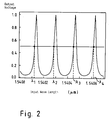
- the optical resonator 103 can be used a Fabri-Perot etalon, for instance, which shows a periodic wavelength transmission characteristic as shown in FIG. 2.
- the horizontal axis represents the wavelength of the input light and the vertical axis, the relative volume of the detection voltage at the time of detecting the transmitted light power with an optical detector.
- this optical resonator 103 can also be used a Mach-Zehnder type optical resonator.
- This optical resonator 103 is housed in the temperature control device 104 and kept at a constant temperature.
- the output voltage of the optical detector substantially varies in the rising and falling parts of the transmission characteristic. The intensity of this transmitted light is converted into a voltage by the optical detector 105.
- the output voltage of the optical detector 105 is supplied to the negative side input terminal of the operational amplifier 106.
- the positive side input terminal of the operational amplifier is supplied with a fixed reference voltage.
- This reference voltage is set at a level corresponding to the mid-point between the peak level and the bottom level of the input wavelength-optical detector output voltage characteristic shown in FIG. 2.
- wavelengths ⁇ 1, ⁇ 2, ⁇ 3, ⁇ 4,...., corresponding to the intersection points between this reference voltage and the rising parts of the wavelength-output voltage characteristic are the oscillating wavelengths at which the variable-wavelength light source 101 is to be set.
- the operational amplifier 106 supplies, as the first wavelength control current, a current of a value proportional to the balance of the subtraction of the optical detector output voltage from the reference voltage. This first wavelength control current is supplied to one of the input terminals of the adder 107.
- the oscillating wavelength of the variable-wavelength light source 101 is set at the wavelength ⁇ 2 in FIG. 2, when a current value i( ⁇ 2) to cause the variable wavelength light source 101 to oscillate at the wavelength ⁇ 2 is supplied, as the second wavelength control current, from the wavelength control circuit 108 to a second input terminal of the adder 107.
- the wavelength control circuit 108 outputs, as the second wavelength control current, a current of the value at which the variable-wavelength light source 101 oscillates at the wavelength ⁇ 2 when the first wavelength control current is made zero.
- the oscillating wavelength of the variable-wavelength light source 101 is lengthened by a temperature variation
- the output voltage of the optical detector will increase as is obvious from FIG. 2, and a negative current is supplied from the operational amplifier 106.
- the wavelength control current which is the output of the adder 107
- the output voltage of the optical detector 105 will decrease, the wavelength control current will increase, and the oscillating wavelength of the variable-wavelength light source 101 will lengthen. In this manner, the oscillating wavelength of the variable-wavelength light source 101 is stabilized at ⁇ 2.
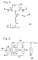
- the wavelength control circuit 108 will be described with reference to FIG. 3 as well.
- the wavelength control circuit 108 consists of two current sources 202 and 203, of which one supplies the second wavelength control current when the other is in a hot stand-by state, and a control circuit 201.
- the control circuit 201 in accordance with the wavelength switching signal 100-1 supplied from outside, switches via signal lines 206 and 207 the current source in the hot stand-by state to an active state and the other current source, which is in the active state, to the hot stand-by state.
- the control circuit 201 in accordance with the wavelength designation signal 100-2 supplied from outside, further supplies the current source in the hot stand-by state with a bias voltage required for oscillating the variable wavelength light source 101 at the designated wavelength.
- the current source 202 is in an active state and the current source 203, in a hot stand-by state. Then the current source 202 supplies the adder 107 with an already set constant current, for instance i( ⁇ 2) mentioned above. And when a wavelength designation signal indicating the wavelength ⁇ 2 is supplied via a signal line 100-2, the control circuit 201 supplies the current source 203 in the hot stand-by state via a signal line 205 with a bias voltage to cause the current i( ⁇ 2), which is required for having the variable-wavelength light source 101 oscillate at the wavelength ⁇ 2, corresponding to this wavelength designation signal, to be outputted. After that , when the wavelength switching signal 100-1 is supplied to the control circuit 201, the current source 202 shifts to the hot stand-by state, and the current source 203 takes on the active state to supply the current i( ⁇ 2) to the adder 107.
- a signal line 204 supplies a signal which shifts from a low to a high level, and this signal is supplied via a terminal A and a resistor R1 to the base terminal of a switching transistor Q1.
- the base terminal of another switching transistor Q2 is supplied via an inverter 401 and a resistor R2 with a signal which shifts from a high to a low level.
- the transistor Q1 is turned on, and the transistor Q2, turned off.
- the transistor Q1 is turned off and the transistor Q2, turned on.
- the output current of the current source 202 is not supplied to the adder 107 of FIG. 1 and, as stated already, a bias voltage corresponding to the wavelength to be used when this current source 202 takes on an active state next time is set at the base terminal of the transistor Q3 via the signal line 206.
- this preferred embodiment of the present invention requires no more than one optical resonator and one comparator for its temperature dependence stabilizing mechanism even if a large wavelength range is used, resulting in the advantage that the hardware dimensions will not enlarge.
- FIG. 5 illustrates a second conceivable configuration of the wavelength control circuit 108.
- a constant current source 204 which outputs a fixed current value all the time
- the output current values of current sources 202a and 203a of FIG. 5 are smaller than those of the current sources 202 and 203 of FIG. 3 by the output current value of the constant current source 204.
- wavelengths ⁇ 1, ⁇ 2, ⁇ 3, ⁇ 4, ... of FIG. 2 are to be used as the oscillating wavelengths of the variable-wavelength light source, the wavelength control circuit of FIG.
- the current value corresponding to the wavelength ⁇ 1 is supplied by the constant current source 204, and the current sources 202a and 203a need to supply nothing more than the current value corresponding to the difference between the desired wavelength and the wavelength ⁇ 1, so that this circuit consumes less power than that of FIG. 3.
Landscapes
- Physics & Mathematics (AREA)
- Condensed Matter Physics & Semiconductors (AREA)
- General Physics & Mathematics (AREA)
- Electromagnetism (AREA)
- Optics & Photonics (AREA)
- Semiconductor Lasers (AREA)
- Lasers (AREA)
Applications Claiming Priority (2)
| Application Number | Priority Date | Filing Date | Title |
|---|---|---|---|
| JP295036/92 | 1992-11-04 | ||
| JP4295036A JPH0783154B2 (ja) | 1992-11-04 | 1992-11-04 | 波長切り換え光源 |
Publications (2)
| Publication Number | Publication Date |
|---|---|
| EP0596463A1 EP0596463A1 (en) | 1994-05-11 |
| EP0596463B1 true EP0596463B1 (en) | 1996-02-07 |
Family
ID=17815494
Family Applications (1)
| Application Number | Title | Priority Date | Filing Date |
|---|---|---|---|
| EP93117798A Expired - Lifetime EP0596463B1 (en) | 1992-11-04 | 1993-11-03 | Wavelength switching light source |
Country Status (6)
| Country | Link |
|---|---|
| US (1) | US5394418A (ja) |
| EP (1) | EP0596463B1 (ja) |
| JP (1) | JPH0783154B2 (ja) |
| AU (1) | AU671490B2 (ja) |
| CA (1) | CA2102270C (ja) |
| DE (1) | DE69301523T2 (ja) |
Families Citing this family (7)
| Publication number | Priority date | Publication date | Assignee | Title |
|---|---|---|---|---|
| JPH07240558A (ja) * | 1994-02-28 | 1995-09-12 | Ando Electric Co Ltd | 波長可変半導体レーザ光源 |
| JPH07240716A (ja) * | 1994-02-28 | 1995-09-12 | Ando Electric Co Ltd | 可変波長光源 |
| FR2734953B1 (fr) * | 1995-05-29 | 1997-07-04 | France Telecom | Dispositif de commutation de frequences d'emission d'une source lumineuse |
| US5825792A (en) * | 1996-07-11 | 1998-10-20 | Northern Telecom Limited | Wavelength monitoring and control assembly for WDM optical transmission systems |
| JP3788232B2 (ja) | 2000-12-13 | 2006-06-21 | 日本電気株式会社 | 波長可変光送信器、その出力制御方法並及び光通信システム |
| DE102005028268B4 (de) * | 2005-06-14 | 2013-12-12 | Forschungsverbund Berlin E.V. | Verfahren und Vorrichtung zur Erzeugung und Detektion eines Raman-Spektrums |
| WO2008120375A1 (ja) * | 2007-03-29 | 2008-10-09 | Fujitsu Limited | 光伝送装置および光伝送方法 |
Family Cites Families (2)
| Publication number | Priority date | Publication date | Assignee | Title |
|---|---|---|---|---|
| JPS60117693A (ja) * | 1983-11-30 | 1985-06-25 | Fujitsu Ltd | 光周波数安定化装置 |
| JPS63143888A (ja) * | 1986-12-08 | 1988-06-16 | Yokogawa Electric Corp | レ−ザ発生装置の制御方法 |
-
1992
- 1992-11-04 JP JP4295036A patent/JPH0783154B2/ja not_active Expired - Lifetime
-
1993
- 1993-11-02 CA CA002102270A patent/CA2102270C/en not_active Expired - Lifetime
- 1993-11-03 EP EP93117798A patent/EP0596463B1/en not_active Expired - Lifetime
- 1993-11-03 DE DE69301523T patent/DE69301523T2/de not_active Expired - Lifetime
- 1993-11-03 AU AU50461/93A patent/AU671490B2/en not_active Expired
- 1993-11-04 US US08/147,643 patent/US5394418A/en not_active Expired - Lifetime
Also Published As
| Publication number | Publication date |
|---|---|
| CA2102270C (en) | 1999-04-06 |
| DE69301523T2 (de) | 1996-08-08 |
| US5394418A (en) | 1995-02-28 |
| DE69301523D1 (de) | 1996-03-21 |
| CA2102270A1 (en) | 1994-05-05 |
| EP0596463A1 (en) | 1994-05-11 |
| AU5046193A (en) | 1994-05-19 |
| AU671490B2 (en) | 1996-08-29 |
| JPH0783154B2 (ja) | 1995-09-06 |
| JPH06196785A (ja) | 1994-07-15 |
Similar Documents
| Publication | Publication Date | Title |
|---|---|---|
| US6058131A (en) | Wavelength stabilization of laser source using fiber Bragg grating feedback | |
| CA2119143C (en) | Wavelength stabilization | |
| US6891867B2 (en) | Control method and apparatus for stabilizing optical wavelength | |
| EP0671792B1 (en) | Laser control arrangement for tuning a laser | |
| US6229833B1 (en) | Laser diode protecting circuit and laser driving current control circuit | |
| GB2283126A (en) | A gain controllable optical amplifier | |
| US5394418A (en) | Wavelength switching light source | |
| EP0545534B1 (en) | Long term mode stabilization for distributed Bragg reflector laser | |
| US5861975A (en) | Wavelength stability circuit | |
| CA2164073C (en) | Transmission wavelength control method permitting efficient wavelength multiplexing, optical communication method, optical transmitter, optical transmitter-receiver apparatus, andoptical communication system | |
| EP0946006B1 (en) | Method and apparatus for controlling the optical power of an optical wavelength division multiplexed transmission signal | |
| US5285059A (en) | Method for controlling a tunable filter and an apparatus therefor | |
| EP0191780A1 (en) | High speed intensity modulated light source | |
| JP3167967B2 (ja) | 可変波長半導体レーザ装置 | |
| US5940198A (en) | Optical unit for synchronizing clock signals | |
| JPS62244185A (ja) | 半導体レ−ザ装置 | |
| KR100211583B1 (ko) | 파장 분할 다중방식 광전송 시스템을 위한 광원 안정화 시스템 | |
| EP0492480B1 (en) | A system for the generation of modulated optical signals | |
| JP2002319736A (ja) | レーザ光の波長調整装置 | |
| EP0483821B1 (en) | A method for controlling a tunable filter and an apparatus therefor | |
| KR100264542B1 (ko) | 더블유디엠 시스템에서 엘디 파장 초기화와 고정 시스템 | |
| KR100254744B1 (ko) | 더블유디엠 시스템에서 레이저 다이오드의 광파장 안정화 장치 | |
| Lugagne Delpon et al. | Operation of 4× 1 optical register as a fast access optical buffer memory | |
| WO2000022766A8 (en) | Wavelength stabilization in a transmitter of wdm system | |
| JP2025152510A (ja) | レーザ装置および制御方法 |
Legal Events
| Date | Code | Title | Description |
|---|---|---|---|
| PUAI | Public reference made under article 153(3) epc to a published international application that has entered the european phase |
Free format text: ORIGINAL CODE: 0009012 |
|
| 17P | Request for examination filed |
Effective date: 19940210 |
|
| AK | Designated contracting states |
Kind code of ref document: A1 Designated state(s): DE FR GB |
|
| 17Q | First examination report despatched |
Effective date: 19941213 |
|
| GRAA | (expected) grant |
Free format text: ORIGINAL CODE: 0009210 |
|
| AK | Designated contracting states |
Kind code of ref document: B1 Designated state(s): DE FR GB |
|
| REF | Corresponds to: |
Ref document number: 69301523 Country of ref document: DE Date of ref document: 19960321 |
|
| ET | Fr: translation filed | ||
| PLBE | No opposition filed within time limit |
Free format text: ORIGINAL CODE: 0009261 |
|
| STAA | Information on the status of an ep patent application or granted ep patent |
Free format text: STATUS: NO OPPOSITION FILED WITHIN TIME LIMIT |
|
| 26N | No opposition filed | ||
| REG | Reference to a national code |
Ref country code: GB Ref legal event code: IF02 |
|
| PGFP | Annual fee paid to national office [announced via postgrant information from national office to epo] |
Ref country code: FR Payment date: 20121130 Year of fee payment: 20 Ref country code: DE Payment date: 20121031 Year of fee payment: 20 |
|
| PGFP | Annual fee paid to national office [announced via postgrant information from national office to epo] |
Ref country code: GB Payment date: 20121031 Year of fee payment: 20 |
|
| REG | Reference to a national code |
Ref country code: DE Ref legal event code: R071 Ref document number: 69301523 Country of ref document: DE |
|
| REG | Reference to a national code |
Ref country code: GB Ref legal event code: PE20 Expiry date: 20131102 |
|
| PG25 | Lapsed in a contracting state [announced via postgrant information from national office to epo] |
Ref country code: DE Free format text: LAPSE BECAUSE OF EXPIRATION OF PROTECTION Effective date: 20131105 Ref country code: GB Free format text: LAPSE BECAUSE OF EXPIRATION OF PROTECTION Effective date: 20131102 |