EP0596593B1 - Procédé de gravure par plasma - Google Patents
Procédé de gravure par plasma Download PDFInfo
- Publication number
- EP0596593B1 EP0596593B1 EP93306236A EP93306236A EP0596593B1 EP 0596593 B1 EP0596593 B1 EP 0596593B1 EP 93306236 A EP93306236 A EP 93306236A EP 93306236 A EP93306236 A EP 93306236A EP 0596593 B1 EP0596593 B1 EP 0596593B1
- Authority
- EP
- European Patent Office
- Prior art keywords
- flow rate
- plasma
- sio
- tin
- etch
- Prior art date
- Legal status (The legal status is an assumption and is not a legal conclusion. Google has not performed a legal analysis and makes no representation as to the accuracy of the status listed.)
- Expired - Lifetime
Links
Images

Classifications
-
- H—ELECTRICITY
- H10—SEMICONDUCTOR DEVICES; ELECTRIC SOLID-STATE DEVICES NOT OTHERWISE PROVIDED FOR
- H10W—GENERIC PACKAGES, INTERCONNECTIONS, CONNECTORS OR OTHER CONSTRUCTIONAL DETAILS OF DEVICES COVERED BY CLASS H10
- H10W20/00—Interconnections in chips, wafers or substrates
- H10W20/01—Manufacture or treatment
- H10W20/071—Manufacture or treatment of dielectric parts thereof
- H10W20/081—Manufacture or treatment of dielectric parts thereof by forming openings in the dielectric parts
- H10W20/083—Manufacture or treatment of dielectric parts thereof by forming openings in the dielectric parts the openings being via holes penetrating underlying conductors
-
- H—ELECTRICITY
- H10—SEMICONDUCTOR DEVICES; ELECTRIC SOLID-STATE DEVICES NOT OTHERWISE PROVIDED FOR
- H10P—GENERIC PROCESSES OR APPARATUS FOR THE MANUFACTURE OR TREATMENT OF DEVICES COVERED BY CLASS H10
- H10P50/00—Etching of wafers, substrates or parts of devices
- H10P50/20—Dry etching; Plasma etching; Reactive-ion etching
- H10P50/28—Dry etching; Plasma etching; Reactive-ion etching of insulating materials
- H10P50/282—Dry etching; Plasma etching; Reactive-ion etching of insulating materials of inorganic materials
- H10P50/283—Dry etching; Plasma etching; Reactive-ion etching of insulating materials of inorganic materials by chemical means
-
- H—ELECTRICITY
- H10—SEMICONDUCTOR DEVICES; ELECTRIC SOLID-STATE DEVICES NOT OTHERWISE PROVIDED FOR
- H10P—GENERIC PROCESSES OR APPARATUS FOR THE MANUFACTURE OR TREATMENT OF DEVICES COVERED BY CLASS H10
- H10P72/00—Handling or holding of wafers, substrates or devices during manufacture or treatment thereof
- H10P72/04—Apparatus for manufacture or treatment
- H10P72/0402—Apparatus for fluid treatment
- H10P72/0418—Apparatus for fluid treatment for etching
- H10P72/0421—Apparatus for fluid treatment for etching for drying etching
-
- H—ELECTRICITY
- H10—SEMICONDUCTOR DEVICES; ELECTRIC SOLID-STATE DEVICES NOT OTHERWISE PROVIDED FOR
- H10W—GENERIC PACKAGES, INTERCONNECTIONS, CONNECTORS OR OTHER CONSTRUCTIONAL DETAILS OF DEVICES COVERED BY CLASS H10
- H10W20/00—Interconnections in chips, wafers or substrates
- H10W20/01—Manufacture or treatment
- H10W20/071—Manufacture or treatment of dielectric parts thereof
- H10W20/081—Manufacture or treatment of dielectric parts thereof by forming openings in the dielectric parts
Definitions
- the present invention relates to new dry etching processes for etching SiO x compounds or glass and in particular to a process which has applicability for making high aspect ratio holes in SiO x compounds or glass.
- Ion bombardment of surfaces is an important aspect of plasma etching, reactive ion etching, and sputter deposition. Ion bombardment also is an important part of several analytical techniques such as secondary ion mass spectrometry (SIMS) and low energy ion scattering spectroscopy (LEIS). Auger electron spectrometry (AES) also employs low energy inert gas ions for physical sputtering to obtain erosion to support depth profiling. Although these have become very important processes, the ion induced surface chemistry and alteration of new surface chemical, physical and electronic characteristics are very complex and remain poorly understood processes. This has lead to the empirical development of most commercial plasma assisted etching processes.
- SIMS secondary ion mass spectrometry
- LEIS low energy ion scattering spectroscopy
- AES Auger electron spectrometry
- Plasmas are partially ionized quasi-neutral gases. They can be created in a vacuum chamber by applying enough electric field to ionize the gases.
- the power source may be a DC electric field, inductive RF coil, microwaves or a capacitively coupled RF electric field. Electrons have small mass relative to other particles so most of the energy gained in these systems is initially absorbed by the electrons. These high energy electrons collide with other particles and ionize the gas and sustain the plasma. The typical ionization potential is high so that the majority of molecules and atoms stay neutral. Eventually, a DC potential will build up between a plasma and any dielectric surface nearby, preventing any further imbalance.
- semiconductor processing plasmas are in a state of thermal non-equilibrium and are affected by the following:
- Ion mixing is the process under which target atoms are relocated by ion impact, which process is broken up by recoil and cascade contributions. It is believed that mixing processes may be important in enhancing volatile product formation. This is distinct from sputtering in which near surface atoms receive enough momentum transfer perpendicular to the surface to overcome the surface potential barrier and thereby escape into the vacuum.
- Confined plasma reactors are one type of such apparatus which employ generally closely spaced parallel plates which are excited by an RF power source to induce and sustain the plasma therebetween.
- These relatively simple essentially parallel plate electrodes devices have the difficulty that the plasma density and ion energy cannot be separately controlled and accordingly high ion energies cannot be curtailed in high power requirement situations.
- these reactors consist of a pair of closely separated nearly planar electrodes characterized by pressure on the order of 39.9-66.6 Pa (0.3-0.5 Torr) operation for etch. This pressure generally gives them isotropic etch characteristics.
- these reactors have been too slow for commercial etch use in a single wafer operation.
- VIAS contact holes
- etching process is not limited to integrated circuits since there are many devices and objects made from SiO x , or glass which can be improved by an improved micromachinery process which can produce high aspect ratio holes in such materials.
- Interconnects are usually metal but can also be made from doped polysilicon. Several levels of interconnects separated by dielectric layers are usually required. Typically, the metal employed for the interconnects is Al or contains Al because it has low resistance and is relatively inexpensive to apply.
- DD-A-126082 discloses a method comprising the features of the precharacterizing portion of claim 1.
- the light mass cooling gas is preferably helium.
- etch process embodying the invention that can be used for making high aspect ratio holes in oxides of silicon, and/or glass. It has a high etch rate of SiO X and/or glass and a low etch rate of TiN.
- the etch process can also be used for making contact VIAS in a silicon integrated circuit where the deep VIAS and shallow VIAS can differ in depth by a factor of more than three without damage to the underlying region of the shallow VIA.
- N 2 as a process gas improves the discrimination of the process with respect to TiN etching.
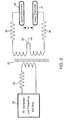
- the electric field to excite and maintain the plasma is provided by RF generator 30 at approximately 400 KHz.
- the RF transformer 31, having a grounded center tap 32 is coupled symmetrically to the upper and lower electrodes 20 and 21.
- Elements 33, 34, and 35 are for matching and tuning the cavity impedance to the RF generator.
- An inelastic collision is one in which there is no restriction on the type of energy interchanged and includes kinetic and internal or potential energy exchange.
- N 2 is reacting with the carbon and hydrogen so that more fluorine ion species were available for reacting with the SiO x .
Landscapes
- Drying Of Semiconductors (AREA)
- Internal Circuitry In Semiconductor Integrated Circuit Devices (AREA)
- ing And Chemical Polishing (AREA)
- Electrodes Of Semiconductors (AREA)
Claims (15)
- Procédé pour graver par plasma un matériau de SiOx à partir d'une plaquette, le procédé consistant àcaractérisé en ce que(a) établir un plasma dans un réacteur à plaques parallèles dans une zone confinée entre deux électrodes planes très proches l'une de l'autre en fournissant un flux de gaz réactifs à la zone confinée et une énergie RF à une fréquence d'environ 400 KHz à travers les électrodes; et(b) fixer la plaquette comportant ledit matériau de SiOx à graver à l'une des électrodes,(1) les gaz de réaction sont constitués de CHF3 et N2;(2) un débit élevé d'un gaz de faible masse est ajouté aux gaz de réaction pour augmenter la pression, de façon à refroidir le plasma par des collisions inélastiques accrues ; et(3) le flux des gaz est sélectionné en vue d'obtenir une pression de chambre totale, p., telle que 1333 Pa (10,0 Torr) > p > 199,95 Pa (1,5 Torr).
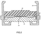
- Procédé selon la revendication 1 dans lequel l'électrode inférieure de ladite paire d'électrodes planes très proches l'une de l'autre présente une partie centrale bombée.
- Procédé selon la revendication 1 dans lequel le gaz de faible masse est l'He.
- Procédé selon la revendication 1, 2 ou 3, dans lequel la vitesse de gravure du SiOx est régulée en réglant le débit de gaz N2.
- Procédé selon la revendication 3 dans lequel la vitesse de gravure du SiOx est régulée en réglant le débit du gaz N2 dans la zone de 40 à 400 pour cent du débit de CHF3.
- Procédé selon l'une quelconque des revendications précédentes dans lequel le débit du gaz de faible masse est supérieur à, soit le débit de gaz N2, soit le débit de gaz CHF3.
- Procédé selon la revendication 6 dans lequel les débits de CHF3 et N2 sont du même ordre et le débit du gaz de refroidissement de faible masse est 50 à 100 fois supérieur , soit au débit du gaz CHF3, soit au débit du gaz N2.
- Procédé selon l'une quelconque des revendications précédentes dans lequel la plaquette à graver comprend également une couche de TiN formée au-dessous du matériau de SiOx avant la gravure, et dans lequel le matériau de SiOx est gravé sélectivement par le plasma à une vitesse supérieure à la vitesse de gravure de TiN par le plasma.
- Procédé selon la revendication 8 dans lequel le rapport de la vitesse de gravure du SiOx à celle du TiN se situe dans la zone de 20/1.
- Procédé selon l'une quelconque des revendications précédentes dans lequel les produits de gravure formés par la réaction de plasma avec le SiOx sont essentiellement entièrement volatiles pendant un temps suffisant pour permettre aux produits de gravure d'être éliminés dudit conteneur à vide avant une redéposition.
- Procédé selon la revendication 8 dans lequel le TiN est une couche d'arrêt telle que des trous peu profonds à paroi propre, présentant un rapport de dimensions élevé d'au moins 10, peuvent être gravés simultanément dans la plaquette comme des trous profonds, ces derniers étant trois fois plus profonds que les trous peu profonds.
- Procédé servant à produire des interconnexions métalliques entrecouches dans un circuit intégré supportant des bandes métalliques d'interconnexion, consistant à :(a) appliquer une couche de TiN sur le dessus des bandes d'interconnexion métalliques ;(b) appliquer une charge diélectrique de composés SiOx ou de verre sur les bandes métalliques d'interconnexion recouvertes de TiN;(c) aplanir le dessus de la charge diélectrique ;(d) appliquer et configurer un masque de résine photosensible sur le dessus de la couche aplanie pour fournir des VIAS en vue de connecter les fiches métalliques aux bandes d'interconnexion métalliques ;(e) placer la plaquette configurée dans un réacteur de gravure par plasma confiné et fixer la plaquette à une électrode du réacteur ;(f) introduire dans le réacteur à plaques parallèles des gaz de réaction constitués de CHF3 et N2 et ajouter un débit élevé d'un gaz de faible masse dans le réacteur pour augmenter la pression, de façon à refroidir le plasma par des collisions inélastiques accrues , le flux total étant réglé pour établir une pression de chambre totale p, telle que 1333Pa (10 Torr) > p > 199,95 Pa (1,5 Torr) ; et(g) exciter le plasma en appliquant une énergie RF à environ 400 KHz , de façon à graver les parties exposées de la charge diélectrique pour former des trous VIAS.
- Procédé selon la revendication 12 dans lequel le gaz de refroidissement de faible masse est l'He, et le débit d'He est supérieur au débit de l'un ou de l'autre de CHF3 et de N2.
- Procédé selon la revendication 13 dans lequel la couche de TiN présente une épaisseur dans la zone de 100 nanomètres (1000 Å).
- Procédé selon la revendication 14 comprenant une étape supplémentaire (h), l'étape (h) consistant à remplir les trous VIA avec une broche de Ti ou de Ti/TiN et de tungstène, la broche présentant une résistance dans la gamme de 1,2 ohm pour une broche de VIA d'un diamètre de 0,8 micromètre.
Applications Claiming Priority (2)
| Application Number | Priority Date | Filing Date | Title |
|---|---|---|---|
| US960499 | 1978-11-13 | ||
| US07/960,499 US5468339A (en) | 1992-10-09 | 1992-10-09 | Plasma etch process |
Publications (2)
| Publication Number | Publication Date |
|---|---|
| EP0596593A1 EP0596593A1 (fr) | 1994-05-11 |
| EP0596593B1 true EP0596593B1 (fr) | 1998-11-11 |
Family
ID=25503250
Family Applications (1)
| Application Number | Title | Priority Date | Filing Date |
|---|---|---|---|
| EP93306236A Expired - Lifetime EP0596593B1 (fr) | 1992-10-09 | 1993-08-06 | Procédé de gravure par plasma |
Country Status (6)
| Country | Link |
|---|---|
| US (1) | US5468339A (fr) |
| EP (1) | EP0596593B1 (fr) |
| JP (1) | JP3339920B2 (fr) |
| KR (1) | KR940010217A (fr) |
| DE (1) | DE69322058T2 (fr) |
| TW (1) | TW214606B (fr) |
Families Citing this family (19)
| Publication number | Priority date | Publication date | Assignee | Title |
|---|---|---|---|---|
| US5468340A (en) * | 1992-10-09 | 1995-11-21 | Gupta; Subhash | Highly selective high aspect ratio oxide etch method and products made by the process |
| US5935877A (en) * | 1995-09-01 | 1999-08-10 | Applied Materials, Inc. | Etch process for forming contacts over titanium silicide |
| US5843846A (en) * | 1996-12-31 | 1998-12-01 | Intel Corporation | Etch process to produce rounded top corners for sub-micron silicon trench applications |
| US5882535A (en) * | 1997-02-04 | 1999-03-16 | Micron Technology, Inc. | Method for forming a hole in a semiconductor device |
| US5961791A (en) * | 1997-02-26 | 1999-10-05 | Motorola, Inc. | Process for fabricating a semiconductor device |
| US5893752A (en) * | 1997-12-22 | 1999-04-13 | Motorola, Inc. | Process for forming a semiconductor device |
| US6090304A (en) * | 1997-08-28 | 2000-07-18 | Lam Research Corporation | Methods for selective plasma etch |
| US6183655B1 (en) | 1997-09-19 | 2001-02-06 | Applied Materials, Inc. | Tunable process for selectively etching oxide using fluoropropylene and a hydrofluorocarbon |
| US6066566A (en) * | 1998-01-28 | 2000-05-23 | International Business Machines Corporation | High selectivity collar oxide etch processes |
| US6080676A (en) * | 1998-09-17 | 2000-06-27 | Advanced Micro Devices, Inc. | Device and method for etching spacers formed upon an integrated circuit gate conductor |
| US6281132B1 (en) | 1998-10-06 | 2001-08-28 | Advanced Micro Devices, Inc. | Device and method for etching nitride spacers formed upon an integrated circuit gate conductor |
| US6214742B1 (en) * | 1998-12-07 | 2001-04-10 | Advanced Micro Devices, Inc. | Post-via tin removal for via resistance improvement |
| US6169036B1 (en) | 1999-03-25 | 2001-01-02 | Lucent Technologies Inc. | Method for cleaning via openings in integrated circuit manufacturing |
| DE10027932C2 (de) * | 2000-05-31 | 2003-10-02 | Infineon Technologies Ag | Verfahren zur Bildung eines Kontaktlochs in einer Isolierschicht eines elektronischen oder mikroelektronischen Bauelements |
| US6569774B1 (en) | 2000-08-31 | 2003-05-27 | Micron Technology, Inc. | Method to eliminate striations and surface roughness caused by dry etch |
| US6630407B2 (en) * | 2001-03-30 | 2003-10-07 | Lam Research Corporation | Plasma etching of organic antireflective coating |
| JP4176365B2 (ja) * | 2002-03-25 | 2008-11-05 | 東京エレクトロン株式会社 | プラズマエッチング方法 |
| US7608195B2 (en) | 2006-02-21 | 2009-10-27 | Micron Technology, Inc. | High aspect ratio contacts |
| US7648872B2 (en) | 2006-12-11 | 2010-01-19 | Micron Technology, Inc. | Methods of forming DRAM arrays |
Citations (1)
| Publication number | Priority date | Publication date | Assignee | Title |
|---|---|---|---|---|
| US5468340A (en) * | 1992-10-09 | 1995-11-21 | Gupta; Subhash | Highly selective high aspect ratio oxide etch method and products made by the process |
Family Cites Families (13)
| Publication number | Priority date | Publication date | Assignee | Title |
|---|---|---|---|---|
| US4028155A (en) * | 1974-02-28 | 1977-06-07 | Lfe Corporation | Process and material for manufacturing thin film integrated circuits |
| JPS5813625B2 (ja) * | 1979-12-12 | 1983-03-15 | 超エル・エス・アイ技術研究組合 | ガスプラズマ食刻法 |
| US4534816A (en) * | 1984-06-22 | 1985-08-13 | International Business Machines Corporation | Single wafer plasma etch reactor |
| US5227335A (en) * | 1986-11-10 | 1993-07-13 | At&T Bell Laboratories | Tungsten metallization |
| GB2214709A (en) * | 1988-01-20 | 1989-09-06 | Philips Nv | A method of enabling connection to a substructure forming part of an electronic device |
| DD288481A5 (de) * | 1989-10-12 | 1991-03-28 | Veb Mikroelektronik "Anna Seghers" Neuhaus,De | Verfahren zur plasmachemischen erzeugung von sio tief 2-strukturen fuer die herstellung von elektronischen bauelementen |
| US5254213A (en) * | 1989-10-25 | 1993-10-19 | Matsushita Electric Industrial Co., Ltd. | Method of forming contact windows |
| US4978420A (en) * | 1990-01-03 | 1990-12-18 | Hewlett-Packard Company | Single chamber via etch through a dual-layer dielectric |
| US5021121A (en) * | 1990-02-16 | 1991-06-04 | Applied Materials, Inc. | Process for RIE etching silicon dioxide |
| US5213659A (en) * | 1990-06-20 | 1993-05-25 | Micron Technology, Inc. | Combination usage of noble gases for dry etching semiconductor wafers |
| US5176790A (en) * | 1991-09-25 | 1993-01-05 | Applied Materials, Inc. | Process for forming a via in an integrated circuit structure by etching through an insulation layer while inhibiting sputtering of underlying metal |
| US5269879A (en) * | 1991-10-16 | 1993-12-14 | Lam Research Corporation | Method of etching vias without sputtering of underlying electrically conductive layer |
| US5284549A (en) * | 1992-01-02 | 1994-02-08 | International Business Machines Corporation | Selective fluorocarbon-based RIE process utilizing a nitrogen additive |
-
1992
- 1992-10-09 US US07/960,499 patent/US5468339A/en not_active Expired - Fee Related
-
1993
- 1993-05-12 TW TW082103707A patent/TW214606B/zh active
- 1993-06-03 KR KR1019930009997A patent/KR940010217A/ko not_active Abandoned
- 1993-06-21 JP JP14924293A patent/JP3339920B2/ja not_active Expired - Lifetime
- 1993-08-06 EP EP93306236A patent/EP0596593B1/fr not_active Expired - Lifetime
- 1993-08-06 DE DE69322058T patent/DE69322058T2/de not_active Expired - Lifetime
Patent Citations (1)
| Publication number | Priority date | Publication date | Assignee | Title |
|---|---|---|---|---|
| US5468340A (en) * | 1992-10-09 | 1995-11-21 | Gupta; Subhash | Highly selective high aspect ratio oxide etch method and products made by the process |
Also Published As
| Publication number | Publication date |
|---|---|
| DE69322058T2 (de) | 1999-07-01 |
| JP3339920B2 (ja) | 2002-10-28 |
| KR940010217A (ko) | 1994-05-24 |
| EP0596593A1 (fr) | 1994-05-11 |
| US5468339A (en) | 1995-11-21 |
| DE69322058D1 (de) | 1998-12-17 |
| TW214606B (en) | 1993-10-11 |
| JPH06151385A (ja) | 1994-05-31 |
Similar Documents
| Publication | Publication Date | Title |
|---|---|---|
| US5468339A (en) | Plasma etch process | |
| EP1047122B1 (fr) | Procédé de gravure anisotrope de substrats | |
| KR101083623B1 (ko) | 가스 화학물질의 주기적 조절을 사용하는 플라즈마 에칭방법 | |
| KR960000375B1 (ko) | 반도체장치의 제조방법 | |
| US6090717A (en) | High density plasma etching of metallization layer using chlorine and nitrogen | |
| US6284149B1 (en) | High-density plasma etching of carbon-based low-k materials in a integrated circuit | |
| US5772906A (en) | Mechanism for uniform etching by minimizing effects of etch rate loading | |
| EP0814500B1 (fr) | Procédé de gravure des structures polyciure | |
| US20040072443A1 (en) | Method for plasma etching performance enhancement | |
| JPH05308062A (ja) | ドライエッチング方法 | |
| US5880033A (en) | Method for etching metal silicide with high selectivity to polysilicon | |
| EP1374288A2 (fr) | Procede de gravure au plasma d'un revetement organique antireflechissant | |
| KR100535961B1 (ko) | 플라즈마에 의해 유도되는 차징 결함을 감소시키는 방법 | |
| JP2988455B2 (ja) | プラズマエッチング方法 | |
| US6410451B2 (en) | Techniques for improving etching in a plasma processing chamber | |
| EP1010203B1 (fr) | Procede d'attaque chimique d'une couche conductrice | |
| JP3464061B2 (ja) | SiOX層をその上に有する基板中にアスペクト比の高いホールまたは開口部をプラズマエッチングするための方法 | |
| US6228774B1 (en) | High aspect ratio sub-micron contact etch process in an inductively-coupled plasma processing system | |
| US5908320A (en) | High selectivity BPSG:TiSi2 contact etch process | |
| JPH04137532A (ja) | 表面処理方法及びその装置 | |
| JPH0461333A (ja) | 表面処理方法 | |
| JPH0590217A (ja) | ドライエツチング方法 | |
| JPH0770510B2 (ja) | プラズマ処理装置 | |
| JPH088244B2 (ja) | ドライエッチング方法 | |
| JPH0637058A (ja) | ドライエッチング方法 |
Legal Events
| Date | Code | Title | Description |
|---|---|---|---|
| PUAI | Public reference made under article 153(3) epc to a published international application that has entered the european phase |
Free format text: ORIGINAL CODE: 0009012 |
|
| AK | Designated contracting states |
Kind code of ref document: A1 Designated state(s): BE DE DK ES FR GB GR IE IT LU NL PT |
|
| 17P | Request for examination filed |
Effective date: 19941012 |
|
| 17Q | First examination report despatched |
Effective date: 19950403 |
|
| GRAG | Despatch of communication of intention to grant |
Free format text: ORIGINAL CODE: EPIDOS AGRA |
|
| GRAG | Despatch of communication of intention to grant |
Free format text: ORIGINAL CODE: EPIDOS AGRA |
|
| GRAH | Despatch of communication of intention to grant a patent |
Free format text: ORIGINAL CODE: EPIDOS IGRA |
|
| GRAH | Despatch of communication of intention to grant a patent |
Free format text: ORIGINAL CODE: EPIDOS IGRA |
|
| GRAA | (expected) grant |
Free format text: ORIGINAL CODE: 0009210 |
|
| AK | Designated contracting states |
Kind code of ref document: B1 Designated state(s): BE DE DK ES FR GB GR IE IT LU NL PT |
|
| PG25 | Lapsed in a contracting state [announced via postgrant information from national office to epo] |
Ref country code: GR Free format text: LAPSE BECAUSE OF NON-PAYMENT OF DUE FEES Effective date: 19981111 Ref country code: ES Free format text: THE PATENT HAS BEEN ANNULLED BY A DECISION OF A NATIONAL AUTHORITY Effective date: 19981111 Ref country code: BE Free format text: LAPSE BECAUSE OF FAILURE TO SUBMIT A TRANSLATION OF THE DESCRIPTION OR TO PAY THE FEE WITHIN THE PRESCRIBED TIME-LIMIT Effective date: 19981111 |
|
| REF | Corresponds to: |
Ref document number: 69322058 Country of ref document: DE Date of ref document: 19981217 |
|
| ET | Fr: translation filed | ||
| REG | Reference to a national code |
Ref country code: IE Ref legal event code: FG4D |
|
| ITF | It: translation for a ep patent filed | ||
| PG25 | Lapsed in a contracting state [announced via postgrant information from national office to epo] |
Ref country code: PT Free format text: LAPSE BECAUSE OF FAILURE TO SUBMIT A TRANSLATION OF THE DESCRIPTION OR TO PAY THE FEE WITHIN THE PRESCRIBED TIME-LIMIT Effective date: 19990211 Ref country code: DK Free format text: LAPSE BECAUSE OF FAILURE TO SUBMIT A TRANSLATION OF THE DESCRIPTION OR TO PAY THE FEE WITHIN THE PRESCRIBED TIME-LIMIT Effective date: 19990211 |
|
| PG25 | Lapsed in a contracting state [announced via postgrant information from national office to epo] |
Ref country code: LU Free format text: LAPSE BECAUSE OF NON-PAYMENT OF DUE FEES Effective date: 19990806 |
|
| PLBE | No opposition filed within time limit |
Free format text: ORIGINAL CODE: 0009261 |
|
| STAA | Information on the status of an ep patent application or granted ep patent |
Free format text: STATUS: NO OPPOSITION FILED WITHIN TIME LIMIT |
|
| 26N | No opposition filed | ||
| REG | Reference to a national code |
Ref country code: GB Ref legal event code: IF02 |
|
| PGFP | Annual fee paid to national office [announced via postgrant information from national office to epo] |
Ref country code: NL Payment date: 20020618 Year of fee payment: 10 |
|
| PGFP | Annual fee paid to national office [announced via postgrant information from national office to epo] |
Ref country code: IE Payment date: 20020722 Year of fee payment: 10 |
|
| PG25 | Lapsed in a contracting state [announced via postgrant information from national office to epo] |
Ref country code: IE Free format text: LAPSE BECAUSE OF NON-PAYMENT OF DUE FEES Effective date: 20030806 |
|
| PG25 | Lapsed in a contracting state [announced via postgrant information from national office to epo] |
Ref country code: NL Free format text: LAPSE BECAUSE OF NON-PAYMENT OF DUE FEES Effective date: 20040301 |
|
| NLV4 | Nl: lapsed or anulled due to non-payment of the annual fee |
Effective date: 20040301 |
|
| REG | Reference to a national code |
Ref country code: IE Ref legal event code: MM4A |
|
| PG25 | Lapsed in a contracting state [announced via postgrant information from national office to epo] |
Ref country code: IT Free format text: LAPSE BECAUSE OF NON-PAYMENT OF DUE FEES Effective date: 20050806 |
|
| PGFP | Annual fee paid to national office [announced via postgrant information from national office to epo] |
Ref country code: GB Payment date: 20120726 Year of fee payment: 20 |
|
| PGFP | Annual fee paid to national office [announced via postgrant information from national office to epo] |
Ref country code: FR Payment date: 20120809 Year of fee payment: 20 Ref country code: DE Payment date: 20120831 Year of fee payment: 20 |
|
| REG | Reference to a national code |
Ref country code: DE Ref legal event code: R071 Ref document number: 69322058 Country of ref document: DE |
|
| REG | Reference to a national code |
Ref country code: GB Ref legal event code: PE20 Expiry date: 20130805 |
|
| PG25 | Lapsed in a contracting state [announced via postgrant information from national office to epo] |
Ref country code: DE Free format text: LAPSE BECAUSE OF EXPIRATION OF PROTECTION Effective date: 20130807 |
|
| PG25 | Lapsed in a contracting state [announced via postgrant information from national office to epo] |
Ref country code: GB Free format text: LAPSE BECAUSE OF EXPIRATION OF PROTECTION Effective date: 20130805 |