EP0596636A2 - Cache-Etikettenspeicher - Google Patents
Cache-Etikettenspeicher Download PDFInfo
- Publication number
- EP0596636A2 EP0596636A2 EP93308502A EP93308502A EP0596636A2 EP 0596636 A2 EP0596636 A2 EP 0596636A2 EP 93308502 A EP93308502 A EP 93308502A EP 93308502 A EP93308502 A EP 93308502A EP 0596636 A2 EP0596636 A2 EP 0596636A2
- Authority
- EP
- European Patent Office
- Prior art keywords
- memory
- port
- memory array
- cache
- cache tag
- Prior art date
- Legal status (The legal status is an assumption and is not a legal conclusion. Google has not performed a legal analysis and makes no representation as to the accuracy of the status listed.)
- Granted
Links
Images
Classifications
-
- G—PHYSICS
- G06—COMPUTING OR CALCULATING; COUNTING
- G06F—ELECTRIC DIGITAL DATA PROCESSING
- G06F12/00—Accessing, addressing or allocating within memory systems or architectures
- G06F12/02—Addressing or allocation; Relocation
- G06F12/08—Addressing or allocation; Relocation in hierarchically structured memory systems, e.g. virtual memory systems
- G06F12/0802—Addressing of a memory level in which the access to the desired data or data block requires associative addressing means, e.g. caches
- G06F12/0806—Multiuser, multiprocessor or multiprocessing cache systems
- G06F12/0815—Cache consistency protocols
- G06F12/0831—Cache consistency protocols using a bus scheme, e.g. with bus monitoring or watching means
-
- G—PHYSICS
- G06—COMPUTING OR CALCULATING; COUNTING
- G06F—ELECTRIC DIGITAL DATA PROCESSING
- G06F12/00—Accessing, addressing or allocating within memory systems or architectures
- G06F12/02—Addressing or allocation; Relocation
- G06F12/08—Addressing or allocation; Relocation in hierarchically structured memory systems, e.g. virtual memory systems
- G06F12/0802—Addressing of a memory level in which the access to the desired data or data block requires associative addressing means, e.g. caches
- G06F12/0844—Multiple simultaneous or quasi-simultaneous cache accessing
- G06F12/0853—Cache with multiport tag or data arrays
Definitions
- the present invention relates in general to digital computer systems, and more particularly to cache memory systems.
- Cache memories are used in many computer systems to improve system performance.
- a cache memory is a relatively small, fast memory which resides between a central processor and main system memory. Whenever the processor reads the contents of a memory location which is stored in the cache memory, the time required to access such location is drastically reduced.
- a good cache technique can provide a "hit ratio" of well over ninety percent, meaning that no main memory access is necessary for over ninety percent of the read operations performed. Access of data which is stored in the cache can improve access times by factors of three to ten times.
- a cache performs functions requiring two different types of memory.
- the first type is the data memory, in which the data is actually stored.
- the second type is known as a tag memory, or tag RAM, which is used to determine which memory locations are actually stored in the cache.
- the cache tag RAM contains a plurality of entries corresponding to the entries of the data cache. Each entry is indexed by some number of least significant bits of the address generated by the central processor, with the tag entry itself containing the most significant bits of the memory location which is stored in the corresponding data cache entry.
- each processor in a system with its own cache memory.
- Each local processor accesses its own cache whenever possible, and accesses main system memory through a system bus only when necessary.
- cache coherency problem This problem arises whenever it is possible for shared variables in main system memory to be accessed by two or more processors in the system. These processors can be local central processing units, or input/output devices attached to the bus.
- the cache coherency problem arises when a single memory location is cached in two or more local caches. If one of the processors writes a new value into that memory location, it will be inconsistent with the value of the same variable, or main memory location, currently cached in the other caches.
- the cache coherency problem also arises when a non-caching device writes to a location in system memory which has been cached by another device.
- One technique utilized in dealing with the cache coherency problem is to have all local processors having caches monitor, or "snoop," the main system bus at all times. If another processor or device writes data to a memory location which is currently stored in a local cache, the local cache entry is invalidated. If that location is later accessed by the local processor, the updated data is then retrieved from the main system memory.
- Using a dual-port memory array in this manner results in an area penalty on the tag RAM chip. This is because a dual-port memory, compared to a single-port memory array, can be two and a half to three and a half times larger, or more.
- a cache tag memory device which has a memory array comprising a first single-port memory array, a second single-port memory array, and a dual-port memory array.
- a first port accessed by a local processor, may read from and write to its corresponding single-port memory array and the dual-port memory array.
- a second port accessed through a global system bus, may also read from and write to its corresponding second single-port memory array and the dual-port memory array Both ports operate asynchronously relative to each other.
- Status bits indicating the status of the entries in the first and second single-port memory arrays are stored in the dual-port memory array and may be altered by the global system while the local processor is performing its operations.
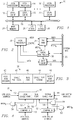
- a multi-processor computer system is illustrated and referred to generally with the reference number 10 .
- Local processors 12, 14, 16 are each provided with a local cache memory 18, 20, 22 .
- the processors 12, 14, 16 communicate with each other and with a main system memory 24 through a system bus 26 .
- a plurality of input/output devices 28, 30 are also attached to the system bus 26 . Input/output devices 28, 30 typically do not contain local cache memories.
- local cache memories 18 and 20 may each contain a copy of a shared variable from main system memory 24. If local processor 14 updates the value of the shared variable, local cache 20 will be updated as will main system memory 24 .
- a technique as disclosed in United States Patent Application Serial No. 07/473239, entitled DUAL-PORT CACHE TAG MEMORY, filed on January 31, 1990, which is incorporated herein by reference, is utilized to ensure that the outdated value for such local variable stored in cache memory 18 is marked as invalid.
- input/output device 28 writes a value to main memory 24 . If such memory location has previously been cached in local cache memory 18 , the current memory data and the data in local cache memory 18 will not be the same.
- FIG. 2 a high level block diagram showing a cache memory utilizing a cache tag memory according to the present invention is depicted.
- a preferred system for ensuring cache coherency in a single or multi-processor system will also be described.
- a data cache 32 and cache tag RAM 34 communicate with system bus 26 and local processor 36 .
- Cache controller 38 performs the usual cache control functions found in caches which are suitable for use with single processor systems.
- Data cache 32 exchanges data with the local processor 36 and system bus 26 under control of cache controller 38 .
- Various control signals are exchanged by the local processor 36 and cache controller 38 , and between cache controller 38 and system bus 26 .
- Address and control signals are communicated from local processor 36 to cache tag RAM 34.
- Address and control signals are also communicated between cache tag RAM 34 and system bus 26.
- a control signal SW is communicated to cache tag RAM 34 from system bus 26 to indicate that a write operation, referred to as a snoop write, is occurring on the system bus 26 .
- a control signal MTCH B is returned to system bus 26 whenever a system bus address matches an entry in cache tag RAM 34 during a snoop write operation.
- the signal MTCHB can be used as desired by the system in performance of cache control functions.
- Cache tag RAM 34 also passes a signal MTCH A to cache controller 38 .
- MTCH A indicates that the memory location currently being addressed by local processor 36 resides in the data cache 32 , and that the entry is currently valid.
- Cache controller 38 then causes the location being accessed by local processor 36 to be read directly from data cache 32 . If MTCH A indicates a miss, cache controller 38 causes the contents of the address location to be accessed from main memory over system bus 26 .
- FIG. 3 is a block diagram of a preferred cache tag memory, referred to generally by the reference number 34.
- Cache tag memory 34 includes a first single-port memory array 40 with a corresponding row decoder 42.
- the first single-port memory array 40 is dedicated to a local processor.
- a second single-port memory array 44 and corresponding row decoder 46 is preferably dedicated to the system or main memory.
- a dual-port memory array 48 is utilized to store information or status bits about the cache memory.
- the status bits stored in the dual-port memory array 48 are shared by both the first and second single-port memory arrays 40, 44. Examples of status bits include a snoop valid bit, parity bit, or bits required for MOESI protocol.
- MOESI stands for Modified, Owned, Exclusive, Shared, and Invalid, and is utilized to -indicate cache states. Essentially, any bit which may be altered by the system port while the local processor is performing its operations is stored in the dual-port memory array 48 .
- the size difference between a dual-port memory array and a single-port memory array can be two and a half to three and a half times larger, or more.
- having a cache tag memory which has two single-port memory arrays and a small dual-port memory array results in space savings on the chip.
- the area difference between an all dual-port cache tag memory and the preferred cache tag memory is calculated below for a cache tag memory which utilizes a tag which is 16 bits wide plus 2 status bits (total 18 bits wide).
- all dual-port 18 bits x R preferred cache tag: (2 bits x R) + (16 bits x 2)
- the ratio of the size of a dual-port to the size of a single-port memory array is denoted by the variable R.
- the cache tag RAM 34 includes a first single-port memory array 40 dedicated to the local processor, a second single-port memory array 44 dedicated to the system or main memory, and a dual-port memory array 48 .
- the dual-port memory array 48 stores information or status bits about the cache memory, and its entries are shared by the two single-port memory arrays 40, 44.
- First single-port memory array 40 is addressed by the least significant bits (LSB) of the address from the local processor.
- the most significant bits (MSB) of the local address are input to a comparator 50 where they are compared with the first single-port memory array 40 entry currently selected by the local address LSB, which is available on line 52 .
- a logical one is output from comparator 50 if the selected entry matches the MSB of the local address, and is connected to one input of AND gate 54.
- the snoop valid bit 56 from the corresponding address is also connected as an input to AND gate 54, and the output of AND gate 54 defines the signal MTCH A .
- signal MTCH A is a logical one, indicating a cache hit, only if the first single-port memory array 40 entry indexed by the LSB of the local address matches the MSB of the local address, and the corresponding snoop valid bit 56 for that entry is a logical one.
- Second single-port memory array 44 is addressed by the LSB of the system address.
- the entry corresponding to such location within the array is output on data line 58 and connected to comparator 60 .
- Comparator 60 compares the entry present on line 58 with the MSB of the system address, generating a logical one if they match.
- the output of comparator 60 is connected to an input of both AND gates 62, 64.
- the snoop valid bit 56 of the entry indexed by the LSB of the system address is also connected to AND gate 62 .
- the signal MTCH B is a logical one only if the selected entry matches the MSB of the system address, and the snoop valid bit 56 has a value of logical one.
- a snoop write signal (SW) connected to a second input of AND gate 64.
- the output of AND gate 64 will be a logical one only if the address MSB on the system bus matches the entry in the second single-port memory array 44 indexed by the system address LSB, and a write operation is being performed on the system bus. In such event, the value stored in the data cache for such entry is now out of date, and must be marked as invalid.
- the output of AND gate 64 is a logical one, the snoop valid bit of the entry indexed by the LSB of the current system address is reset to a logical zero. This will cause any future accesses of this entry by the local processor to indicate a miss, since the output of AND gate 54 for such entry will now be a logical zero.
- the desired address appears on both the local bus and the system bus.
- the address tag is written into the first single-port memory array 40 and the corresponding cell in the second single-port memory array 44.
- the status bits are also written into the dual-port memory array 48 at this time. Snooping occurs as described with reference to Figure 3 , so that entries are invalidated or the status bits are altered as snoop hits are registered.
- the local processor does not need to be halted as the status bits are altered by the system due to the dual-port nature of the status bit cells.
Landscapes
- Engineering & Computer Science (AREA)
- Theoretical Computer Science (AREA)
- Physics & Mathematics (AREA)
- General Engineering & Computer Science (AREA)
- General Physics & Mathematics (AREA)
- Memory System Of A Hierarchy Structure (AREA)
Applications Claiming Priority (2)
| Application Number | Priority Date | Filing Date | Title |
|---|---|---|---|
| US970188 | 1992-11-02 | ||
| US07/970,188 US5513335A (en) | 1992-11-02 | 1992-11-02 | Cache tag memory having first and second single-port arrays and a dual-port array |
Publications (3)
| Publication Number | Publication Date |
|---|---|
| EP0596636A2 true EP0596636A2 (de) | 1994-05-11 |
| EP0596636A3 EP0596636A3 (en) | 1994-06-29 |
| EP0596636B1 EP0596636B1 (de) | 1998-04-01 |
Family
ID=25516552
Family Applications (1)
| Application Number | Title | Priority Date | Filing Date |
|---|---|---|---|
| EP93308502A Expired - Lifetime EP0596636B1 (de) | 1992-11-02 | 1993-10-26 | Cache-Etikettenspeicher |
Country Status (4)
| Country | Link |
|---|---|
| US (1) | US5513335A (de) |
| EP (1) | EP0596636B1 (de) |
| JP (1) | JPH06208508A (de) |
| DE (1) | DE69317729T2 (de) |
Cited By (32)
| Publication number | Priority date | Publication date | Assignee | Title |
|---|---|---|---|---|
| EP0706133A3 (de) * | 1994-10-05 | 1996-06-05 | Ibm | Verfahren und Anordnung zum gleichzeitigen Zugriff in einer Datencache-Speichermatrix mit mehreren Übereinstimmungszeilenauswahlswegen |
| WO2006056900A1 (en) * | 2004-11-24 | 2006-06-01 | Koninklijke Philips Electronics N.V. | Coherent caching of local memory data |
| WO2014022115A1 (en) * | 2012-07-30 | 2014-02-06 | Soft Machines, Inc. | Systems and methods for supporting a plurality of load accesses of a cache in a single cycle |
| US8930674B2 (en) | 2012-03-07 | 2015-01-06 | Soft Machines, Inc. | Systems and methods for accessing a unified translation lookaside buffer |
| US9678882B2 (en) | 2012-10-11 | 2017-06-13 | Intel Corporation | Systems and methods for non-blocking implementation of cache flush instructions |
| US9710399B2 (en) | 2012-07-30 | 2017-07-18 | Intel Corporation | Systems and methods for flushing a cache with modified data |
| US9720831B2 (en) | 2012-07-30 | 2017-08-01 | Intel Corporation | Systems and methods for maintaining the coherency of a store coalescing cache and a load cache |
| US9720839B2 (en) | 2012-07-30 | 2017-08-01 | Intel Corporation | Systems and methods for supporting a plurality of load and store accesses of a cache |
| US9766893B2 (en) | 2011-03-25 | 2017-09-19 | Intel Corporation | Executing instruction sequence code blocks by using virtual cores instantiated by partitionable engines |
| US9811342B2 (en) | 2013-03-15 | 2017-11-07 | Intel Corporation | Method for performing dual dispatch of blocks and half blocks |
| US9811377B2 (en) | 2013-03-15 | 2017-11-07 | Intel Corporation | Method for executing multithreaded instructions grouped into blocks |
| US9823930B2 (en) | 2013-03-15 | 2017-11-21 | Intel Corporation | Method for emulating a guest centralized flag architecture by using a native distributed flag architecture |
| US9842005B2 (en) | 2011-03-25 | 2017-12-12 | Intel Corporation | Register file segments for supporting code block execution by using virtual cores instantiated by partitionable engines |
| US9858080B2 (en) | 2013-03-15 | 2018-01-02 | Intel Corporation | Method for implementing a reduced size register view data structure in a microprocessor |
| US9886279B2 (en) | 2013-03-15 | 2018-02-06 | Intel Corporation | Method for populating and instruction view data structure by using register template snapshots |
| US9886416B2 (en) | 2006-04-12 | 2018-02-06 | Intel Corporation | Apparatus and method for processing an instruction matrix specifying parallel and dependent operations |
| US9891924B2 (en) | 2013-03-15 | 2018-02-13 | Intel Corporation | Method for implementing a reduced size register view data structure in a microprocessor |
| US9898412B2 (en) | 2013-03-15 | 2018-02-20 | Intel Corporation | Methods, systems and apparatus for predicting the way of a set associative cache |
| US9916253B2 (en) | 2012-07-30 | 2018-03-13 | Intel Corporation | Method and apparatus for supporting a plurality of load accesses of a cache in a single cycle to maintain throughput |
| US9921845B2 (en) | 2011-03-25 | 2018-03-20 | Intel Corporation | Memory fragments for supporting code block execution by using virtual cores instantiated by partitionable engines |
| US9934042B2 (en) | 2013-03-15 | 2018-04-03 | Intel Corporation | Method for dependency broadcasting through a block organized source view data structure |
| US9940134B2 (en) | 2011-05-20 | 2018-04-10 | Intel Corporation | Decentralized allocation of resources and interconnect structures to support the execution of instruction sequences by a plurality of engines |
| US9965281B2 (en) | 2006-11-14 | 2018-05-08 | Intel Corporation | Cache storing data fetched by address calculating load instruction with label used as associated name for consuming instruction to refer |
| US10031784B2 (en) | 2011-05-20 | 2018-07-24 | Intel Corporation | Interconnect system to support the execution of instruction sequences by a plurality of partitionable engines |
| US10140138B2 (en) | 2013-03-15 | 2018-11-27 | Intel Corporation | Methods, systems and apparatus for supporting wide and efficient front-end operation with guest-architecture emulation |
| US10146548B2 (en) | 2013-03-15 | 2018-12-04 | Intel Corporation | Method for populating a source view data structure by using register template snapshots |
| US10169045B2 (en) | 2013-03-15 | 2019-01-01 | Intel Corporation | Method for dependency broadcasting through a source organized source view data structure |
| US10191746B2 (en) | 2011-11-22 | 2019-01-29 | Intel Corporation | Accelerated code optimizer for a multiengine microprocessor |
| US10198266B2 (en) | 2013-03-15 | 2019-02-05 | Intel Corporation | Method for populating register view data structure by using register template snapshots |
| US10228949B2 (en) | 2010-09-17 | 2019-03-12 | Intel Corporation | Single cycle multi-branch prediction including shadow cache for early far branch prediction |
| CN110023916A (zh) * | 2016-12-16 | 2019-07-16 | 阿里巴巴集团控股有限公司 | 一种减少缓存中读/写竞争的方法和装置 |
| US10521239B2 (en) | 2011-11-22 | 2019-12-31 | Intel Corporation | Microprocessor accelerated code optimizer |
Families Citing this family (30)
| Publication number | Priority date | Publication date | Assignee | Title |
|---|---|---|---|---|
| US6336180B1 (en) | 1997-04-30 | 2002-01-01 | Canon Kabushiki Kaisha | Method, apparatus and system for managing virtual memory with virtual-physical mapping |
| US6223260B1 (en) * | 1996-01-25 | 2001-04-24 | Unisys Corporation | Multi-bus data processing system in which all data words in high level cache memories have any one of four states and all data words in low level cache memories have any one of three states |
| US5822758A (en) * | 1996-09-09 | 1998-10-13 | International Business Machines Corporation | Method and system for high performance dynamic and user programmable cache arbitration |
| US5893142A (en) * | 1996-11-14 | 1999-04-06 | Motorola Inc. | Data processing system having a cache and method therefor |
| AUPO648397A0 (en) | 1997-04-30 | 1997-05-22 | Canon Information Systems Research Australia Pty Ltd | Improvements in multiprocessor architecture operation |
| US6061749A (en) | 1997-04-30 | 2000-05-09 | Canon Kabushiki Kaisha | Transformation of a first dataword received from a FIFO into an input register and subsequent dataword from the FIFO into a normalized output dataword |
| US6289138B1 (en) | 1997-04-30 | 2001-09-11 | Canon Kabushiki Kaisha | General image processor |
| AUPO647997A0 (en) | 1997-04-30 | 1997-05-22 | Canon Information Systems Research Australia Pty Ltd | Memory controller architecture |
| US6707463B1 (en) | 1997-04-30 | 2004-03-16 | Canon Kabushiki Kaisha | Data normalization technique |
| US6414687B1 (en) | 1997-04-30 | 2002-07-02 | Canon Kabushiki Kaisha | Register setting-micro programming system |
| US6507898B1 (en) | 1997-04-30 | 2003-01-14 | Canon Kabushiki Kaisha | Reconfigurable data cache controller |
| KR100255510B1 (ko) * | 1997-05-09 | 2000-05-01 | 김영환 | 원포트램셀구조로이루어진캐시데이터램 |
| US6633945B1 (en) | 1997-12-07 | 2003-10-14 | Conexant Systems, Inc. | Fully connected cache coherent multiprocessing systems |
| US6418537B1 (en) | 1997-12-07 | 2002-07-09 | Conexant Systems, Inc. | Accurate timing calibration for each of multiple high-speed clocked receivers using a single DLL |
| US6292705B1 (en) | 1998-09-29 | 2001-09-18 | Conexant Systems, Inc. | Method and apparatus for address transfers, system serialization, and centralized cache and transaction control, in a symetric multiprocessor system |
| US6516442B1 (en) | 1997-12-07 | 2003-02-04 | Conexant Systems, Inc. | Channel interface and protocols for cache coherency in a scalable symmetric multiprocessor system |
| US6065077A (en) | 1997-12-07 | 2000-05-16 | Hotrail, Inc. | Apparatus and method for a cache coherent shared memory multiprocessing system |
| US6341337B1 (en) | 1998-01-30 | 2002-01-22 | Sun Microsystems, Inc. | Apparatus and method for implementing a snoop bus protocol without snoop-in and snoop-out logic |
| US7035981B1 (en) * | 1998-12-22 | 2006-04-25 | Hewlett-Packard Development Company, L.P. | Asynchronous input/output cache having reduced latency |
| US6469988B1 (en) | 1999-07-08 | 2002-10-22 | Conexant Systems, Inc. | Low-level circuit implementation of signal flow graphs for real-time signal processing of high-speed digital signals |
| GB2417111B (en) * | 2002-04-22 | 2006-08-16 | Micron Technology Inc | Providing a register file memory with local addressing in a SIMD parallel processor |
| KR100543932B1 (ko) * | 2003-04-30 | 2006-01-23 | 주식회사 하이닉스반도체 | 초기화 동작시간이 감소된 태그블럭을 구비하는 반도체 메모리 장치 및 그의 구동방법 |
| KR100522431B1 (ko) * | 2003-04-30 | 2005-10-20 | 주식회사 하이닉스반도체 | 리프레쉬 동작이 향상된 고속 데이터 억세스를 위한반도체 메모리 장치 |
| US8208418B1 (en) * | 2009-01-16 | 2012-06-26 | Extreme Networks, Inc. | Methods, systems, and computer readable media for conserving multicast port list resources in an internet protocol (IP) packet forwarding device |
| US8856448B2 (en) * | 2009-02-19 | 2014-10-07 | Qualcomm Incorporated | Methods and apparatus for low intrusion snoop invalidation |
| US9008091B1 (en) | 2010-11-19 | 2015-04-14 | Extreme Networks, Inc. | Methods, systems, and computer readable media for improved multicast scaling through policy based redirection |
| US9430410B2 (en) | 2012-07-30 | 2016-08-30 | Soft Machines, Inc. | Systems and methods for supporting a plurality of load accesses of a cache in a single cycle |
| US9454482B2 (en) * | 2013-06-27 | 2016-09-27 | Apple Inc. | Duplicate tag structure employing single-port tag RAM and dual-port state RAM |
| US20150067246A1 (en) * | 2013-08-29 | 2015-03-05 | Apple Inc | Coherence processing employing black box duplicate tags |
| CN115620766B (zh) * | 2022-10-31 | 2025-10-28 | 深圳云豹智能股份有限公司 | 高速缓冲存储器及其数据处理方法、介质、芯片、服务器 |
Family Cites Families (11)
| Publication number | Priority date | Publication date | Assignee | Title |
|---|---|---|---|---|
| DE3740834A1 (de) * | 1987-01-22 | 1988-08-04 | Nat Semiconductor Corp | Aufrechterhaltung der kohaerenz zwischen einem mikroprozessorenintegrierten cache-speicher und einem externen speicher |
| JPH0668735B2 (ja) * | 1987-02-09 | 1994-08-31 | 日本電気アイシーマイコンシステム株式会社 | キヤツシユメモリ− |
| US5226146A (en) * | 1988-10-28 | 1993-07-06 | Hewlett-Packard Company | Duplicate tag store purge queue |
| US4975872A (en) * | 1988-11-17 | 1990-12-04 | Matsushita Electric Industrial Co., Ltd. | Dual port memory device with tag bit marking |
| US5133058A (en) * | 1989-09-18 | 1992-07-21 | Sun Microsystems, Inc. | Page-tagging translation look-aside buffer for a computer memory system |
| JPH03219345A (ja) * | 1990-01-25 | 1991-09-26 | Toshiba Corp | 多ポートキャッシュメモリ制御装置 |
| EP0439952A3 (en) * | 1990-01-31 | 1992-09-09 | Sgs-Thomson Microelectronics, Inc. | Dual-port cache tag memory |
| US5249283A (en) * | 1990-12-24 | 1993-09-28 | Ncr Corporation | Cache coherency method and apparatus for a multiple path interconnection network |
| US5339322A (en) * | 1991-03-29 | 1994-08-16 | Sgs-Thomson Microelectronics, Inc. | Cache tag parity detect circuit |
| US5319768A (en) * | 1991-05-01 | 1994-06-07 | Sgs-Thomson Microelectronics, Inc. | Control circuit for resetting a snoop valid bit in a dual port cache tag memory |
| US5287322A (en) * | 1991-07-17 | 1994-02-15 | Sgs-Thomson Microelectronics, Inc. | Integrated circuit dual-port memory device having reduced capacitance |
-
1992
- 1992-11-02 US US07/970,188 patent/US5513335A/en not_active Expired - Lifetime
-
1993
- 1993-10-26 EP EP93308502A patent/EP0596636B1/de not_active Expired - Lifetime
- 1993-10-26 DE DE69317729T patent/DE69317729T2/de not_active Expired - Fee Related
- 1993-11-02 JP JP5274530A patent/JPH06208508A/ja active Pending
Cited By (59)
| Publication number | Priority date | Publication date | Assignee | Title |
|---|---|---|---|---|
| EP0706133A3 (de) * | 1994-10-05 | 1996-06-05 | Ibm | Verfahren und Anordnung zum gleichzeitigen Zugriff in einer Datencache-Speichermatrix mit mehreren Übereinstimmungszeilenauswahlswegen |
| US5640534A (en) * | 1994-10-05 | 1997-06-17 | International Business Machines Corporation | Method and system for concurrent access in a data cache array utilizing multiple match line selection paths |
| WO2006056900A1 (en) * | 2004-11-24 | 2006-06-01 | Koninklijke Philips Electronics N.V. | Coherent caching of local memory data |
| US7779205B2 (en) | 2004-11-24 | 2010-08-17 | Koninklijke Philips Electronics N.V. | Coherent caching of local memory data |
| US10289605B2 (en) | 2006-04-12 | 2019-05-14 | Intel Corporation | Apparatus and method for processing an instruction matrix specifying parallel and dependent operations |
| US9886416B2 (en) | 2006-04-12 | 2018-02-06 | Intel Corporation | Apparatus and method for processing an instruction matrix specifying parallel and dependent operations |
| US11163720B2 (en) | 2006-04-12 | 2021-11-02 | Intel Corporation | Apparatus and method for processing an instruction matrix specifying parallel and dependent operations |
| US9965281B2 (en) | 2006-11-14 | 2018-05-08 | Intel Corporation | Cache storing data fetched by address calculating load instruction with label used as associated name for consuming instruction to refer |
| US10585670B2 (en) | 2006-11-14 | 2020-03-10 | Intel Corporation | Cache storing data fetched by address calculating load instruction with label used as associated name for consuming instruction to refer |
| US10228949B2 (en) | 2010-09-17 | 2019-03-12 | Intel Corporation | Single cycle multi-branch prediction including shadow cache for early far branch prediction |
| US10564975B2 (en) | 2011-03-25 | 2020-02-18 | Intel Corporation | Memory fragments for supporting code block execution by using virtual cores instantiated by partitionable engines |
| US9766893B2 (en) | 2011-03-25 | 2017-09-19 | Intel Corporation | Executing instruction sequence code blocks by using virtual cores instantiated by partitionable engines |
| US9921845B2 (en) | 2011-03-25 | 2018-03-20 | Intel Corporation | Memory fragments for supporting code block execution by using virtual cores instantiated by partitionable engines |
| US11204769B2 (en) | 2011-03-25 | 2021-12-21 | Intel Corporation | Memory fragments for supporting code block execution by using virtual cores instantiated by partitionable engines |
| US9990200B2 (en) | 2011-03-25 | 2018-06-05 | Intel Corporation | Executing instruction sequence code blocks by using virtual cores instantiated by partitionable engines |
| US9934072B2 (en) | 2011-03-25 | 2018-04-03 | Intel Corporation | Register file segments for supporting code block execution by using virtual cores instantiated by partitionable engines |
| US9842005B2 (en) | 2011-03-25 | 2017-12-12 | Intel Corporation | Register file segments for supporting code block execution by using virtual cores instantiated by partitionable engines |
| US9940134B2 (en) | 2011-05-20 | 2018-04-10 | Intel Corporation | Decentralized allocation of resources and interconnect structures to support the execution of instruction sequences by a plurality of engines |
| US10372454B2 (en) | 2011-05-20 | 2019-08-06 | Intel Corporation | Allocation of a segmented interconnect to support the execution of instruction sequences by a plurality of engines |
| US10031784B2 (en) | 2011-05-20 | 2018-07-24 | Intel Corporation | Interconnect system to support the execution of instruction sequences by a plurality of partitionable engines |
| US10191746B2 (en) | 2011-11-22 | 2019-01-29 | Intel Corporation | Accelerated code optimizer for a multiengine microprocessor |
| US10521239B2 (en) | 2011-11-22 | 2019-12-31 | Intel Corporation | Microprocessor accelerated code optimizer |
| US9767038B2 (en) | 2012-03-07 | 2017-09-19 | Intel Corporation | Systems and methods for accessing a unified translation lookaside buffer |
| US10310987B2 (en) | 2012-03-07 | 2019-06-04 | Intel Corporation | Systems and methods for accessing a unified translation lookaside buffer |
| US8930674B2 (en) | 2012-03-07 | 2015-01-06 | Soft Machines, Inc. | Systems and methods for accessing a unified translation lookaside buffer |
| US9720839B2 (en) | 2012-07-30 | 2017-08-01 | Intel Corporation | Systems and methods for supporting a plurality of load and store accesses of a cache |
| US9916253B2 (en) | 2012-07-30 | 2018-03-13 | Intel Corporation | Method and apparatus for supporting a plurality of load accesses of a cache in a single cycle to maintain throughput |
| US9858206B2 (en) | 2012-07-30 | 2018-01-02 | Intel Corporation | Systems and methods for flushing a cache with modified data |
| US10698833B2 (en) | 2012-07-30 | 2020-06-30 | Intel Corporation | Method and apparatus for supporting a plurality of load accesses of a cache in a single cycle to maintain throughput |
| US9740612B2 (en) | 2012-07-30 | 2017-08-22 | Intel Corporation | Systems and methods for maintaining the coherency of a store coalescing cache and a load cache |
| US10210101B2 (en) | 2012-07-30 | 2019-02-19 | Intel Corporation | Systems and methods for flushing a cache with modified data |
| US10346302B2 (en) | 2012-07-30 | 2019-07-09 | Intel Corporation | Systems and methods for maintaining the coherency of a store coalescing cache and a load cache |
| US9720831B2 (en) | 2012-07-30 | 2017-08-01 | Intel Corporation | Systems and methods for maintaining the coherency of a store coalescing cache and a load cache |
| US9710399B2 (en) | 2012-07-30 | 2017-07-18 | Intel Corporation | Systems and methods for flushing a cache with modified data |
| WO2014022115A1 (en) * | 2012-07-30 | 2014-02-06 | Soft Machines, Inc. | Systems and methods for supporting a plurality of load accesses of a cache in a single cycle |
| US10585804B2 (en) | 2012-10-11 | 2020-03-10 | Intel Corporation | Systems and methods for non-blocking implementation of cache flush instructions |
| US9842056B2 (en) | 2012-10-11 | 2017-12-12 | Intel Corporation | Systems and methods for non-blocking implementation of cache flush instructions |
| US9678882B2 (en) | 2012-10-11 | 2017-06-13 | Intel Corporation | Systems and methods for non-blocking implementation of cache flush instructions |
| US9811377B2 (en) | 2013-03-15 | 2017-11-07 | Intel Corporation | Method for executing multithreaded instructions grouped into blocks |
| US10503514B2 (en) | 2013-03-15 | 2019-12-10 | Intel Corporation | Method for implementing a reduced size register view data structure in a microprocessor |
| US10169045B2 (en) | 2013-03-15 | 2019-01-01 | Intel Corporation | Method for dependency broadcasting through a source organized source view data structure |
| US10248570B2 (en) | 2013-03-15 | 2019-04-02 | Intel Corporation | Methods, systems and apparatus for predicting the way of a set associative cache |
| US10255076B2 (en) | 2013-03-15 | 2019-04-09 | Intel Corporation | Method for performing dual dispatch of blocks and half blocks |
| US10275255B2 (en) | 2013-03-15 | 2019-04-30 | Intel Corporation | Method for dependency broadcasting through a source organized source view data structure |
| US10146548B2 (en) | 2013-03-15 | 2018-12-04 | Intel Corporation | Method for populating a source view data structure by using register template snapshots |
| US10146576B2 (en) | 2013-03-15 | 2018-12-04 | Intel Corporation | Method for executing multithreaded instructions grouped into blocks |
| US10140138B2 (en) | 2013-03-15 | 2018-11-27 | Intel Corporation | Methods, systems and apparatus for supporting wide and efficient front-end operation with guest-architecture emulation |
| US11656875B2 (en) | 2013-03-15 | 2023-05-23 | Intel Corporation | Method and system for instruction block to execution unit grouping |
| US9934042B2 (en) | 2013-03-15 | 2018-04-03 | Intel Corporation | Method for dependency broadcasting through a block organized source view data structure |
| US10198266B2 (en) | 2013-03-15 | 2019-02-05 | Intel Corporation | Method for populating register view data structure by using register template snapshots |
| US9904625B2 (en) | 2013-03-15 | 2018-02-27 | Intel Corporation | Methods, systems and apparatus for predicting the way of a set associative cache |
| US9898412B2 (en) | 2013-03-15 | 2018-02-20 | Intel Corporation | Methods, systems and apparatus for predicting the way of a set associative cache |
| US9891924B2 (en) | 2013-03-15 | 2018-02-13 | Intel Corporation | Method for implementing a reduced size register view data structure in a microprocessor |
| US9886279B2 (en) | 2013-03-15 | 2018-02-06 | Intel Corporation | Method for populating and instruction view data structure by using register template snapshots |
| US9858080B2 (en) | 2013-03-15 | 2018-01-02 | Intel Corporation | Method for implementing a reduced size register view data structure in a microprocessor |
| US10740126B2 (en) | 2013-03-15 | 2020-08-11 | Intel Corporation | Methods, systems and apparatus for supporting wide and efficient front-end operation with guest-architecture emulation |
| US9823930B2 (en) | 2013-03-15 | 2017-11-21 | Intel Corporation | Method for emulating a guest centralized flag architecture by using a native distributed flag architecture |
| US9811342B2 (en) | 2013-03-15 | 2017-11-07 | Intel Corporation | Method for performing dual dispatch of blocks and half blocks |
| CN110023916A (zh) * | 2016-12-16 | 2019-07-16 | 阿里巴巴集团控股有限公司 | 一种减少缓存中读/写竞争的方法和装置 |
Also Published As
| Publication number | Publication date |
|---|---|
| DE69317729D1 (de) | 1998-05-07 |
| EP0596636B1 (de) | 1998-04-01 |
| US5513335A (en) | 1996-04-30 |
| EP0596636A3 (en) | 1994-06-29 |
| JPH06208508A (ja) | 1994-07-26 |
| DE69317729T2 (de) | 1998-08-20 |
Similar Documents
| Publication | Publication Date | Title |
|---|---|---|
| US5513335A (en) | Cache tag memory having first and second single-port arrays and a dual-port array | |
| US5067078A (en) | Cache which provides status information | |
| US5146603A (en) | Copy-back cache system having a plurality of context tags and setting all the context tags to a predetermined value for flushing operation thereof | |
| US6757784B2 (en) | Hiding refresh of memory and refresh-hidden memory | |
| EP0074390B1 (de) | Gerät zur aufrechterhaltung der integrität von cache-speichern im umfeld gemeinsam genutzter speicher | |
| US5136700A (en) | Apparatus and method for reducing interference in two-level cache memories | |
| US6021468A (en) | Cache coherency protocol with efficient write-through aliasing | |
| US5249284A (en) | Method and system for maintaining data coherency between main and cache memories | |
| US5809562A (en) | Cache array select logic allowing cache array size to differ from physical page size | |
| US5668972A (en) | Method and system for efficient miss sequence cache line allocation utilizing an allocation control cell state to enable a selected match line | |
| US5850534A (en) | Method and apparatus for reducing cache snooping overhead in a multilevel cache system | |
| US5724547A (en) | LRU pointer updating in a controller for two-way set associative cache | |
| US6263407B1 (en) | Cache coherency protocol including a hovering (H) state having a precise mode and an imprecise mode | |
| US7325102B1 (en) | Mechanism and method for cache snoop filtering | |
| US7117312B1 (en) | Mechanism and method employing a plurality of hash functions for cache snoop filtering | |
| US5590307A (en) | Dual-port data cache memory | |
| EP0470739B1 (de) | Verfahren zur Verwaltung einer Cache-Speicheranordnung | |
| US6826656B2 (en) | Reducing power in a snooping cache based multiprocessor environment | |
| EP0439952A2 (de) | Doppeltor-Cache-Etikettenspeicher | |
| JPH07182238A (ja) | 欠陥データ無効化回路及び方法 | |
| EP0535701A1 (de) | Architektur und Verfahren zum Kombinieren eines statischen Cache-Speichers und eines dynamischen Hauptspeichers auf dem gleichen Chip (CDRAM) | |
| US6658536B1 (en) | Cache-coherency protocol with recently read state for extending cache horizontally | |
| US6484241B2 (en) | Multiprocessor computer system with sectored cache line system bus protocol mechanism | |
| US5535358A (en) | Cache memory control circuit and method for controlling reading and writing requests | |
| EP0604030A2 (de) | Etiquettenspeicher für einen Copy-Back-Cachespeicher |
Legal Events
| Date | Code | Title | Description |
|---|---|---|---|
| PUAI | Public reference made under article 153(3) epc to a published international application that has entered the european phase |
Free format text: ORIGINAL CODE: 0009012 |
|
| PUAL | Search report despatched |
Free format text: ORIGINAL CODE: 0009013 |
|
| AK | Designated contracting states |
Kind code of ref document: A2 Designated state(s): DE FR GB IT |
|
| AK | Designated contracting states |
Kind code of ref document: A3 Designated state(s): DE FR GB IT |
|
| 17P | Request for examination filed |
Effective date: 19941121 |
|
| 17Q | First examination report despatched |
Effective date: 19950203 |
|
| GRAG | Despatch of communication of intention to grant |
Free format text: ORIGINAL CODE: EPIDOS AGRA |
|
| GRAG | Despatch of communication of intention to grant |
Free format text: ORIGINAL CODE: EPIDOS AGRA |
|
| GRAH | Despatch of communication of intention to grant a patent |
Free format text: ORIGINAL CODE: EPIDOS IGRA |
|
| GRAH | Despatch of communication of intention to grant a patent |
Free format text: ORIGINAL CODE: EPIDOS IGRA |
|
| GRAA | (expected) grant |
Free format text: ORIGINAL CODE: 0009210 |
|
| AK | Designated contracting states |
Kind code of ref document: B1 Designated state(s): DE FR GB IT |
|
| ITF | It: translation for a ep patent filed | ||
| REF | Corresponds to: |
Ref document number: 69317729 Country of ref document: DE Date of ref document: 19980507 |
|
| ET | Fr: translation filed | ||
| PLBE | No opposition filed within time limit |
Free format text: ORIGINAL CODE: 0009261 |
|
| RAP4 | Party data changed (patent owner data changed or rights of a patent transferred) |
Owner name: STMICROELECTRONICS, INC. |
|
| 26N | No opposition filed | ||
| REG | Reference to a national code |
Ref country code: GB Ref legal event code: IF02 |
|
| PG25 | Lapsed in a contracting state [announced via postgrant information from national office to epo] |
Ref country code: IT Free format text: LAPSE BECAUSE OF NON-PAYMENT OF DUE FEES;WARNING: LAPSES OF ITALIAN PATENTS WITH EFFECTIVE DATE BEFORE 2007 MAY HAVE OCCURRED AT ANY TIME BEFORE 2007. THE CORRECT EFFECTIVE DATE MAY BE DIFFERENT FROM THE ONE RECORDED. Effective date: 20051026 |
|
| PGFP | Annual fee paid to national office [announced via postgrant information from national office to epo] |
Ref country code: DE Payment date: 20061019 Year of fee payment: 14 |
|
| PGFP | Annual fee paid to national office [announced via postgrant information from national office to epo] |
Ref country code: GB Payment date: 20061025 Year of fee payment: 14 |
|
| GBPC | Gb: european patent ceased through non-payment of renewal fee |
Effective date: 20071026 |
|
| PG25 | Lapsed in a contracting state [announced via postgrant information from national office to epo] |
Ref country code: DE Free format text: LAPSE BECAUSE OF NON-PAYMENT OF DUE FEES Effective date: 20080501 |
|
| REG | Reference to a national code |
Ref country code: FR Ref legal event code: ST Effective date: 20080630 |
|
| PGFP | Annual fee paid to national office [announced via postgrant information from national office to epo] |
Ref country code: FR Payment date: 20061010 Year of fee payment: 14 |
|
| PG25 | Lapsed in a contracting state [announced via postgrant information from national office to epo] |
Ref country code: GB Free format text: LAPSE BECAUSE OF NON-PAYMENT OF DUE FEES Effective date: 20071026 |
|
| PG25 | Lapsed in a contracting state [announced via postgrant information from national office to epo] |
Ref country code: FR Free format text: LAPSE BECAUSE OF NON-PAYMENT OF DUE FEES Effective date: 20071031 |