EP0596653B1 - Circuit générateur de courant de référence à tension faible - Google Patents
Circuit générateur de courant de référence à tension faible Download PDFInfo
- Publication number
- EP0596653B1 EP0596653B1 EP93308597A EP93308597A EP0596653B1 EP 0596653 B1 EP0596653 B1 EP 0596653B1 EP 93308597 A EP93308597 A EP 93308597A EP 93308597 A EP93308597 A EP 93308597A EP 0596653 B1 EP0596653 B1 EP 0596653B1
- Authority
- EP
- European Patent Office
- Prior art keywords
- transistor
- transistors
- circuit
- voltage
- current
- Prior art date
- Legal status (The legal status is an assumption and is not a legal conclusion. Google has not performed a legal analysis and makes no representation as to the accuracy of the status listed.)
- Expired - Lifetime
Links
Images



Classifications
-
- G—PHYSICS
- G05—CONTROLLING; REGULATING
- G05F—SYSTEMS FOR REGULATING ELECTRIC OR MAGNETIC VARIABLES
- G05F3/00—Non-retroactive systems for regulating electric variables by using an uncontrolled element, or an uncontrolled combination of elements, such element or such combination having self-regulating properties
- G05F3/02—Regulating voltage or current
- G05F3/08—Regulating voltage or current wherein the variable is DC
- G05F3/10—Regulating voltage or current wherein the variable is DC using uncontrolled devices with non-linear characteristics
- G05F3/16—Regulating voltage or current wherein the variable is DC using uncontrolled devices with non-linear characteristics being semiconductor devices
- G05F3/20—Regulating voltage or current wherein the variable is DC using uncontrolled devices with non-linear characteristics being semiconductor devices using diode- transistor combinations
- G05F3/26—Current mirrors
- G05F3/265—Current mirrors using bipolar transistors only
-
- Y—GENERAL TAGGING OF NEW TECHNOLOGICAL DEVELOPMENTS; GENERAL TAGGING OF CROSS-SECTIONAL TECHNOLOGIES SPANNING OVER SEVERAL SECTIONS OF THE IPC; TECHNICAL SUBJECTS COVERED BY FORMER USPC CROSS-REFERENCE ART COLLECTIONS [XRACs] AND DIGESTS
- Y10—TECHNICAL SUBJECTS COVERED BY FORMER USPC
- Y10S—TECHNICAL SUBJECTS COVERED BY FORMER USPC CROSS-REFERENCE ART COLLECTIONS [XRACs] AND DIGESTS
- Y10S323/00—Electricity: power supply or regulation systems
- Y10S323/901—Starting circuits
-
- Y—GENERAL TAGGING OF NEW TECHNOLOGICAL DEVELOPMENTS; GENERAL TAGGING OF CROSS-SECTIONAL TECHNOLOGIES SPANNING OVER SEVERAL SECTIONS OF THE IPC; TECHNICAL SUBJECTS COVERED BY FORMER USPC CROSS-REFERENCE ART COLLECTIONS [XRACs] AND DIGESTS
- Y10—TECHNICAL SUBJECTS COVERED BY FORMER USPC
- Y10S—TECHNICAL SUBJECTS COVERED BY FORMER USPC CROSS-REFERENCE ART COLLECTIONS [XRACs] AND DIGESTS
- Y10S323/00—Electricity: power supply or regulation systems
- Y10S323/907—Temperature compensation of semiconductor
Definitions
- This invention relates to a low voltage reference current generating circuit, capable of providing either a current source or current sink of a reference current which is defined by a current setting resistor.
- Current generating circuits are well known in the art and in their simplest form consist of a pair of matched current mirror transistors, each having a controllable path and a control node for controlling conduction of the controllable path.
- the control node In bipolar technology, the control node is the base and the controllable path is from collector to emitter. In MOS technology, the control node is the gate and the controllable path is the source/drain channel.
- the present invention is concerned particularly but not exclusively with bipolar technology.
- One of the transistors has a current setting resistor connected in its controllable path and the other transistor has its control node connected to the control node of the one transistor and also into its own controllable path.
- the basic current mirror circuit When a current flows through the current setting resistor, the same current is caused to flow in the controllable path of the other transistor and can be used to drive a suitable output transistor to sink or source a reference current related to that current through the area ratio of the output transistor and the current mirror transistors.
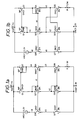
- the basic current mirror circuit has many limitations. One of these is that its impedance is too low for it to act as a perfect current source or sink when connected to other circuitry. To increase the impedance, it is common to include a pair of matched cascode transistors connected respectively to the current mirror transistors. Such a circuit is shown in Figure 1a.
- references Q3 and Q4 denote a first set of matched transistors. Their bases are connected together at the connection point denoted as node 41. In addition, the base of the transistor Q3 is connected to its collector. Reference numerals Q5 and Q6 denote a second set of matched transistors. The transistor Q5 has its collector connected to the emitter of transistor Q3 and its emitter connected to ground. Its base is connected to its own collector at node 42 and to the base of transistor Q6. The transistor Q6 has its collector connected to the emitter of transistor Q4 at node 43 and its emitter connected via a current setting resistor R to ground. Reference numerals Q8 and Q7 denote output transistors connected in cascode for sinking the reference current Ir. Each output transistor has its base connected to receive the base current being injected into the transistor of the associated set (Q8 for Q3 and Q7 for Q5). The circuit is such that the reference current Ir is intended to match a current I flowing through the current setting resistor R.
- Reference numerals Q1 and Q2 denote bias transistors which have their bases connected together and their emitters connected to the supply voltage Vdd. In addition, the base of the transistor Q2 is connected to its collector. The collectors of bias transistors Q1 and Q2 are connected respectively to the collectors of the first matched transistors Q3 and Q4, the latter connection being denoted as node 44.
- the present invention seeks to provide particularly a current source or current sink circuit which can operate down to a relatively low voltage (down to about 1.4 volts) and which has a high DC PSRR (power supply rejection ratio).
- the DC PSRR is defined as the ratio of the change in current source/sink reference current to the change in DC power supply.
- a circuit for providing a reference current comprising:
- the transistors are bipolar n-p-n transistors; the first supply voltage level is a positive value Vdd and the second supply voltage level is ground.
- the bases of the first and second transistors are connected together and the base of the first transistor is connected to its collector.
- the emitters of the third and fourth transistors are connected respectively to the collectors of the first and second transistors and the collector and base of the fourth transistor are connected together.
- the base of the fifth transistor is connected to the collector of the third transistor so as to maintain the collector emitter voltage of the third transistor at a value which is independent of the supply voltage.
- the collector of the fifth transistor is connected to the bias node of the circuit and the emitter of the fifth transistor is connected to the bases of the first and second transistors, which are at a voltage level of one base-emitter voltage Vbe above the second supply voltage level (ground).
- the collector emitter voltage of the third transistor is thus held at 2Vbe above ground and this reduces the so-called "early effect", described later.
- the base of the first transistor is connected to the collector of the second transistor while the base of the second transistor is connected to the collector of the first transistor so that the first and second transistors are cross-coupled.
- the emitter of the fifth transistor is connected to the base of the first transistor.
- the collector of the fourth transistor is connected to its base.
- the bias node for the fifth transistor is provided by two bias transistors each being of opposite type to the first to fifth transistors i.e. p-n-p where the first to fifth transistors are n-p-n and having their emitters connected to the first supply voltage level and their collectors connected respectively to the collectors of the third and fourth transistors.
- the bases of the bias transistors are connected together to provide the bias node for the fifth transistor.
- matched transistors denotes transistors whose collector currents are substantially the same in the same conditions. Other characteristics of the transistor may vary, in particular the base emitter voltages where the transistors are bipolar transistors.
- Figure 1a shows a conventional current mirror circuit which has already been described above with reference to the prior art.
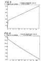
- Figure 5 is a graph which shows the variation in reference current with power supply for such a circuit.
- Figure 1b is a circuit diagram of a circuit which is similar to that of Figure 1a except that the first and second transistors are cross-coupled. That is, the base of the transistor Q5 is connected to the collector of the transistor Q6 and the base of the transistor Q6 is connected to the collector of transistor Q5. With this arrangement, the voltages at nodes 42 and 43 are fixed at 1Vbe above ground, where Vbe is the normal base emitter voltage of a bipolar transistor, typically 0.7V.
- the cross coupling of the transistors Q5,Q6 also minimises the mismatch between the reference current Ir and the set current I as will be described in more detail hereinafter.
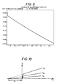
- Figure 10 shows the normal I-V characteristic of a bipolar transistor. That is, Figure 10 shows the variation of collector current Ic with the collector emitter voltage Vce for three different values of base current IB1, IB2 and IB3.
- Va Ic dIc/ dVce and a typical value for Va is 50 to 100V.
- Ic is the collector current
- Is is the saturation current
- Vce is the collector emitter voltage
- Va is the early voltage
- Vbe is the base emitter voltage
- V T is the thermal voltage
- Figure 6 shows the variation of the reference current with power supply for the circuit of Figure 1b.
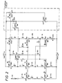
- Figure 2 shows a circuit according to a preferred embodiment of the present invention.
- like numerals designate like parts as in Figures 1a and 1b. That is, there is a first pair of cross-coupled matched transistors Q5,Q6, a second pair of matched transistors Q3,Q4 and a set of two output transistors Q7,Q8. These are connected as described above with reference to Figure 1b.
- the circuit also comprises bias transistors Q1,Q2 each having their emitter connected to a supply voltage Vdd and their collectors connected to respective collectors of the second pair of matched transistors Q3,Q4.
- transistor Q9 having its base connected at node 44 to the collector of one of the second pair of transistors Q3 and having its own collector connected to the bias node 40 provided by the bias transistors Q1,Q2 where their bases are connected together.
- the emitter of the transistor Q9 is connected at the junction of the base of one of the first pair of transistors Q5 and the collector of the other of the first pair of transistors Q6.
- the addition of the transistor Q9 eliminates the so-called early effect by fixing the collector voltage of the transistor Q3 at node 44 to a value which is 2Vbe above ground, VbeQ5+VbeQ9. This effectively fixes the collector emitter voltage of the transistor Q3 at 2Vbe, and thus renders it independent of the supply voltage Vdd.
- the collector current of the transistor Q3 is now independent of variations in the supply voltage Vdd.
- the reproduction at the output transistor Q7 will of course depend on the ratio of areas between Q7 and Q5, as described later.
- VbeQ3 + VbeQ6 + IR VbeQ4 + VbeQ5.
- IR VbeQ4 + VbeQ5 - (VbeQ3 + VbeQ6).
- VceQ6 is set at 1Vbe above ground (by Q5) and VceQ4 is set at 2Vbe above ground (by tying the collector of Q4 to its base and thus to the base of Q3).
- the fixing of Vce of Q3 by Q9 has been explained.
- the equation can be used in its shortened, supply voltage independent form.
- Is1 and Is2 are the saturation currents of Q4 and Q3 respectively.
- A1 is the area ratio between Q3 and Q4 or Q5 and Q6.
- A1 4.
- the reference current generation can be controlled by altering R or A1 depending on requirements.
- a starting circuit is shown indicated by a broken line defining block S.
- This starting circuit comprises a transistor Q10 having its emitter connected to the supply voltage Vdd, its base connected to the junction of the bases of the bias transistors Q1,Q2 and its collector connected to the base of a further transistor Q12.
- the further transistor Q12 has its emitter connected to ground and its collector connected via a resistor R2 to the supply voltage Vdd.
- a start up transistor Q11 has its base connected downstream of the resistor R2, its collector connected to its base and its emitter connected to drive the base of the further transistor Q9 of the current source circuit.
- Figure 3 also shows a capacitor CC for frequency stabilisation purposes between the base and emitter of the transistor Q9.
- Figure 3 is a graph showing the variation in reference current with supply voltage for the circuit of Figure 2.
- Figure 4 shows the current mismatch between the load current I and the reference current Iref as being 20nA at 2V supply.
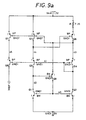
- FIG 7 is a diagram of a circuit according to another embodiment of the present invention which is the same as that of Figure 2 except that the start up circuit is not illustrated and except that the transistors Q5 and Q6 are not cross-coupled but instead are arranged as in the prior art circuit of Figure 1a.
- Figures 9a and 9b are circuit diagrams of circuits arranged to act as a current source of a reference current. Like numerals designate like parts as in Figure 2 and the circuits function in an analagous way and have the same advantages as described above with reference to Figure 2.
- the main function of the transistor Q9 is to hold the collector voltage of Q3 independent of the supply voltage.
- the transistor Q9 could achieve this function with its emitter connected to any of the nodes in the circuit which are set at 1Vbe above ground, particularly node 45 between the output transistors Q7,Q8.
- the only problems which can arise with other connections of Q9 are those of starting up the circuit but these could be overcome with more start up circuitry.
- the circuit can function down to a supply voltage level of 2Vbe+1Vce, i.e. normally 1.7V. However, if different transistors are used having lower Vbe, this would be as low as 1.4V.
Landscapes
- Engineering & Computer Science (AREA)
- Microelectronics & Electronic Packaging (AREA)
- Physics & Mathematics (AREA)
- Nonlinear Science (AREA)
- Electromagnetism (AREA)
- General Physics & Mathematics (AREA)
- Radar, Positioning & Navigation (AREA)
- Automation & Control Theory (AREA)
- Control Of Electrical Variables (AREA)
- Amplifiers (AREA)
Claims (9)
- Circuit pour fournir un courant de référence comprenant :des premier (Q5) et deuxième (Q6) transistors accordés ayant chacun un noeud de commande et un trajet commandable et connectés de sorte que, avec une résistance de réglage de courant (R) dans le trajet commandable du deuxième transistor (Q6), le réglage de courant dans ce trajet commandable est lié à la différence de caractéristique de tension entre les premier (Q5) et deuxième (Q6) transistors et à la valeur de la résistance de réglage de courant (R) ;des troisième (Q3) et quatrième (Q4) transistors accordés ayant chacun un trajet commandable connecté respectivement au trajet commandable des premier (Q5) et deuxième (Q6) transistors et leurs électrodes de commande connectées l'une à l'autre ; etun ensemble de transistors (Q7, Q8) connectés dans le circuit pour être pilotés pour fournir le courant de référence en fonction du courant de réglage,caractérisé en ce que le circuit comprend en outre un cinquième transistor (Q9) connecté dans le circuit avec son trajet commandable entre un noeud de polarisation connecté à un premier niveau de tension d'alimentation (Vdd) et un noeud de réglage à une tension caractéristique par rapport à un second niveau de tension d'alimentation (GND) de façon à maintenir la tension aux bornes de l'un des troisième (Q3) et quatrième (Q4) transistors à une valeur indépendante du premier niveau de tension d'alimentation (Vdd) pour réduire ainsi l'amplitude des variations du courant de référence en fonction de la première tension d'alimentation.
- Circuit selon la revendication 1, dans lequel les premier à cinquième transistors (Q5, Q6, Q3, Q4, Q9) et les transistors de sortie sont des transistors bipolaires et dans lequel chaque caractéristique de tension est la tension base-émetteur d'un transistor.
- Circuit selon la revendication 2, dans lequel les transistors (Q5, Q6, Q3, Q4, Q9) sont des transistors bipolaires NPN et dans lequel le premier niveau de tension d'alimentation est une tension d'alimentation positive (Vdd) et le second niveau de tension d'alimentation est la masse.
- Circuit selon la revendication 2, dans lequel les transistors (Q5, Q6, Q3, Q4, Q9) sont des transistors bipolaires PNP et dans lequel le premier niveau de tension d'alimentation est une tension négative et le second niveau de tension d'alimentation est la masse.
- Circuit selon la revendication 2, dans lequel les transistors (Q5, Q6, Q3, Q4, Q9) sont des transistors bipolaires PNP et dans lequel le premier niveau de tension d'alimentation est la masse et le second niveau de tension d'alimentation est une tension d'alimentation positive (Vdd).
- Circuit selon la revendication 3, dans lequel les premier (Q5) et deuxième (Q6) transistors ont leurs bases connectées l'une à l'autre et la base du premier transistor (Q5) est connectée à son collecteur, et dans lequel la base du cinquième transistor (Q9) est connectée au collecteur du troisième transistor (Q3), l'émetteur du cinquième transistor (Q9) est connecté aux bases des premier (Q5) et deuxième (Q6) transistors, l'émetteur du cinquième transistor (Q5) est connecté à la masse, et l'émetteur du deuxième transistor (Q6) est connecté à la masse par l'intermédiaire de la résistance (R).
- Circuit selon la revendication 3, 4 ou 5, dans lequel la base du premier transitor (Q5) est connectée au collecteur du deuxième transistor (Q6) et la base du deuxième transistor (Q6) est connectée au collecteur du premier transistor (Q5), la base du cinquième transistor (Q9) est connectée au collecteur du troisième transistor (Q3), l'émetteur du cinquième transistor (Q9) est connecté à la base du premier transistor (Q5), l'émetteur du premier transistor (Q5) est connecté au deuxième niveau de tension d'alimentation (GND) et l'émetteur du deuxième transistor (Q6) est connecté, par l'intermédiaire de la résistance (R), au deuxième niveau de tension d'alimentation (GND).
- Circuit selon l'une quelconque des revendications 3 à 7, dans lequel le noeud de polarisation est connecté par deux transistors bipolaires (Q1, Q2) de polarité opposée aux transistors (Q5, Q6, Q3, Q4, Q9), ayant leurs bases connectées ensemble au noeud de polarisation, leurs émetteurs connectés au premier niveau de tension d'alimentation (Vdd) et leurs collecteurs connectés respectivement aux collecteurs des troisième (Q3) et quatrième (Q4) transistors.
- Circuit selon l'une quelconque des revendications 2 à 6, dans lequel la base du quatrième transistor (Q4) est connectée à son collecteur.
Applications Claiming Priority (2)
| Application Number | Priority Date | Filing Date | Title |
|---|---|---|---|
| GB9223338 | 1992-11-06 | ||
| GB929223338A GB9223338D0 (en) | 1992-11-06 | 1992-11-06 | Low voltage reference current generating circuit |
Publications (2)
| Publication Number | Publication Date |
|---|---|
| EP0596653A1 EP0596653A1 (fr) | 1994-05-11 |
| EP0596653B1 true EP0596653B1 (fr) | 1997-08-20 |
Family
ID=10724685
Family Applications (1)
| Application Number | Title | Priority Date | Filing Date |
|---|---|---|---|
| EP93308597A Expired - Lifetime EP0596653B1 (fr) | 1992-11-06 | 1993-10-28 | Circuit générateur de courant de référence à tension faible |
Country Status (5)
| Country | Link |
|---|---|
| US (1) | US5517103A (fr) |
| EP (1) | EP0596653B1 (fr) |
| JP (1) | JP2739732B2 (fr) |
| DE (1) | DE69313244T2 (fr) |
| GB (1) | GB9223338D0 (fr) |
Families Citing this family (13)
| Publication number | Priority date | Publication date | Assignee | Title |
|---|---|---|---|---|
| GB9304954D0 (en) * | 1993-03-11 | 1993-04-28 | Sgs Thomson Microelectronics | Reference current generating circuit |
| DE69427961D1 (de) * | 1994-05-27 | 2001-09-20 | Sgs Thomson Microelectronics | Stromspiegel mit mehreren Ausgängen |
| TW307060B (en) * | 1996-02-15 | 1997-06-01 | Advanced Micro Devices Inc | CMOS current mirror |
| DE19609831A1 (de) * | 1996-03-13 | 1997-09-18 | Philips Patentverwaltung | Schaltungsanordnung zum Liefern eines Gleichstromes |
| JP3610664B2 (ja) * | 1996-03-22 | 2005-01-19 | ソニー株式会社 | ライト電流発生回路 |
| US6002293A (en) * | 1998-03-24 | 1999-12-14 | Analog Devices, Inc. | High transconductance voltage reference cell |
| US6172556B1 (en) * | 1999-03-04 | 2001-01-09 | Intersil Corporation, Inc. | Feedback-controlled low voltage current sink/source |
| ITTO20020252A1 (it) * | 2002-03-21 | 2003-09-22 | Micron Technology Inc | Circuito e procedimento per la generazione di una corrente di riferimento a bassa tensione, dispositivo di memoria comprendente tale circuit |
| US6737849B2 (en) * | 2002-06-19 | 2004-05-18 | International Business Machines Corporation | Constant current source having a controlled temperature coefficient |
| DE102004021232A1 (de) * | 2004-04-30 | 2005-11-17 | Austriamicrosystems Ag | Stromspiegelanordnung |
| JP5326648B2 (ja) * | 2009-02-24 | 2013-10-30 | 富士通株式会社 | 基準信号発生回路 |
| EP2784934B1 (fr) * | 2013-03-25 | 2020-09-23 | Dialog Semiconductor B.V. | Circuit de polarisation électronique destiné à transconductance constante |
| CN115562414A (zh) * | 2022-09-20 | 2023-01-03 | 圣邦微电子(北京)股份有限公司 | 一种电流源 |
Family Cites Families (13)
| Publication number | Priority date | Publication date | Assignee | Title |
|---|---|---|---|---|
| US4119924A (en) * | 1977-09-06 | 1978-10-10 | Rca Corporation | Switchable current amplifiers |
| US4260945A (en) * | 1979-04-06 | 1981-04-07 | Rca Corporation | Regulated current source circuits |
| JPS605085B2 (ja) * | 1980-04-14 | 1985-02-08 | 株式会社東芝 | カレントミラ−回路 |
| JPH0614302B2 (ja) * | 1981-08-20 | 1994-02-23 | 株式会社東芝 | トランジスタ回路 |
| US4558272A (en) * | 1984-07-05 | 1985-12-10 | At&T Bell Laboratories | Current characteristic shaper |
| JPS6369306A (ja) * | 1986-09-11 | 1988-03-29 | Seikosha Co Ltd | 電流ミラ−回路 |
| JPH0682309B2 (ja) * | 1987-01-23 | 1994-10-19 | 松下電器産業株式会社 | 基準電圧発生回路 |
| JPS63234307A (ja) * | 1987-03-24 | 1988-09-29 | Toshiba Corp | バイアス回路 |
| US4792748A (en) * | 1987-11-17 | 1988-12-20 | Burr-Brown Corporation | Two-terminal temperature-compensated current source circuit |
| US4879524A (en) * | 1988-08-22 | 1989-11-07 | Texas Instruments Incorporated | Constant current drive circuit with reduced transient recovery time |
| FR2655791A1 (fr) * | 1989-12-13 | 1991-06-14 | Siemens Automotive Sa | Circuit de miroir de courant corrige de l'effet early. |
| JPH0535350A (ja) * | 1991-07-26 | 1993-02-12 | Nec Yamagata Ltd | 定電流源 |
| US5349286A (en) * | 1993-06-18 | 1994-09-20 | Texas Instruments Incorporated | Compensation for low gain bipolar transistors in voltage and current reference circuits |
-
1992
- 1992-11-06 GB GB929223338A patent/GB9223338D0/en active Pending
-
1993
- 1993-08-12 US US08/105,450 patent/US5517103A/en not_active Expired - Lifetime
- 1993-10-28 DE DE69313244T patent/DE69313244T2/de not_active Expired - Fee Related
- 1993-10-28 EP EP93308597A patent/EP0596653B1/fr not_active Expired - Lifetime
- 1993-11-05 JP JP5277112A patent/JP2739732B2/ja not_active Expired - Fee Related
Also Published As
| Publication number | Publication date |
|---|---|
| JP2739732B2 (ja) | 1998-04-15 |
| JPH07146725A (ja) | 1995-06-06 |
| DE69313244T2 (de) | 1998-03-26 |
| DE69313244D1 (de) | 1997-09-25 |
| EP0596653A1 (fr) | 1994-05-11 |
| GB9223338D0 (en) | 1992-12-23 |
| US5517103A (en) | 1996-05-14 |
Similar Documents
| Publication | Publication Date | Title |
|---|---|---|
| JP2549540B2 (ja) | レベルシフト回路 | |
| US4961046A (en) | Voltage-to-current converter | |
| EP0596653A1 (fr) | Circuit générateur de courant de référence à tension fAIble | |
| US5576616A (en) | Stabilized reference current or reference voltage source | |
| US4591804A (en) | Cascode current-source arrangement having dual current paths | |
| JPS635923B2 (fr) | ||
| EP0363298B1 (fr) | Circuit logique à commutateurs de courant avec signaux de sortie dont les niveaux sont commandés | |
| US4491780A (en) | Temperature compensated voltage reference circuit | |
| US4786856A (en) | Temperature compensated current source | |
| US4292583A (en) | Voltage and temperature stabilized constant current source circuit | |
| US4317082A (en) | Current mirror circuit | |
| EP0456127B1 (fr) | Amplificateur | |
| EP0435335B1 (fr) | Circuit de transistor et circuit convertisseur de niveau | |
| US5592123A (en) | Frequency stability bootstrapped current mirror | |
| US5349307A (en) | Constant current generation circuit of current mirror type having equal input and output currents | |
| JPH0480406B2 (fr) | ||
| JP2002525738A (ja) | 電圧及び/又は電流基準回路 | |
| US4553106A (en) | Output stage for an operational amplifier | |
| US4254381A (en) | Balanced-to-single-ended signal converters | |
| EP0615182A2 (fr) | Circuit générateur de courant de référence | |
| JPH0434567Y2 (fr) | ||
| JPH04338811A (ja) | バンドギャップ基準電圧発生回路 | |
| JPH0522275B2 (fr) | ||
| JPS645369Y2 (fr) | ||
| JPS5841683B2 (ja) | 電流増幅回路 |
Legal Events
| Date | Code | Title | Description |
|---|---|---|---|
| PUAI | Public reference made under article 153(3) epc to a published international application that has entered the european phase |
Free format text: ORIGINAL CODE: 0009012 |
|
| AK | Designated contracting states |
Kind code of ref document: A1 Designated state(s): DE FR GB IT |
|
| 17P | Request for examination filed |
Effective date: 19940620 |
|
| 17Q | First examination report despatched |
Effective date: 19960305 |
|
| GRAG | Despatch of communication of intention to grant |
Free format text: ORIGINAL CODE: EPIDOS AGRA |
|
| GRAH | Despatch of communication of intention to grant a patent |
Free format text: ORIGINAL CODE: EPIDOS IGRA |
|
| GRAH | Despatch of communication of intention to grant a patent |
Free format text: ORIGINAL CODE: EPIDOS IGRA |
|
| GRAA | (expected) grant |
Free format text: ORIGINAL CODE: 0009210 |
|
| AK | Designated contracting states |
Kind code of ref document: B1 Designated state(s): DE FR GB IT |
|
| REF | Corresponds to: |
Ref document number: 69313244 Country of ref document: DE Date of ref document: 19970925 |
|
| ET | Fr: translation filed | ||
| PLBE | No opposition filed within time limit |
Free format text: ORIGINAL CODE: 0009261 |
|
| 26N | No opposition filed | ||
| REG | Reference to a national code |
Ref country code: GB Ref legal event code: IF02 |
|
| PGFP | Annual fee paid to national office [announced via postgrant information from national office to epo] |
Ref country code: DE Payment date: 20021031 Year of fee payment: 10 |
|
| PG25 | Lapsed in a contracting state [announced via postgrant information from national office to epo] |
Ref country code: DE Free format text: LAPSE BECAUSE OF NON-PAYMENT OF DUE FEES Effective date: 20040501 |
|
| PGFP | Annual fee paid to national office [announced via postgrant information from national office to epo] |
Ref country code: FR Payment date: 20041008 Year of fee payment: 12 |
|
| PGFP | Annual fee paid to national office [announced via postgrant information from national office to epo] |
Ref country code: GB Payment date: 20041027 Year of fee payment: 12 |
|
| PG25 | Lapsed in a contracting state [announced via postgrant information from national office to epo] |
Ref country code: IT Free format text: LAPSE BECAUSE OF NON-PAYMENT OF DUE FEES Effective date: 20051028 Ref country code: GB Free format text: LAPSE BECAUSE OF NON-PAYMENT OF DUE FEES Effective date: 20051028 |
|
| GBPC | Gb: european patent ceased through non-payment of renewal fee |
Effective date: 20051028 |
|
| PG25 | Lapsed in a contracting state [announced via postgrant information from national office to epo] |
Ref country code: FR Free format text: LAPSE BECAUSE OF NON-PAYMENT OF DUE FEES Effective date: 20060630 |
|
| REG | Reference to a national code |
Ref country code: FR Ref legal event code: ST Effective date: 20060630 |