EP0596740B1 - Schaltung und Verfahren zum Betreiben von Starkentladungslampen durch Rückwirkung - Google Patents
Schaltung und Verfahren zum Betreiben von Starkentladungslampen durch Rückwirkung Download PDFInfo
- Publication number
- EP0596740B1 EP0596740B1 EP93308832A EP93308832A EP0596740B1 EP 0596740 B1 EP0596740 B1 EP 0596740B1 EP 93308832 A EP93308832 A EP 93308832A EP 93308832 A EP93308832 A EP 93308832A EP 0596740 B1 EP0596740 B1 EP 0596740B1
- Authority
- EP
- European Patent Office
- Prior art keywords
- lamp
- current
- error signal
- bus voltage
- signal
- Prior art date
- Legal status (The legal status is an assumption and is not a legal conclusion. Google has not performed a legal analysis and makes no representation as to the accuracy of the status listed.)
- Expired - Lifetime
Links
Images


Classifications
-
- H—ELECTRICITY
- H05—ELECTRIC TECHNIQUES NOT OTHERWISE PROVIDED FOR
- H05B—ELECTRIC HEATING; ELECTRIC LIGHT SOURCES NOT OTHERWISE PROVIDED FOR; CIRCUIT ARRANGEMENTS FOR ELECTRIC LIGHT SOURCES, IN GENERAL
- H05B41/00—Circuit arrangements or apparatus for igniting or operating discharge lamps
- H05B41/14—Circuit arrangements
- H05B41/36—Controlling
- H05B41/38—Controlling the intensity of light
- H05B41/39—Controlling the intensity of light continuously
- H05B41/392—Controlling the intensity of light continuously using semiconductor devices, e.g. thyristor
-
- H—ELECTRICITY
- H05—ELECTRIC TECHNIQUES NOT OTHERWISE PROVIDED FOR
- H05B—ELECTRIC HEATING; ELECTRIC LIGHT SOURCES NOT OTHERWISE PROVIDED FOR; CIRCUIT ARRANGEMENTS FOR ELECTRIC LIGHT SOURCES, IN GENERAL
- H05B41/00—Circuit arrangements or apparatus for igniting or operating discharge lamps
- H05B41/14—Circuit arrangements
- H05B41/26—Circuit arrangements in which the lamp is fed by power derived from DC by means of a converter, e.g. by high-voltage DC
- H05B41/28—Circuit arrangements in which the lamp is fed by power derived from DC by means of a converter, e.g. by high-voltage DC using static converters
- H05B41/288—Circuit arrangements in which the lamp is fed by power derived from DC by means of a converter, e.g. by high-voltage DC using static converters with semiconductor devices and specially adapted for lamps without preheating electrodes, e.g. for high-intensity discharge lamps, high-pressure mercury or sodium lamps or low-pressure sodium lamps
- H05B41/2881—Load circuits; Control thereof
- H05B41/2882—Load circuits; Control thereof the control resulting from an action on the static converter
- H05B41/2883—Load circuits; Control thereof the control resulting from an action on the static converter the controlled element being a DC/AC converter in the final stage, e.g. by harmonic mode starting
-
- Y—GENERAL TAGGING OF NEW TECHNOLOGICAL DEVELOPMENTS; GENERAL TAGGING OF CROSS-SECTIONAL TECHNOLOGIES SPANNING OVER SEVERAL SECTIONS OF THE IPC; TECHNICAL SUBJECTS COVERED BY FORMER USPC CROSS-REFERENCE ART COLLECTIONS [XRACs] AND DIGESTS
- Y10—TECHNICAL SUBJECTS COVERED BY FORMER USPC
- Y10S—TECHNICAL SUBJECTS COVERED BY FORMER USPC CROSS-REFERENCE ART COLLECTIONS [XRACs] AND DIGESTS
- Y10S315/00—Electric lamp and discharge devices: systems
- Y10S315/07—Starting and control circuits for gas discharge lamp using transistors
Definitions
- the present invention relates to the field of power supplies for high intensity discharge lamps, and more particularly to power supplies using feedback control for regulating voltage or current supplied to a lamp.
- HPSL high pressure sodium lamp
- HPSLs high pressure sodium lamps
- One problem with HPSLs is the considerable drift in lamp impedance that normally occurs as the lamp ages. Such impedance drift is due to such factors as outgassing of the active lamp element sodium into an arc tube that houses the sodium.
- the drift in impedance value is upwards, causing a lamp with increasing usage to require increasingly greater power, eventually exceeding the capacity of its power supply circuit, and resulting in lamp failure.
- Variations in impedance from lamp to lamp also occur from usual manufacturing tolerances. Using the same lamp driving voltage, for instance, such impedance variations cause variations amongst lamps in both lumen output and spectrum of light wavelengths emitted (i.e., the color of light produced). Similar variations in lamp characteristics can also result from changes in line voltages for even the same lamp.
- the '038 patent employs a power switch that applies a d.c. bus, or compliance, voltage across the series combination of lamp and a driver, or ballast, inductor when the switch is on, or conducting.
- a d.c. bus or compliance
- the lamp is isolated from the bus voltage, and lamp current is then controlled by the impedance of the driver inductor and the internal lamp impedance.
- the average current through the power switch is measured, and in a feedback loop, an "error" signal is generated that essentially represents the difference between the average switch current and a set point for the current.
- the error signal is then used to control the on-off operation of the power switch so as to minimize the error signal.
- the set point itself may be dynamic, and responsive to variations in the d.c. bus voltage caused by variations of line voltage of an a.c. supply.
- EP-A-0 596 739 entitled “Circuit and Method for Operating High Pressure Sodium Vapor Lamps", by Kachmarik et al and to EP-A-0 596 741 "High-Pressure Sodium Lamp Control Circuit Providing Constant Peak Current and Color”.
- an object of the invention is to provide a feedback-controlled circuit and method for powering a high intensity discharge lamp that achieves a desired power level in the lamp despite considerable changes in the value of lamp impedance.
- Another object of the invention is to provide a feedback-controlled circuit and method of the foregoing type that also achieves a nearly constant amplitude of driving current for the lamp.
- a further object is to provide circuits and methods of the foregoing several types that can be implemented with low cost, readily available circuit components.
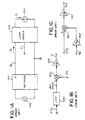
- Fig. 1A is a schematic diagram partly in block form representing a prior art electrical circuit for regulating lamp power
- Figs. 18 and 1C are circuit diagrams partly in block form of portions of a feedback loop used with the circuit of Fig. 1A.
- Fig. 2A is a detail schematic diagram of a lamp driver circuit shown in block form in Fig. 1A, and Figs. 28 and 2C show waveforms of various currents in the circuit of Fig. 2A.
- Fig. 3A is a schematic diagram partly in block form of an electrical circuit for powering a lamp in accordance with the invention
- Figs. 38 and 3C are respective circuit diagrams partly in block form of a pair of feedback loops used with the circuit of Fig. 3A.
- Fig. 4A is a detail schematic diagram of a bus-voltage regulating circuit and a lamp-driver circuit shown in block form in Fig. 3A, and Fig. 48 shows waveforms of current and voltage from the lamp driver circuit of Fig. 4A.
- Fig. 5 is a graph of lamp power versus lamp impedance for an embodiment of the invention.
- Fig. 1A shows a simplified schematic of a circuit for powering a high intensity discharge lamp 100, such as a high pressure sodium lamp (HPSL).
- a bus voltage V B also known as the link, or compliance, voltage comprises the d.c. output voltage of a full-wave bridge rectifier 104, whose current output is I B .
- Rectifier 104 is supplied with a.c. power by source 106.
- a standard power correction circuit (not shown) may be placed in the current path between rectifier 104 and a.c. source 106.
- a lamp driver circuit 108 supplied with the bus voltage V B and bus current I B , "drives" lamp 100 with suitable voltage or current waveforms, as described below, for regulating lamp power towards a constant value.
- Lamp driver 108 is controlled by a feedback error signal E, produced by the feedback loop shown in Fig. 1B.
- a low pass filter 120 receives signal ⁇ I S proportional to a current I S described below, where ⁇ indicates proportionality.
- Low pass filter 120 outputs a time-averaged value of ⁇ I S to the positive input of a standard summing amplifier 122.
- the negative input of the summing amplifier is fed with a target value, or set point, SP 1 for average current, which may be non-dynamic.
- the output of the summing amplifier 122 scaled by a gain G 1 of an amplifier 124, constitutes the error signal E to which lamp driver 108 responds to regulate the average lamp power towards a constant value.
- Fig. 1C shows an enhancement to the feedback loop of Fig. 1B to compensate for variations in the d.c. bus voltage V B caused by variations in the line voltage of the a.c. source 106 (Fig. 1A).
- the Fig. 1C circuit makes the set point SP 1 , used in feedback loop 120 of Fig. 1B, a dynamic signal.
- the signal SP 1 is the output of a standard summing amplifier 140 as scaled by gain G 2 of an amplifier 142.
- the positive input of summing amplifier 140 is a non-dynamic set point SP 2 , and its negative input is the bus voltage V B as scaled by gain G 3 of amplifier 144.
- FIG. 1A Further details of lamp driver 108 (Fig. 1A) are shown in the detail view of Fig. 2A.
- the circuit of Fig. 2A can comprise part of an inventive combination of elements, and for this reason Fig. 2A and associated Figs. 2B and 2C are not labelled Prior Art.
- error signal E is received by a gate control circuit 200 for controlling the on (conducting) and off (non-conducting) states of a power field-effect transistor (FET), or other power switch, 202 of lamp driver 108.
- FET field-effect transistor
- a gate control circuit 200 for controlling the on (conducting) and off (non-conducting) states of a power field-effect transistor (FET), or other power switch, 202 of lamp driver 108.
- FET power field-effect transistor
- the current in power switch 202 i.e., current I S
- I S the current in power switch 202
- the bus current I B when diode D is non-conducting, and both are zero when switch 202 is off and diode D conducts.
- the switch current I S and the bus current I B are the same in the circuit shown.
- the switch current I S (and hence the bus current I B ) is measured by means of resistor R, through which switch current I S flows.
- the voltage V R is the signal ⁇ I S that is applied to low pass filter 120 of Fig. 1B.
- Gate control circuit 200 (Fig. 2A) controls the on and off operation of switch 202 to create the current waveforms shown in Fig. 2B.
- the solid-line curve represents switch current I S , and comprises a series of N trapezoidal pulses 220 in a duty cycle period T that is constant, followed by another series of N pulses 222 in a succeeding duty cycle period, also T.
- T duty cycle period
- Below the time axis are shown the on and off timing cycles for the switch 202.
- the first two pulses of pulse series 220 are shown in the detail view of Fig. 2C.
- the first pulse in series 220 ramps from zero to a preset maximum value (curve 240), during which time the switch current is common with, or the same as, the lamp current I L .
- curve 240 a preset maximum value
- switch 202 is turned off, causing the switch current I S to fall rapidly to zero (curve 242).
- the lamp current I L decays through inductor L (Fig.
- switch 202 is again turned on, the switch current I S rises rapidly along curve 246, and then, together with the then-common lamp current I L , ramps along curve 248 to the maximum value.
- Switch 202 is cyclically operated in this manner to create series 220 of N pulses.
- Fig. 2B shows the next series of pulses 222, also comprising N in number, but occurring in a shorter time interval W 2 than interval W 1 of the first series 220. Achieving the shorter interval W 2 results from switching switch 202 at a higher frequency during pulse series 222 than during series 220. Because the lengths of intervals W 1 , W 2 , etc. constitute the active portions of a constant-period (T) duty cycle for driving the lamp, adjusting the lengths of such intervals W 1 , W 2 , etc. regulates the average current in the lamp.
- T constant-period
- lamp driver 108 of Fig. 2A and especially of gate control circuit 200, are disclosed in the subject prior art '038 patent, particularly in relation to Fig. 3 of that patent.
- lamp power is essentially proportional to the mathematical product of the d.c. bus voltage V B , assumed constant for mathematical analysis, and the dynamic average value of switch current I S (Fig. 2A). This may be represented mathematically as follows: P L ⁇ V B (AVE. I S ), where
- the instant invention regulates lamp power in a way that more fully compensates for the increasing impedance over time of a lamp, such as a HPSL.
- Figs. 3A-3C show a circuit for regulating power of a high intensity discharge lamp 300, such as a high pressure sodium lamp (HPSL).
- a full-wave bridge rectifier 304 translates a.c. voltage from a.c. source 306 to a d.c. voltage appearing across the "+" and "-" output terminals of the rectifier.
- V B regulator 320 is feedback controlled by an error signal E 1 , which is distinct from error signal E 2 supplied to lamp driver 308.
- a current-to-voltage converter 330 includes a transformer 400, shown in Fig. 4A, which conducts on its primary winding the lamp current I L and on its secondary winding, a current ⁇ I L , where ⁇ indicates the proportionality of the secondary-to-primary winding turns ratio of the transformer.
- Current-to-voltage converter 330 produces an output with a conversion gain H 2 , which incorporates the mentioned winding turns ratio.
- the output of converter 330 is further scaled by gain H 1 of amplifier 332 before reaching a peak-hold circuit 334.
- the output of the peak-hold circuit on line 336 which output is proportional to the peak value of the lamp current I L , has subtracted from it at a standard summing amplifier 338 a set point value SP 1 , to produce error signal E 1 as the output of the summing amplifier.
- V B regulator 320 (Fig. 3A), which responds to error signal E 1 , is shown in more detail in Fig. 4A.
- V B regulator 320 may utilize a standard ML4813CP integrated circuit (IC) 402, which is assumed for the following description.
- IC 402 As specified, summing amplifier 338 of the feedback loop of Fig. 3B is internal to the IC.
- pin 8 of IC 402 corresponds to line 336 shown in Fig. 3B, and pin 7 of the IC corresponds to the negative input to summing amplifier 338 (Fig. 3B).
- the set point SP 1 is conveniently provided on pin 7 of IC 402 by a reference voltage V r , which may be non-dynamic.
- IC 402 typically further includes a standard power factor control circuit 404, responsive to the error signal E 1 and whose output represents a modified error signal used in IC 402 for controlling the duty cycle, or on-off operation, of a power switch 414. Power factor control of 0.99 has been attained in this manner.
- Secondary current flowing through a transformer 406 indirectly indicates the regulated bus voltage REG. V B , such secondary current being substantially proportional to such voltage. This is because the amount of current charges "pumped" into capacitor 410 via diode 412 and transformer 406 when switch 414 is off determines the value of the regulated bus voltage REG. V B on capacitor 410. The timing of on and off operation of switch 414, determined by the output of IC 402 on pin 12, thus controls the value of the regulated bus voltage REG. V B .
- capacitor 410, diode 412 and switch 414 comprise a buck-boost circuit 416 of standard construction for regulating the regulated bus voltage REG. V B as needed and which, if necessary, causes REG. V B to rise above the d.c. bus voltage supplied by rectifier 304 (Fig. 3A).
- V B regulator 320 provides a regulated bus voltage REG. V B that is nearly constant in contrast to the frequency of operation of the succeeding-stage lamp driver 308. As described below, the provision of the regulated bus voltage REG. V B results in a nearly constant amplitude of current used to drive lamp 300. In a HPSL, this results in lamp 300 consistently exhibiting a desired color spectrum. Additionally, V B regulator 320 compensates for considerable changes in the line voltage of a.c. supply 306.
- Fig. 3C shows a feedback loop used to produce error signal E 2 , to which lamp driver 308 of Fig. 3A is responsive.
- a standard summing amplifier 350 receives its negative input from a feedback branch that receives a signal I B ' as the input to a current-to-voltage converter 330'.
- the average value of signal I B ' at least approximates the average bus current I B .
- the output of converter 330' represents the signal I B ' scaled by conversion gain H 2 of the converter.
- a low pass filter 351 then time averages the output of converter 330', providing the averaged value to the negative input of summing amplifier 350.
- signal I B ' received by current-to-voltage converter 330' may be the bus current I B , which, in the Fig. 2A embodiment, is common with the switch current I S .
- Signal I B ' may also be the lamp current I L , whose average value approximates the average value of the bus current I B . If the lamp current I L is input into converter 330', converter 330 of Fig. 3B can be the same as converter 330'.
- the input of an amplifier 352 is substantially proportional to the regulated bus voltage REG. V B , and may comprise the secondary winding current from transformer 406 (Fig. 4A), which, as described above, indirectly indicates the regulated bus voltage REG. V B .
- the secondary winding current of transformer 406, specifically, is substantially proportional to (N S /N P )(REG. V B ), where REG. V B is the regulated bus voltage and N S /N P is the secondary-to-primary turns ratio of transformer 406.
- Amplifier 352 is preferably configured to receive its input current from transformer 406 through an input resistor (not shown) connected to the negative input of an operational amplifier (not shown), which input, in turn, is connected to the output of such amplifier through a feedback resistor (not shown).
- the gain m of amplifier 352 is then the ratio of the feedback resistance divided by the input resistance.
- the positive input of such operational amplifier may then be connected to pins 5 and 15 (not shown) of an IC 470 comprising a MC34066P chip, as described below.
- the output of amplifier 352 is (REG. V B )(N S /N P )m, where m is the gain of amplifier 352; such output is applied as a negative input to a standard summing amplifier 354.
- the positive input of amplifier 354 is a set point SP 2 , which may be non-dynamic.
- the value of set point SP 2 is referred to herein as K, and may be non-dynamic.
- the output of summing amplifier 354 is scaled by gain a in amplifier 356 to produce a dynamic set point SP 3 , which is applied as the positive input to summing amplifier 350.
- the output of amplifier 350 is the error signal E 2 .
- a so-called offset voltage V O whose value may be positive or negative, typically exists between the positive and negative inputs of amplifier 350.
- FIG. 3A A mathematical analysis of the feedback loops shown in Figs. 3B and 3C shows, for instance, their ability to compensate for considerable changes in the impedance Z L of lamp 300 (Fig. 3A), a desirable trait for long lamp life.
- the average lamp current AVE. I L in equations 3 and 4 can be replaced by AVE. I B ', where AVE. I B ' at least approximates the average value of the bus current I B .
- PEAK I L (SP 1 )/(H 2 H 1 ), where
- Equation 9 shows that the dynamic set point SP 3 is dependent on parameters of the feedback circuits of Figs. 3B and 3C, which are typically constant, the driver impedance Z D , also typically constant, and the lamp impedance Z L , which changes considerably as a HPSL ages. Since the set point SP 3 changes with changes in lamp impedance, the invention compensates for considerable changes in lamp impedance.
- Fig. 5 graphically illustrates.
- solid-line curve 500 is plotted in watts of power versus lamp impedance Z L in ohms.
- its impedance Z L increases considerably.
- the invention achieves the rounded trajectory shown at 502, whereby the circuit powering the lamp is longer able to supply the needed power to operate the lamp.
- a lamp's power-versus-impedance curve has the continuing trajectory of dashed-line curve 504, and the lamp's power supply circuit more quickly becomes incapable of supplying the needed power to operate the lamp.
- Error signal E 2 is applied to lamp driver 308 (Fig. 3A), which may take the form as previously described in connection with Fig. 2A and the associated current waveforms of Figs. 2B and 2C.
- Lamp driver 308 is shown in Fig. 4A.
- lamp driver 308 is configured with a pair of switches 450 and 452 whose on-off operation is complementary such that switch 450 is on while switch 452 is off, and vice versa.
- the lamp voltage V L and lamp current I L are plotted in Fig. 4B. Assuming the lamp voltage V L is initially zero, turning on switch 450 causes the regulated bus voltage REG. V B to be impressed across the series combination of a resonant inductor 454, lamp 300, and resonant capacitor 456, neglecting the low impedance of lamp current-sensing transformer 400. Since the lamp is extinguished at this time, the full regulated bus voltage REG. V B appears across the lamp, as indicated by the rapidly rising curve 480 in Fig. 4B.
- Such abrupt rise in lamp voltage V L forces a re-ignition of the lamp. This, in turn, initiates a lamp current having a resonant frequency primarily determined by the principal inductive and capacitive elements in the current path, which are resonant inductor 454 and parallel-connected resonant capacitors 456 and 458.
- the resonating lamp current I L causes the lamp voltage V L to resonate towards 2(REG. V B ), until it is clamped to the sum of REG. V B and the voltage drop across one of diodes 460 and 462. This point corresponds to ⁇ /2 radians, or 1/4 of the resonant cycle, where the lamp current (curve 482) reaches its maximum value. At this point, the resonant portion of the cycle has ended.
- the lamp voltage V L is clamped by one of diodes 460 and 462, and the energy stored in inductor 454 discharges as an exponential decay into the bus. Once the lamp current I L has decayed to zero, switch 450 can be turned off.
- Lamp driver 308 is now prepared to begin the cycle in the opposite direction because common node 465 between diodes 460 and 462 reaches the value of the regulated bus voltage REG. V B .
- the amount of "dead time" is determined by the error signal E 2 and the responsive circuitry for controlling the on-off operation of switches 450 and 452, described below.
- switch 452 can be turned on. As with the previous cycle, the entire REG. V B is placed across lamp 300 until it re-ignites. Once this occurs, the lamp current begins to oscillate in the opposite direction of the described current flow through switch 450. During this time, the lamp voltage V L begins to resonate downward toward the negative value of the regulated bus voltage, - REG. V B , until it is clamped at the negative voltage across one of diodes 460 and 462. At this point the forcing current is at its maximum negative value. As before, the process is the same, only the direction of current has changed.
- Switches 450 and 452 are operated to achieve the waveforms of Fig. 4B in response to error signal E 2 received at pin 3 of IC 470 when embodied as a standard MC34066P chip, which is assumed in the following description.
- Error signal E 2 thereby controls the frequency of a signal on the primary winding 471 of a transformer 472, such primary winding 471 being connected and poled in the manner shown to output pins 12 and 14 of IC 470.
- Secondary winding 474 of transformer 472 is poled and connected to control the control the on-off operation of switch 450, which may be a FET. Where switch 450 is a FET, secondary winding 472 is connected across its gate and source terminals.
- a further secondary winding 476 is poled and connected as shown to control switch 452, which may also be a FET. Because secondary windings 474 and 476 are oppositely poled, a positive waveform through the primary winding of transformer 472 turns on only one of the switches, and a negative waveform through the primary winding turns on only the other of the switches.
- lamp driver circuit 308 Further details of lamp driver circuit 308 are contained in the above cross-referenced application, attorney docket no. LD-10,203, the entire disclosure of which is incorporated herein by reference.
- Fig. 4A circuit for a 95-watt HPSL 300 uses the following component values: inductance of transformer 406 in series with diode 412, 172 microhenries; capacitor 410, 470 microfarads; N S /N P of transformer 406, 6/45; resonant inductor 454, 500 microhenries; resonant capacitors 456 and 458, each 4 microfarads; and ICs 402 and 470, the ICs identified by number above. Using such values, one possible implementation of the feedback loops of Figs.
- 3B and 3C are as follows: gain H 1 , 5.236; gain H 2 , 80.65 X 10 -3 ; set point SP 1 , 5.0; gain m, 95.3 X 10 -3 ; set point SP 2 (i.e. K), 5.477; gain a, 14 X 10 -3 ; and offset voltage V O , 0.
- the invention provides compensation for considerable variance in lamp impedance while maintaining a nearly constant power level. It also provides a nearly constant amplitude of lamp current, and the ability to compensate for considerable variations of the a.c. line voltage. Further, these features may be attained with low cost, readily available circuit components.
Landscapes
- Engineering & Computer Science (AREA)
- Power Engineering (AREA)
- Circuit Arrangements For Discharge Lamps (AREA)
- Inverter Devices (AREA)
Claims (10)
- Schaltungsanordnung zum Speisen einer Hochintensitäts-Entladungslampe (300), enthaltend :a) eine Einrichtung (304) zum Liefern einer Bus-Gleichspannung (VB),b) eine erste geregelte Einrichtung, um auf einem einen Bus-Strom (IB) liefernden Leiter die Bus-Spannung (VB) als Antwort auf ein erstes Fehlersignal in der Weise zu regeln, daß das erste Fehlersignal minimiert wird, wobei das erste Fehlersignal im wesentlichen proportional zu der Differenz zwischen (1) einem dynamischen Signal, das im wesentlichen proportional zu dem Lampenspitzenstrom ist, und (2) zu einem Sollwertsignal für den Lampenspitzenstrom proportional ist, undc) eine zweite geregelte Einrichtung zum Versorgen der Lampe (300) mit der geregelten Bus-Spannung (VB) als Antwort auf ein zweites Fehlersignal in der Weise, daß das zweite Fehlersignal minimiert ist und dadurch die Leistung in der Lampe geregelt wird, wobei das zweite Fehlersignal im wesentlichen proportional zu der Differenz zwischen (1) einem dynamischen Signal, das im wesentlichen proportional zu dem mittleren Bus-Strom ist, und (2) einem dynamischen Sollwertsignal ist, das im wesentlichen proportional zu der Differenz zwischen (i) einem dynamischen Signal, das im wesentlichen proportional zu der geregelten Bus-Spannung ist, und (ii) einem Sollwertsignal ist, das mit der Lampenleistung in Beziehung steht.wobei die zweite geregelte Einrichtung enthält:a) einen derart geschalteten Leistungsschalter, daß die geregelte Bus-Spannung einer Reihenschaltung, die die Lampe und eine Drossel enthält, aufgedrückt wird, wenn der Schalter eingeschaltet ist, und die Reihenschaltung von der geregelten Bus-Spannung getrennt wird, wenn der Schalter ausgeschaltet ist, undb) eine Schaltersteuereinrichtung zum wiederholten Ein- und Ausschaltung des Leistungsschalters in der Weise, daß das zweite Fehlersignal minimiert ist.
- Schaltungsanordnung nach Anspruch 2, wobei die zweite geregelte Einrichtung so aufgebaut ist, daß die Frequenz des wiederholten Ein- und Ausschaltens des Leistungsschalters die Länge von einem aktiven Abschnitt von einem eine konstante Periode aufweisenden Tastverhältnis zum Versorgen der Lampe bestimmt.
- Schaltungsanordnung nach Anspruch 1, wobei die erste geregelte Einrichtung eine Zusatzschaltung (buck-boost circuit) mit einem Schalter aufweist, dessen Ein-Aus-Betrieb als Antwort auf das erste Fehlersignal gesteuert wird, um so das Signal zu minimieren.
- Schaltungsanordnung nach Anspruch 1, wobei die zweite geregelte Einrichtung enthält:a) erste und zweite Stromschleifen, die so angeordnet sind, daß sie Strom durch die Lampe in entsprechenden ersten und zweiten entgegengesetzten Richtungen leiten,b) erste und zweite Leistungsschalter zum sequentiellen Anordnen der Lampe abwechselnd in den ersten und zweiten Stromschleifen, undc) wobei die ersten und zweiten Stromschleifen jeweils induktive und kapazitive Elemente aufweisen, die so gewählt sind, daß entsprechende erst und zweite Schleifenstromkurven jeweils einen in Resonanz schwingenden Abschnitt aufweisen, der hauptsächlich durch den Wert der induktiven und kapazitiven Elemente bestimmt ist.
- Verfahren zum Speisen einer Hochintensitäts-Entladungslampe (300), enthaltend:Liefern einer Bus-Gleichspannung (VB),Regeln der Bus-Spannung (VB) als Antwort auf ein erstes Fehlersignal in der Weise, daß das erste Fehlersignal minimiert wird, wobei das erste Fehlersignal im wesentlichen proportional zu der Differenz zwischen (1) einem dynamischen Signal, das im wesentlichen proportional zu dem Lampenspitzenstrom ist, und (2) einem Sollwertsignal für den Lampenspitzenstrom ist, undVersorgen der Lampe (300) mit der geregelten Bus-Spannung (VB) als Anwort auf ein zweites Fehlersignal in der Weise, daß das zweite Fehlersignal minimiert und dadurch die Leistung in der Lampe geregelt wird, wobei das zweite Fehlersignal im wesentlichen proportional zu der Differenz zwischen (1) einem dynamischen Signal, das im wesentlichen proportional zu einem mittleren Bus-Strom ist, und (2) einem dynamischen Sollwertsignal ist, das im wesentlichen proportional zu der Differenz zwischen (i) einem dynamischen Signal, das im wesentlichen proportional zu der geregelten Bus-Spannung ist, und (ii) einem Sollwertsignal ist, das mit der Lampenleistung in Beziehung steht.wobei der Schritt zum Versorgen der Lampe enthält:alternatives Aufdrücken der geregelten Bus-Spannung über eine Reihenschaltung, die die Lampe und eine Drossel enthält, und dann Trennen der Reihenschaltung von der geregelten Bus-Spannung, undSteuern der Frequenz des alternativen Aufdrückens und Trennens der Reihenschaltung von der geregelten Bus-Spannung, um so das zweite Fehlersignal zu minimieren.
- Verfahren nach Anspruch 7, wobei der Schritt der Steuerung der Frequenz des alternativen Aufdrückens und Trennens der Reihenschaltung von der geregelten Bus-Spannung eine auf die Frequenz ansprechende Länge von einem aktiven Abschnitt von einem eine konstante Periode aufweisenden Tastverhältnis zum Versorgen der Lampe bestimmt.
- Verfahren nach Anspruch 6, wobei der Schritt des Erzeugens der geregelten Bus-Spannung enthält, daß der Ein-Aus-Betrieb von einer Zusatzschaltung gesteuert wird, deren Ausgangsgröße die geregelte Bus-Spannung ist, um so das erste Fehlersignal zu minimieren.
- Schaltungsanordnung nach einem der Ansprüche 1 bis 5 oder Verfahren nach einem der Ansprüche 6 bis 9, wobei das Sollwertsignal für den Spitzenlampenstrom oder das Sollwertsignal in Bezug auf die Lampenleistung nicht-dynamisch ist.
- Schaltungsanordnung nach einem der Ansprüche 1 bis 5 oder Verfahren nach einem der Ansprüche 6 bis 9, wobei das dynamische Signal, das im wesentlichen proportional zu dem mittleren Bus-Strom ist, vom Messen des Stroms in der Lampe abgeleitet ist.
- Verfahren nach Anspruch 6, wobei der Schritt des Versorgens der Lampe enthält, daß die Lampe sequentiell in abwechselnd den ersten und zweiten Stromschleifen angeordnet wird, die zum Leiten von Strom in entsprechenden ersten und zweiten entgegengesetzten Richtungen angeordnet sind, wobei die ersten und zweiten Stromschleifen jeweils induktive und kapazitive Elemente enthalten, die so ausgewählt sind, daß entsprechende erste und zweite Schleifenstromkurven jeweils einen Resonanzabschnitt haben, der hauptsächlich durch den Wert der induktiven und kapazitiven Elemente bestimmt ist.
Applications Claiming Priority (2)
| Application Number | Priority Date | Filing Date | Title |
|---|---|---|---|
| US971791 | 1992-11-05 | ||
| US07/971,791 US5357174A (en) | 1992-11-05 | 1992-11-05 | Feedback-controlled circuit and method for powering a high intensity discharge lamp |
Publications (2)
| Publication Number | Publication Date |
|---|---|
| EP0596740A1 EP0596740A1 (de) | 1994-05-11 |
| EP0596740B1 true EP0596740B1 (de) | 1997-03-19 |
Family
ID=25518795
Family Applications (1)
| Application Number | Title | Priority Date | Filing Date |
|---|---|---|---|
| EP93308832A Expired - Lifetime EP0596740B1 (de) | 1992-11-05 | 1993-11-04 | Schaltung und Verfahren zum Betreiben von Starkentladungslampen durch Rückwirkung |
Country Status (5)
| Country | Link |
|---|---|
| US (1) | US5357174A (de) |
| EP (1) | EP0596740B1 (de) |
| JP (1) | JPH06215887A (de) |
| CA (1) | CA2108419A1 (de) |
| DE (1) | DE69308986T2 (de) |
Cited By (2)
| Publication number | Priority date | Publication date | Assignee | Title |
|---|---|---|---|---|
| CN100560160C (zh) * | 2004-04-28 | 2009-11-18 | 斯堪的纳维亚有限公司 | 美容设备 |
| US8659231B2 (en) | 2010-08-18 | 2014-02-25 | Osram Ag | Electronic ballast and method for operation of at least one discharge lamp |
Families Citing this family (10)
| Publication number | Priority date | Publication date | Assignee | Title |
|---|---|---|---|---|
| US5545955A (en) * | 1994-03-04 | 1996-08-13 | International Rectifier Corporation | MOS gate driver for ballast circuits |
| US5612597A (en) * | 1994-12-29 | 1997-03-18 | International Rectifier Corporation | Oscillating driver circuit with power factor correction, electronic lamp ballast employing same and driver method |
| DE19507553A1 (de) * | 1995-03-03 | 1996-09-05 | Patent Treuhand Ges Fuer Elektrische Gluehlampen Mbh | Verfahren und Schaltungsanordnung zum Betrieb einer Hochdruckentladungslampe |
| US5949197A (en) * | 1997-06-30 | 1999-09-07 | Everbrite, Inc. | Apparatus and method for dimming a gas discharge lamp |
| DE10045712A1 (de) * | 2000-09-15 | 2003-10-30 | Tridonicatco Gmbh & Co Kg | Elektronisches Vorschaltgerät |
| US20030002689A1 (en) * | 2001-06-29 | 2003-01-02 | Harris Corporation | Supplemental audio content system with wireless communication for a cinema and related methods |
| US7355352B2 (en) * | 2003-06-02 | 2008-04-08 | Koninklijke Philips Electronics N.V. | Circuit and method for dynamic adjustment of operation conditions of a gas discharge lamp |
| DE102004016945A1 (de) * | 2004-04-06 | 2005-10-27 | Patent-Treuhand-Gesellschaft für elektrische Glühlampen mbH | EVG mit Regelschaltung und Störgrößenaufschaltung |
| US7876060B2 (en) * | 2008-06-10 | 2011-01-25 | Osram Sylvania Inc. | Multi-lamps instant start electronic ballast |
| KR101021561B1 (ko) * | 2009-06-23 | 2011-03-16 | 경남정보대학산학협력단 | 고압방전 램프용 인버터 |
Family Cites Families (6)
| Publication number | Priority date | Publication date | Assignee | Title |
|---|---|---|---|---|
| US4928038A (en) * | 1988-09-26 | 1990-05-22 | General Electric Company | Power control circuit for discharge lamp and method of operating same |
| ES2072380T3 (es) * | 1990-01-29 | 1995-07-16 | Philips Electronics Nv | Disposicion de circuito. |
| ES2071753T3 (es) * | 1990-01-29 | 1995-07-01 | Philips Electronics Nv | Disposicion de circuito. |
| DE4102069A1 (de) * | 1991-01-24 | 1992-07-30 | Patent Treuhand Ges Fuer Elektrische Gluehlampen Mbh | Schaltungsanordnung zum betrieb einer entladungslampe |
| US5262701A (en) * | 1991-03-15 | 1993-11-16 | U.S. Philips Corporation | Circuit arrangement for operating a high pressure sodium lamp |
| US5128592A (en) * | 1991-07-18 | 1992-07-07 | Thomas Industries Inc. | High frequency ballast for gaseous discharge lamps |
-
1992
- 1992-11-05 US US07/971,791 patent/US5357174A/en not_active Expired - Fee Related
-
1993
- 1993-10-14 CA CA002108419A patent/CA2108419A1/en not_active Abandoned
- 1993-11-02 JP JP5273935A patent/JPH06215887A/ja active Pending
- 1993-11-04 DE DE69308986T patent/DE69308986T2/de not_active Expired - Fee Related
- 1993-11-04 EP EP93308832A patent/EP0596740B1/de not_active Expired - Lifetime
Cited By (2)
| Publication number | Priority date | Publication date | Assignee | Title |
|---|---|---|---|---|
| CN100560160C (zh) * | 2004-04-28 | 2009-11-18 | 斯堪的纳维亚有限公司 | 美容设备 |
| US8659231B2 (en) | 2010-08-18 | 2014-02-25 | Osram Ag | Electronic ballast and method for operation of at least one discharge lamp |
Also Published As
| Publication number | Publication date |
|---|---|
| JPH06215887A (ja) | 1994-08-05 |
| DE69308986D1 (de) | 1997-04-24 |
| CA2108419A1 (en) | 1994-05-06 |
| DE69308986T2 (de) | 1997-10-09 |
| EP0596740A1 (de) | 1994-05-11 |
| US5357174A (en) | 1994-10-18 |
Similar Documents
| Publication | Publication Date | Title |
|---|---|---|
| US5438242A (en) | Apparatus for controlling the brightness of a magnetron-excited lamp | |
| US4949016A (en) | Circuit for supplying constant power to a gas discharge lamp | |
| EP0361748B1 (de) | Leistungssteuerschaltung für Gasentladungslampen und Verfahren für den Betrieb | |
| US5751120A (en) | DC operated electronic ballast for fluorescent light | |
| US5677598A (en) | Low-pressure mercury discharge lamp with color temperature adjustment | |
| US5381076A (en) | Metal halide electronic ballast | |
| EP0596740B1 (de) | Schaltung und Verfahren zum Betreiben von Starkentladungslampen durch Rückwirkung | |
| US6479949B1 (en) | Power regulation circuit for high frequency electronic ballast for ceramic metal halide lamp | |
| US4937501A (en) | Circuit arrangement for starting a high-pressure gas discharge lamp | |
| KR100266244B1 (ko) | 고-주파수 전류에 의한 저-압 수은 방전 램프 작동용 회로 장치 | |
| US5059869A (en) | Circuit arrangement for the operation of high-pressure gas discharge lamps by means of a pulsatory supply current | |
| US6515882B2 (en) | Power supply apparatus for lamp | |
| EP1563718A2 (de) | Schaltungsanordnung zum betreiben einer hochdruckentladungslampe | |
| JP4681228B2 (ja) | 向上した高周波電子安定器 | |
| US6791285B2 (en) | Lamp color control for dimmed high intensity discharge lamps | |
| EP0893943B1 (de) | Wechselrichter zur Versorgung einer Entladungslampe mit sprunghaft veränderlicher Frequenz | |
| US5424616A (en) | Modulatged high frequency discharge lamp operating circuit with IR suppression | |
| US5369340A (en) | Driving scheme for a high intensity discharge ballast down converter | |
| US6084361A (en) | Discharge lamp operating circuit with on time control of switching transistor | |
| JP3899798B2 (ja) | 無電極放電灯点灯装置 | |
| US20090184645A1 (en) | Method and circuit for heating an electrode of a discharge lamp | |
| US6781324B2 (en) | Ballast for at least one electric incandescent lamp | |
| WO1998036622A1 (en) | Circuit arrangement | |
| CA2004334C (en) | Power control circuit for discharge lamp and method of operating the same | |
| KR100297232B1 (ko) | 노광용수은등의전원공급장치 |
Legal Events
| Date | Code | Title | Description |
|---|---|---|---|
| PUAI | Public reference made under article 153(3) epc to a published international application that has entered the european phase |
Free format text: ORIGINAL CODE: 0009012 |
|
| AK | Designated contracting states |
Kind code of ref document: A1 Designated state(s): DE FR GB NL |
|
| 17P | Request for examination filed |
Effective date: 19941111 |
|
| GRAG | Despatch of communication of intention to grant |
Free format text: ORIGINAL CODE: EPIDOS AGRA |
|
| 17Q | First examination report despatched |
Effective date: 19960410 |
|
| GRAH | Despatch of communication of intention to grant a patent |
Free format text: ORIGINAL CODE: EPIDOS IGRA |
|
| GRAH | Despatch of communication of intention to grant a patent |
Free format text: ORIGINAL CODE: EPIDOS IGRA |
|
| GRAA | (expected) grant |
Free format text: ORIGINAL CODE: 0009210 |
|
| AK | Designated contracting states |
Kind code of ref document: B1 Designated state(s): DE FR GB NL |
|
| ET | Fr: translation filed | ||
| REF | Corresponds to: |
Ref document number: 69308986 Country of ref document: DE Date of ref document: 19970424 |
|
| PLBE | No opposition filed within time limit |
Free format text: ORIGINAL CODE: 0009261 |
|
| 26N | No opposition filed | ||
| PGFP | Annual fee paid to national office [announced via postgrant information from national office to epo] |
Ref country code: GB Payment date: 20011018 Year of fee payment: 9 Ref country code: FR Payment date: 20011018 Year of fee payment: 9 Ref country code: DE Payment date: 20011018 Year of fee payment: 9 |
|
| PGFP | Annual fee paid to national office [announced via postgrant information from national office to epo] |
Ref country code: NL Payment date: 20011026 Year of fee payment: 9 |
|
| REG | Reference to a national code |
Ref country code: GB Ref legal event code: IF02 |
|
| PG25 | Lapsed in a contracting state [announced via postgrant information from national office to epo] |
Ref country code: GB Free format text: LAPSE BECAUSE OF NON-PAYMENT OF DUE FEES Effective date: 20021104 |
|
| PG25 | Lapsed in a contracting state [announced via postgrant information from national office to epo] |
Ref country code: NL Free format text: LAPSE BECAUSE OF NON-PAYMENT OF DUE FEES Effective date: 20030601 |
|
| PG25 | Lapsed in a contracting state [announced via postgrant information from national office to epo] |
Ref country code: DE Free format text: LAPSE BECAUSE OF NON-PAYMENT OF DUE FEES Effective date: 20030603 |
|
| GBPC | Gb: european patent ceased through non-payment of renewal fee | ||
| PG25 | Lapsed in a contracting state [announced via postgrant information from national office to epo] |
Ref country code: FR Free format text: LAPSE BECAUSE OF NON-PAYMENT OF DUE FEES Effective date: 20030731 |
|
| NLV4 | Nl: lapsed or anulled due to non-payment of the annual fee |
Effective date: 20030601 |
|
| REG | Reference to a national code |
Ref country code: FR Ref legal event code: ST |