EP0596748B1 - Capteur d'image à CCD la génération d'une pluralité de formats d'image, utilisant efficacement la surface photosensible - Google Patents
Capteur d'image à CCD la génération d'une pluralité de formats d'image, utilisant efficacement la surface photosensible Download PDFInfo
- Publication number
- EP0596748B1 EP0596748B1 EP93308861A EP93308861A EP0596748B1 EP 0596748 B1 EP0596748 B1 EP 0596748B1 EP 93308861 A EP93308861 A EP 93308861A EP 93308861 A EP93308861 A EP 93308861A EP 0596748 B1 EP0596748 B1 EP 0596748B1
- Authority
- EP
- European Patent Office
- Prior art keywords
- ccd
- horizontal
- charges
- horizontal ccd
- transferred
- Prior art date
- Legal status (The legal status is an assumption and is not a legal conclusion. Google has not performed a legal analysis and makes no representation as to the accuracy of the status listed.)
- Expired - Lifetime
Links
Images






Classifications
-
- H—ELECTRICITY
- H04—ELECTRIC COMMUNICATION TECHNIQUE
- H04N—PICTORIAL COMMUNICATION, e.g. TELEVISION
- H04N25/00—Circuitry of solid-state image sensors [SSIS]; Control thereof
- H04N25/70—SSIS architectures; Circuits associated therewith
- H04N25/71—Charge-coupled device [CCD] sensors; Charge-transfer registers specially adapted for CCD sensors
-
- H—ELECTRICITY
- H04—ELECTRIC COMMUNICATION TECHNIQUE
- H04N—PICTORIAL COMMUNICATION, e.g. TELEVISION
- H04N25/00—Circuitry of solid-state image sensors [SSIS]; Control thereof
- H04N25/70—SSIS architectures; Circuits associated therewith
- H04N25/71—Charge-coupled device [CCD] sensors; Charge-transfer registers specially adapted for CCD sensors
- H04N25/713—Transfer or readout registers; Split readout registers or multiple readout registers
-
- H—ELECTRICITY
- H04—ELECTRIC COMMUNICATION TECHNIQUE
- H04N—PICTORIAL COMMUNICATION, e.g. TELEVISION
- H04N25/00—Circuitry of solid-state image sensors [SSIS]; Control thereof
- H04N25/40—Extracting pixel data from image sensors by controlling scanning circuits, e.g. by modifying the number of pixels sampled or to be sampled
- H04N25/42—Extracting pixel data from image sensors by controlling scanning circuits, e.g. by modifying the number of pixels sampled or to be sampled by switching between different modes of operation using different resolutions or aspect ratios, e.g. switching between interlaced and non-interlaced mode
-
- H—ELECTRICITY
- H04—ELECTRIC COMMUNICATION TECHNIQUE
- H04N—PICTORIAL COMMUNICATION, e.g. TELEVISION
- H04N25/00—Circuitry of solid-state image sensors [SSIS]; Control thereof
- H04N25/40—Extracting pixel data from image sensors by controlling scanning circuits, e.g. by modifying the number of pixels sampled or to be sampled
- H04N25/44—Extracting pixel data from image sensors by controlling scanning circuits, e.g. by modifying the number of pixels sampled or to be sampled by partially reading an SSIS array
- H04N25/443—Extracting pixel data from image sensors by controlling scanning circuits, e.g. by modifying the number of pixels sampled or to be sampled by partially reading an SSIS array by reading pixels from selected two-dimensional [2D] regions of the array, e.g. for windowing or digital zooming
-
- H—ELECTRICITY
- H04—ELECTRIC COMMUNICATION TECHNIQUE
- H04N—PICTORIAL COMMUNICATION, e.g. TELEVISION
- H04N25/00—Circuitry of solid-state image sensors [SSIS]; Control thereof
- H04N25/70—SSIS architectures; Circuits associated therewith
- H04N25/71—Charge-coupled device [CCD] sensors; Charge-transfer registers specially adapted for CCD sensors
- H04N25/73—Charge-coupled device [CCD] sensors; Charge-transfer registers specially adapted for CCD sensors using interline transfer [IT]
Definitions
- the present invention relates to a charge-coupled device type solid state imaging device (hereinafter, referred to as CCD solid state imaging device) for use in a video camera or the like.
- CCD solid state imaging device charge-coupled device type solid state imaging device
- CCD solid state imaging devices are used principally for outputting an image onto a television screen, where its aspect ratio, number of pixels, and the like are determined according to the television format.
- the aspect ratio refers to the ratio of a screen's horizontal dimension to vertical dimension.
- the solid state imaging device contained in the aforementioned camera-integrated VTRs is either one in which top and bottom parts of an image by the image sensor of the 4 : 3 aspect ratio are cut off by digital processing into an image of the 16 : 9 aspect ratio, or another in which a conversion lens is fitted in front of the lens to thereby optically compress the image into a 16 : 9 aspect ratio image.
- a CCD solid state imaging device using a conversion lens would not only involve increase in optical parts but also require troublesome operation.
- EP-A-0329189 which forms the basis for the preamble of claim 1, discloses an imaging device having two horizontal CCD's the first of which receives and horizontally shifts image charges from vertical CCD's, and the second of which receives the shifted charges from the first horizontal CCD, whereby a selected part of charges from the vertical CCD's is immediately output just after the end of a horizontal blanking period.
- JP-A-63109684 discloses a control circuit for a solid state image pickup device which processes the image signals output from a horizontal transforming circuit to detect colour temperature and optical black reference using signals corresponding to top and right side sections of the area of image detection.
- JP-A-58190170 discloses a solid state image pickup device in which first and second charge transfer paths alternately receive image signal charges for a linear photodetector. An output part for a slow-speed mode is commonly connected to a corresponding end of each of the first and second transfer paths.
- the object of the present invention is therefore to provide a low-cost CCD solid state imaging device which can make best use of effective pixels and which allows images of different two or more kinds of aspect ratios to be obtained without using any digital processing or optical means.
- the present invention as defined in claim 1 provides a CCD type solid state imaging device comprising a light receiving portion for receiving lights and generating charges corresponding to the lights; a vertical CCD for transferring the charges from the light receiving portion in a vertical direction; a first horizontal CCD for receiving the charges from the vertical CCD and transferring the charges in a horizontal direction; a second horizontal CCD which is arranged in parallel to the first horizontal CCD and transfers the charges received from the first horizontal CCD in the horizontal direction; and a charge transfer coupling between the first and second horizontal CCD's; characterised by means for supplying to said first and second horizontal CCD's and said coupling, drive signals which control the operation of the device such that the charges, which are being transferred in the horizontal direction by the first horizontal CCD, are transferred to the second horizontal CCD at any arbitrary time point during horizontal transfer by the first horizontal CCD.
- the present invention as defined in claim 7, also provides a method of operating a CCD type solid state imaging device, the device comprising:
- wide aspect ratio images with the use of all effective pixels (light-receiving pixels) of the light receiving portion can be obtained by transferring charges from the vertical CCD to the first horizontal CCD and further transferring the charges in the horizontal direction by the first horizontal CCD.
- the first horizontal CCD needs to have transferred all the charges transferred thereto from the vertical CCD so as to be empty by the time when it receives the next transfer of charges from the vertical CCD.
- the first horizontal CCD it is necessary for the first horizontal CCD to be driven at higher speed than the second horizontal CCD or for the first horizontal CCD to drain charges remaining after the transfer of charges to the second horizontal CCD.
- signal charges are transferred from the vertical CCD to the first horizontal CCD during a period. Then, during next periods, the first horizontal CCD transfers the signal charges in the horizontal direction. In parallel to this operation of the first horizontal CCD, the second horizontal CCD transfers the signal charges, which have been transferred from the first horizontal CCD during the preceding horizontal period, in the horizontal direction for the periods. Thereafter, during a period, the signal charges are transferred from the first horizontal CCD to the second horizontal CCD. After this, the second horizontal CCD transfers the signal charges in the horizontal direction, so that an image signal is obtained from these signal charges.
- a narrow aspect ratio e.g. 4 : 3
- narrow aspect ratio images with the use of any arbitrary horizontal area of light-receiving pixels can be obtained by changing the phase difference between charge transfer from the vertical CCD to the first horizontal CCD and that from the first horizontal CCD to the second horizontal CCD.
- the CCD type imaging device may further comprise charge discharging means for discharging at least part of charges present in the first horizontal CCD at any arbitrary time point.
- the CCD type imaging device may further comprise charge discharging means for discharging at least part of charges present in the second horizontal CCD at any arbitrary time point.
- the second horizontal CCD may have a charge transfer ability of transferring all of the charges transferred from the vertical CCD, in addition to the CCD type solid state imaging device comprising charge discharging means for discharging at least part of charges present in the second horizontal CCD at any arbitrary time point.
- the CCD type imaging device may further comprise a horizontal optical black portion adjacent to the light receiving portion; first gate electrode means for transferring horizontal optical black signal charges generated by the horizontal optical black portion to the first horizontal CCD; and second gate electrode means for transferring the horizontal optical black signal charges from the first horizontal CCD to the second horizontal CCD.
- horizontal optical black signal charges generated by the horizontal black portion can be transferred from the vertical CCD to the second horizontal CCD via the first horizontal CCD without being mixed with the charges that are being transferred by the first horizontal CCD, independently of the charges generated by the light receiving portion.
- the CCD type imaging device may further comprise a first drain for discharging charges present in the first horizontal CCD; a second drain for discharging charges present in the second horizontal CCD; and a coupling CCD for coupling the first horizontal CCD and the second horizontal CCD with each other at their ends in proximity to a charge output circuit.
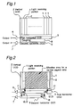
- Fig. 1 is a block diagram of the CCD solid state imaging device of a first embodiment of the present invention. As shown in Fig. 1, this first embodiment device comprises a light receiving portion 1 of an aspect ratio of 16 : 9, a vertical CCD 2, a first horizontal CCD 3, a second horizontal CCD 5, a first output circuit 6, a second output circuit 7, and a coupling 8.
- the light receiving portion 1 generates light receiving portion signal charges in correspondence to incident light, and the vertical CCD 2 in turn transfers the light receiving portion signal charges in the vertical direction.
- the configuration of the light receiving portion 1 and the vertical CCD 2 is of an interline transfer type in this embodiment, but it may be of a frame transfer type.
- the first horizontal CCD 3 has the signal charges transferred thereto from the vertical CCD 2, and transfers the signal charges in the horizontal direction.
- the second horizontal CCD 5, which is arranged in parallel to the first horizontal CCD 3, is coupled with the first horizontal CCD 3 by the coupling 8.
- the coupling 8 can transfer the signal charge, which is being transferred horizontally by the first horizontal CCD 3, to the second horizontal CCD 5 at any time point during the horizontal transfer by the first horizontal CCD 3.
- Wide aspect ratio images with the use of all effective pixels (light-receiving pixels) of the light receiving portion 1 can be obtained by transferring charges from the vertical CCD 2 to the first horizontal CCD 3 and further transferring the charges in the horizontal direction by the first horizontal CCD 3.
- the first horizontal CCD 3 needs to have transferred all the charges transferred thereto from the vertical CCD 2 so as to be empty by the time when it receives the next transfer of charges from the vertical CCD 2. On this account, it is necessary for the first horizontal CCD 3 to be driven at higher speed than the second horizontal CCD 5 or for the first horizontal CCD 3 to drain charges remaining after the transfer of charges to the second horizontal CCD 5.
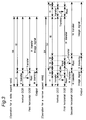
- Fig. 3 is a timing chart of the operation of the first embodiment device.
- signal charges are transferred from the vertical CCD 2 to the first horizontal CCD 3 during a period t1.
- the first horizontal CCD 3 transfers the signal charges in the horizontal direction.
- the second horizontal CCD 5 transfers the signal charges, which have been transferred from the first horizontal CCD 3 during the preceding horizontal period, in the horizontal direction for a complete period from period t1 to period t2.
- the signal charges are transferred from the first horizontal CCD 3 to the second horizontal CCD 5.
- the second horizontal CCD 5 transfers the signal charges in the horizontal direction, so that an image signal is obtained from these signal charges.
- narrow aspect ratio images with the use of any horizontal area of light-receiving pixels can be obtained by making the difference between a timing of charge transfer from the vertical CCD 2 to the first horizontal CCD 3 and that from the first horizontal CCD 3 to the second horizontal CCD 5.
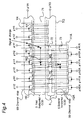
- FIG. 4 A detailed structure of the first horizontal CCD 3, the second horizontal CCD 5 and the coupling 8 is shown in Fig. 4.
- the first horizontal CCD 3 has a channel 71, and horizontal transfer gate electrodes H1, H2.
- the second horizontal CCD 5 has a channel 73, and horizontal transfer gate electrodes H2A, H1A.
- V4 denotes a gate electrode for transferring signal charges from the vertical CCD 2 to the first horizontal CCD 3
- TG denotes a gate electrode for transferring signal charges from the first horizontal CCD 3 to the second horizontal CCD 5.
- Numeral 99 denotes channel stops.
- the channel 71 of the first horizontal CCD 3 is connected to the channel 73 of the second horizontal CCD 5 by a connecting channel 72 between the gate electrode H1 and the gate electrode H1A and under the gate electrode TG.
- the gate electrode TG and the connecting channel 72 make up the coupling 8. Therefore, by changing pulse potentials ⁇ H1, ⁇ H1A, and ⁇ TG to be applied to the gate electrodes TG, H1, and H1A, signal charges can be transferred from under the gate electrode H1 to under the gate electrode H1A. That is, signal charges can be transferred from the first horizontal CCD 3 to the second horizontal CCD 5 via the coupling 8.
- signal charges generated by the light receiving portion 1 are transferred to the first horizontal CCD 3 via the vertical CCD 2, and the signal charges are transferred from the first horizontal CCD 3 to the first output circuit 6, thereby creating an image signal. Consequently, in this case, a wide aspect ratio image can be created by using effective pixels of the entire area of the light receiving portion 1.
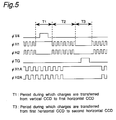
- Fig. 5 is a timing chart of driving pulse signals ⁇ H1 and ⁇ H2, ⁇ H1A and ⁇ H2A, ⁇ V4 and ⁇ TG to be applied to the gate electrodes H1 and H2, H1A and H2A, V4 and TG, respectively, in the case of a narrow aspect ratio of 4 : 3, i.e. in the case where the horizontal dimension of the screen is made smaller than the specified dimension for the aspect ratio of 16 : 9.
- signal charges are transferred from the vertical CCD 2 to the first horizontal CCD 3 through a route W1 as shown in Fig. 4 by a driving pulse signal ⁇ V4 applied to the gate electrode V4.
- the signal charge is transferred in the horizontal direction within the first horizontal CCD 3 as shown by a route W2 by the driving pulse signals ⁇ H1 and ⁇ H2 applied to the gate electrodes H1 and H2, respectively.
- the signal charge under the gate electrode H1 is transferred to under the gate electrode H1A through the connecting channel 72 under the electrode TG, as shown by a route W3, by the driving pulse signal ⁇ TG being applied to the gate electrode TG and the driving pulse signals ⁇ H1 and ⁇ H1A being applied to the gate electrodes H1 and H1A. That is, during the period T3, the signal charge is transferred from the first horizontal CCD 3 to the second horizontal CCD 5 via the coupling 8. Thereafter, the second horizontal CCD 5 transfers the signal charge to the second output circuit 7, and the second output circuit 7 in turn outputs an image signal. Then, the first horizontal CCD 3 further transfers signal charges, sweeping out signal charges of all unwanted pixels unnecessary for a narrow aspect ratio image by the period T1 of the next cycle.
- the present embodiment device is capable of transferring part of the signal charges that are being transferred by the first horizontal CCD 3, to the second horizontal CCD 5 by the coupling 8. Accordingly, by outputting signal charges from the second horizontal CCD 5 to the second output circuit 7, a narrow aspect ratio image formed by pixels of any arbitrary horizontal area out of all the effective pixels of the light receiving portion 1 can be created.
- effective pixels of the light receiving portion can be sufficiently utilized so that there can be obtained an image of a wide aspect ratio of 16 : 9 and another of a narrow aspect ratio of 4 : 3 without using digital signal processing or any optical means.
- Fig. 6 is a block diagram of a second embodiment of the present invention.
- This embodiment device comprises a drain 201 and a connecting channel 203 in addition to the arrangement of the first embodiment as shown in Fig. 1. More specifically, the second embodiment device comprises the connecting channel 203 sandwiched between channel stops 99, 99, the drain 201, and a DC power supply 202 connected between the drain 201 and ground as shown in Fig. 8, in addition to the first embodiment.
- like parts to the first embodiment are designated by like numerals, their description being omitted.
- a first horizontal CCD 3 and the drain 201 are connected to each other by the connecting channel 203 under a gate electrode TG.
- charges can be transferred from the first horizontal CCD 3 to the second horizontal CCD 5.
- unnecessary charges can be discharged from the first horizontal CCD 3 to the drain 201 via the connecting channel 203, and moreover discharged from the drain 201 to the ground.
- the second embodiment device is capable of discharging unnecessary charges via the drain 201, so that the first horizontal CCD 3 and the second horizontal CCD 5 may be driven at the same frequency.
- narrow aspect ratio images can be easily obtained.
- Fig. 9 is a block diagram of a third embodiment of the present invention.
- the third embodiment device comprises a drain 301 and a connecting channel 303, in addition to the arrangement of the first embodiment shown in Fig. 1. More specifically, the third embodiment differs from the first embodiment in that the device comprises the connecting channel 303 sandwiched between channel stops 99, the drain 301, and a DC power supply 302 connected between the drain 301 and ground, as shown in Fig. 11. Accordingly, like parts to the first embodiment are designated by like numerals, their description being omitted.
- a second horizontal CCD 5 and the drain 301 are connected to each other via the connecting channel 303 under a gate electrode TG.
- the drain 301 is connected to the ground via the DC power supply 302. Then by applying a driving signal ⁇ TG2 to the gate electrode TG, charges present in the second horizontal CCD 5 can be discharged to the drain 301 via the connecting channel 303 at any arbitrary time point.
- Fig. 12 is a driving timing chart of each CCD in obtaining a narrow aspect ratio image by the third embodiment.
- the figure shows that, in a horizontal blanking period, during a period t3 preceding a period during which charges are transferred from the first horizontal CCD 3 to the second horizontal CCD 5, unnecessary charges remaining in the second horizontal CCD 5 are discharged via the drain 301.
- the third embodiment is such that after the charges present in the second horizontal CCD 5 have been read at a lower frequency than in the first embodiment, charges remaining in the second horizontal CCD 5 can be discharged via the drain 301.
- the third embodiment it becomes possible to obtain images of any arbitrary aspect ratio narrower than the first embodiment.
- the second embodiment device of Fig. 6 may be further provided with the drain 301 and the connecting channel 303 of the third embodiment of Fig. 9.
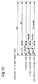
- Fig. 13 is a block diagram of a fourth embodiment of the present invention.
- the device comprises a second horizontal CCD 405 equal in length (number of transfer steps) to the first horizontal CCD 3 and a connecting channel 408 instead of the second horizontal CCD 5 and the connecting channel 8 of the first embodiment shown in Fig. 1, that it also comprises a drain 401 and a connecting channel 403 for discharging part of charges present in the second horizontal CCD 405 at any arbitrary time point, and that it further comprises a drain 404 for discharging charges present in the first horizontal CCD 3 instead of the first output circuit 6 of the third embodiment.
- like parts to the first embodiment are designated by like numerals, their description being omitted, and only the differences from the first embodiment are described below.
- each CCD is operated as shown in Fig. 14 at the driving timing as shown in Fig. 12, and charges are read from the second horizontal CCD 405 at a lower frequency than in the above case for obtaining a wide aspect ratio image. Thereafter, unnecessary charges remaining in the second horizontal CCD 405 are discharged to the drain 401 via the connecting channel 403.
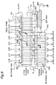
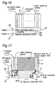
- Fig. 16 is a block diagram of a fifth embodiment of the present invention.
- This embodiment differs from the first embodiment as shown in the block diagram of Fig. 1 in that the device comprises a horizontal optical black portion 29 adjacent to the light receiving portion 1, as well as in the structure of gate electrodes for transferring signal charges in the vertical direction. Therefore, its differences from the first embodiment are mainly described below.
- the fifth embodiment device comprises a horizontal optical black portion 29 adjacent to the light receiving portion 1.
- the horizontal optical black portion 29 generates horizontal optical black signal charges.
- horizontal optical black signal charges generated by the horizontal optical black portion 29 can be transferred from a vertical CCD 2 to the second horizontal CCD 25 via the first horizontal CCD 23 without being mixed with the charges that are being transferred by the first horizontal CCD 23, that is, independently of the charges generated by the light receiving portion 1.
- first horizontal CCD 23 and a second horizontal CCD 25 of the fifth embodiment Detailed structure of a first horizontal CCD 23 and a second horizontal CCD 25 of the fifth embodiment is shown in Fig. 18.
- first horizontal CCD 23 has a channel 91, and horizontal transfer gate electrodes H1, H2.
- second horizontal CCD 25 has a channel 93 and horizontal transfer gate electrodes H1A, H2A.
- the channel 91 of the first horizontal CCD 23 and the channel 93 of the second horizontal CCD 25 are connected to each other by a connecting channel 92 located between the gate electrodes H1 and H1A and under gate electrodes TG4 and TG3.
- a larger-width portion V4a of a gate electrode V4 functions to transfer light receiving portion signal charges generated by the light receiving portion 1 to the first horizontal CCD 23 via the vertical CCD 2.
- a smaller-width portion V4b of the gate electrode V4 and gate electrodes TG1 and TG2 function to transfer horizontal optical black signal charges generated by the horizontal optical black portion 29 to the channel 91 of the first horizontal CCD 23.
- the gate electrode TG4 functions to transfer the horizontal optical black signal charges from the first horizontal CCD 23 to the second horizontal CCD 25.
- the gate electrode TG3 functions to transfer the light receiving portion signal charges from the first horizontal CCD 23 to the second horizontal CCD 25.
- the connecting channel 92, and the gate electrodes TG3 and TG4 make up a coupling 28.
- the fifth embodiment device is so arranged that a portion of the vertical CCD 2 corresponding to the horizontal optical black portion 29 and the first horizontal CCD 23 are connected to each other via two gate electrodes TG1 and TG2, thereby allowing signal charges generated by the horizontal optical black portion 29 and charges generated by the light receiving portion 1 to be transferred independently of each other.
- the potential of the connecting channel 92 under the gate electrode TG4 is made deeper than that of the channel 91. Also, a potential difference is provided by ion implantation between a part of the channel 91 under the gate electrode H1 and a part of the channel 91 under the gate electrode H2.
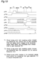
- Fig. 19 there is shown a timing chart of driving pulse signals ⁇ H1 and ⁇ H2, ⁇ H1A and ⁇ H2A, ⁇ V4 and ⁇ TG1 to ⁇ TG4 to be applied to the gate electrodes H1 and H2, H1A and H2A, V4 and TG1 to TG4 in the case of a narrow aspect ratio.
- signal charges generated by the light receiving portion 1 are transferred from the vertical CCD 2 to the channel 91 of the first horizontal CCD 23, as shown by routes Y1 and Z1 in Fig. 18, by a driving pulse signal ⁇ V4 applied to the gate electrode V4.
- horizontal optical black signal charges generated by the horizontal optical black portion 29 are transferred to and accumulated under the gate electrode TG1 via the smaller-width portion V4b of the gate electrode V4, as shown by a route X1 in Fig. 18.
- light receiving portion signal charges are transferred in the horizontal direction within the first horizontal CCD 23, as shown by routes Y2 and Z2 in Fig. 18, by driving pulse signals ⁇ H1 and ⁇ H2 applied to the gate electrodes H1 and H2 of the first horizontal CCD 23.
- a driving pulse signal is applied to the gate electrode TG3.
- the signal charges transferred to under the gate electrode H1 of the first horizontal CCD 23 via the routes Z1 and Z2 are transferred to under the gate electrode H1A of the second horizontal CCD 25 through a route Z3, i.e. through under the gate electrode TG3 of the coupling 28.
- the above horizontal optical black signal charges and the above light receiving portion signal charges are serially transferred from the second horizontal CCD 25 to an output circuit 27. Also, unnecessary light receiving portion signal charges are swept out from the first horizontal CCD 23.
- horizontal optical black signal charges generated by the horizontal optical black portion 29 can be transferred from the vertical CCD 2 to the second horizontal CCD 25 via the first horizontal CCD 23 without being mixed with charges that are being transferred by the first horizontal CCD 23, independently of charges generated by the light receiving portion 1.
- horizontal optical black signals can be utilized not only to create a wide aspect ratio image by charges transferred by the first horizontal CCD 23 but also to create a narrow aspect ratio image by charges transferred by the second horizontal CCD 25.
- the second, third and fourth embodiment devices may be further provided with the horizontal optical black portion 29, the smaller-width portion V4b of the gate electrode V4, and the gate electrodes TG1, TG2, TG4 of the fifth embodiment device.
- Fig. 20 is a block diagram of a sixth embodiment of the present invention.
- the sixth embodiment device comprises a light receiving portion 31, a vertical CCD 32, a first horizontal CCD 33, a second horizontal CCD 35, a coupling 38, a coupling CCD 110, a first drain 36, a second drain 37, and an output circuit 39.
- the sixth embodiment differs from the first embodiment of the invention shown in Fig. 1 only in that the device has the first and second horizontal CCDs each provided with a drain and connected at their forward ends in the direction of charge transfer and that it has a single output circuit. Thus, these differences are mainly described below.
- the first horizontal CCD 33 and the second horizontal CCD 35 are coupled with each other at their forward ends in the direction of charge transfer by a coupling CCD 110. Also, the first horizontal CCD 33 and the second horizontal CCD 35 are provided with a first drain 36 and a second drain 37, respectively, for discharging unnecessary charges. Further, this embodiment device has an output circuit 39, to which signal charges are transferred from the coupling CCD 110.
- Fig. 21 Detailed structure in the vicinity of the coupling CCD 110 that couples the first horizontal CCD 33 and the second horizontal CCD 35 with each other is shown in Fig. 21.
- a channel 111 of the first horizontal CCD 33 and a channel 112 of the second horizontal CCD 35 are coupled with each other by a channel 113 of the coupling CCD 110.
- the coupling CCD 110 has gate electrodes H1B and H2B of such a configuration as if the gate electrodes H1 and H2 of the first horizontal CCD 33 and the gate electrodes H1A and H2A of the second horizontal CCD 35 were coupled together.
- the gate electrodes H1B and H2B of the coupling CCD 110 are to be driven by gate clock signals ⁇ H1B and ⁇ H2B that are generated by the same clock as the one by which driving pulse signals ⁇ H1, ⁇ H2, ⁇ H1A, and ⁇ H2A applied to the gate electrodes H1, H2, H1A, and H2A of the first and second horizontal CCDs 33 and 35 are generated.
- a gate electrode D1, a gate electrode CG1, and a channel 115 sandwiched by the gate electrodes D1 and CG1 make up the first drain 36.
- a gate electrode D2, a gate electrode CG2, and a channel 116 sandwiched by the gate electrodes D2 and CG2 make up the second drain 37.
- unnecessary signal charges and dark-current charges that are present in the channel 111 of the first horizontal CCD 33 can be discharged from the first drain 36.
- unnecessary signal charges and dark-current charges that are present in the channel 112 of the second horizontal CCD 35 can be discharged from the second drain 37.
- one output circuit 39 connected to the coupling CCD 110 can be shared between the first horizontal CCD 33 and the second horizontal CCD 35.
- the second, third, and fifth embodiment devices may be further provided with the first and second drains 36 and 37, and the coupling CCD 110 of the sixth embodiment device.
Landscapes
- Engineering & Computer Science (AREA)
- Multimedia (AREA)
- Signal Processing (AREA)
- Transforming Light Signals Into Electric Signals (AREA)
- Solid State Image Pick-Up Elements (AREA)
Claims (7)
- Dispositif de formation d'image à semi-conducteur de type CCD, comprenant:une partie de réception de lumière (1, 31) pour recevoir des lumières et produire des charges correspondant aux lumières;un dispositif CCD vertical (2, 32) pour transférer les charges provenant de la partie de réception de lumière (1, 31) dans une direction verticale;un premier dispositif CCD horizontal (3, 23, 33) pour recevoir les charges provenant du dispositif CCD vertical (2, 32) et transférer les charges dans une direction horizontale;un second dispositif CCD horizontal (5, 405, 25, 35) qui est disposé parallèlement au premier dispositif CCD horizontal (3, 33) et transfère les charges reçues du premier dispositif CCD horizontal (3, 33) dans la direction horizontale; etun couplage de transfert de charges (8, 38) entre les premier et second dispositifs CCD horizontaux,caractérisé par des moyens pour fournir auxdits premier et second dispositifs CCD horizontaux et audit couplage des signaux de commande qui commandent le fonctionnement du dispositif de telle manière que les charges, qui sont transférées dans la direction horizontale par le premier dispositif CCD horizontal (3, 23, 33), sont transférées au second dispositif CCD horizontal (5, 405, 25, 35) à un instant arbitraire quelconque pendant un transfert horizontal par le premier dispositif CCD horizontal (3, 23, 33).
- Dispositif de formation d'image à semi-conducteur de type CCD selon la revendication 1, comprenant également:des moyens de décharge de charges (201, 404) pour décharger au moins une partie des charges présentes dans le premier dispositif CCD horizontal (3) à un instant arbitraire quelconque.
- Dispositif de formation d'image à semi-conducteur de type CCD selon la revendication 1 ou 2, comprenant également:des moyens de décharge de charges (301, 401) pour décharger au moins une partie des charges présentes dans le second dispositif CCD horizontal (5, 405) à un instant arbitraire quelconque.
- Dispositif de formation d'image à semi-conducteur de type CCD selon la revendication 3,dans lequel le second dispositif CCD horizontal (405) a une capacité de transfert de charges lui permettant de transférer toutes les charges transférées depuis le dispositif CCD vertical (2).
- Dispositif de formation d'image à semi-conducteur de type CCD selon l'une quelconque des revendications précédentes, comprenant également:une partie noire optique horizontale (29) adjacente à la partie de réception de lumière (1);des premiers moyens d'électrode de grille (V4b, TG1, TG2) pour transférer des charges de signal de noir optique horizontal produites par la partie noire optique horizontale (29) vers le premier dispositif CCD horizontal (23); etdes seconds moyens d'électrode de grille (TG4) pour transférer les charges de signal de noir optique horizontal du premier dispositif CCD horizontal (23) vers le second dispositif CCD horizontal (25).
- Dispositif de formation d'image à semi-conducteur de type CCD selon la revendication 1, la revendication 2, la revendication 3 lorsqu'elle dépend de la revendication 2 ou la revendication 5 lorsqu'elle dépend de la revendication 1, comprenant également:un premier drain (36) pour décharger des charges présentes dans le premier dispositif CCD horizontal (33);un second drain (37) pour décharger des charges présentes dans le second dispositif CCD horizontal (35); etun couplage CCD (110) pour coupler le premier dispositif CCD horizontal (33) et le second dispositif CCD horizontal (35) à leurs extrémités à proximité d'un circuit de sortie de charges (39).
- Procédé pour faire fonctionner un dispositif de formation d'image à semi-conducteur de type CCD, le dispositif comprenant:une partie de réception de lumière (1, 31) pour recevoir des lumières et produire des charges correspondant aux lumières;un dispositif CCD vertical (2, 32) pour transférer les charges provenant de la partie de réception de lumière (1, 31) dans une direction verticale;un premier dispositif CCD horizontal (3, 23, 33) pour recevoir les charges provenant du dispositif CCD vertical (2, 32) et transférer les charges dans une direction horizontale;un second dispositif CCD horizontal (5, 405, 25, 35) qui est disposé parallèlement au premier dispositif CCD horizontal (3, 33) et transfère les charges reçues du premier dispositif CCD horizontal (3, 33) dans la direction horizontale; etun couplage de transfert de charges (8, 38) entre les premier et second dispositifs CCD horizontaux,le procédé étant caractérisé par les étapes consistant à faire fonctionner ledit couplage de façon à transférer les charges, qui sont transférées dans la direction horizontale par le premier dispositif CCD horizontal (3, 23, 33), au second dispositif CCD horizontal (5, 405, 25, 35) à un instant arbitraire pendant un transfert horizontal par le premier dispositif CCD horizontal (3, 23, 33).
Applications Claiming Priority (6)
| Application Number | Priority Date | Filing Date | Title |
|---|---|---|---|
| JP29692092 | 1992-11-06 | ||
| JP29692092 | 1992-11-06 | ||
| JP296920/92 | 1992-11-06 | ||
| JP25413193 | 1993-10-12 | ||
| JP254131/93 | 1993-10-12 | ||
| JP5254131A JPH06205298A (ja) | 1992-11-06 | 1993-10-12 | 電荷結合型固体撮像装置 |
Publications (3)
| Publication Number | Publication Date |
|---|---|
| EP0596748A2 EP0596748A2 (fr) | 1994-05-11 |
| EP0596748A3 EP0596748A3 (fr) | 1994-12-07 |
| EP0596748B1 true EP0596748B1 (fr) | 2000-02-09 |
Family
ID=26541550
Family Applications (1)
| Application Number | Title | Priority Date | Filing Date |
|---|---|---|---|
| EP93308861A Expired - Lifetime EP0596748B1 (fr) | 1992-11-06 | 1993-11-05 | Capteur d'image à CCD la génération d'une pluralité de formats d'image, utilisant efficacement la surface photosensible |
Country Status (5)
| Country | Link |
|---|---|
| US (1) | US5486859A (fr) |
| EP (1) | EP0596748B1 (fr) |
| JP (1) | JPH06205298A (fr) |
| KR (1) | KR940013159A (fr) |
| DE (1) | DE69327828T2 (fr) |
Families Citing this family (29)
| Publication number | Priority date | Publication date | Assignee | Title |
|---|---|---|---|---|
| BE1008077A3 (nl) * | 1994-02-17 | 1996-01-09 | Philips Electronics Nv | Ladingsgekoppelde beeldopneeminrichting en camera voorzien van een dergelijke ladingsgekoppelde beeldopneeminrichting. |
| US6721009B1 (en) * | 1994-11-12 | 2004-04-13 | Sony Corporation | Method of driving solid state imaging device |
| JP4030605B2 (ja) * | 1995-11-10 | 2008-01-09 | オリンパス株式会社 | 電子的撮像装置 |
| US5854656A (en) * | 1995-11-15 | 1998-12-29 | Logitech, Inc. | Non-uniform clocking system for area imaging device |
| US5798786A (en) * | 1996-05-07 | 1998-08-25 | Recon/Optical, Inc. | Electro-optical imaging detector array for a moving vehicle which includes two axis image motion compensation and transfers pixels in row directions and column directions |
| US5844602A (en) * | 1996-05-07 | 1998-12-01 | Recon/Optical, Inc. | Electro-optical imaging array and camera system with pitch rate image motion compensation which can be used in an airplane in a dive bomb maneuver |
| JP4329128B2 (ja) * | 1996-07-12 | 2009-09-09 | ソニー株式会社 | 固体撮像装置、固体撮像装置の駆動方法およびカメラ |
| JP4084857B2 (ja) * | 1996-08-30 | 2008-04-30 | 本田技研工業株式会社 | 自動車の前方監視システムにおけるイメージセンサの縦横比設定方法 |
| KR100226787B1 (en) * | 1996-12-16 | 1999-10-15 | Hyundai Micro Electronics Co | Ccd device |
| JPH11112885A (ja) * | 1997-10-03 | 1999-04-23 | Olympus Optical Co Ltd | カメラ |
| US6707498B1 (en) * | 1997-11-11 | 2004-03-16 | Fuji Photo Film Co., Ltd. | Charge transfer of solid-state image pickup device |
| JP3548410B2 (ja) * | 1997-12-25 | 2004-07-28 | キヤノン株式会社 | 固体撮像装置および固体撮像装置の信号読み出し方法 |
| JPH11196332A (ja) * | 1997-12-26 | 1999-07-21 | Canon Inc | 固体撮像装置 |
| JP3592147B2 (ja) * | 1998-08-20 | 2004-11-24 | キヤノン株式会社 | 固体撮像装置 |
| JP3700488B2 (ja) * | 1999-09-06 | 2005-09-28 | 日本ビクター株式会社 | 広角画像撮像装置 |
| JP3922853B2 (ja) * | 1999-12-07 | 2007-05-30 | 松下電器産業株式会社 | 固体撮像装置 |
| US6803960B2 (en) * | 1999-12-22 | 2004-10-12 | Eastman Kodak Company | Optical test structure for measuring charge-transfer efficiency |
| US6507056B1 (en) * | 2000-03-22 | 2003-01-14 | Eastman Kodak Company | Fast line dump structure for solid state image sensor |
| JP2002176581A (ja) * | 2000-12-05 | 2002-06-21 | Funai Electric Co Ltd | 電子写真装置 |
| JP2002344982A (ja) * | 2001-05-18 | 2002-11-29 | Sanyo Electric Co Ltd | 固体撮像素子及びその駆動方法 |
| JP3956719B2 (ja) | 2002-02-26 | 2007-08-08 | 日本ビクター株式会社 | 撮像装置 |
| US20050062868A1 (en) * | 2003-03-24 | 2005-03-24 | Tomohiro Shiiba | Solid-state imaging device and method of driving solid-state imaging device |
| US20050258249A1 (en) * | 2004-04-29 | 2005-11-24 | Giebel James R | Imaging pixel array with programmable pixel aspect ratio for an optical code reader |
| JP4630200B2 (ja) * | 2005-03-07 | 2011-02-09 | 富士フイルム株式会社 | 固体撮像素子および撮像装置 |
| JP4333664B2 (ja) * | 2005-11-11 | 2009-09-16 | ソニー株式会社 | 固体撮像素子及び固体撮像装置 |
| JP2007201160A (ja) * | 2006-01-26 | 2007-08-09 | Fujifilm Corp | 電荷結合素子 |
| JP4740781B2 (ja) * | 2006-03-30 | 2011-08-03 | 富士フイルム株式会社 | 固体撮像装置 |
| US7692706B2 (en) * | 2006-07-20 | 2010-04-06 | Eastman Kodak Company | Charge summing in multiple output charge-coupled devices in an image sensor |
| JP2012049911A (ja) * | 2010-08-27 | 2012-03-08 | Canon Inc | 光電変換装置および撮像システム |
Family Cites Families (9)
| Publication number | Priority date | Publication date | Assignee | Title |
|---|---|---|---|---|
| JPS58190170A (ja) * | 1982-04-30 | 1983-11-07 | Toshiba Corp | 固体撮像装置 |
| JPS63109684A (ja) * | 1986-10-27 | 1988-05-14 | Nec Home Electronics Ltd | 撮像装置 |
| US4819070A (en) * | 1987-04-10 | 1989-04-04 | Texas Instruments Incorporated | Image sensor array |
| US4995061A (en) * | 1987-12-17 | 1991-02-19 | Texas Instruments Incorporated | Two-phase CCD imager cell for TV interlace operation |
| JP2730031B2 (ja) * | 1988-01-22 | 1998-03-25 | ソニー株式会社 | 固体撮像素子の駆動回路 |
| US4980771A (en) * | 1988-02-18 | 1990-12-25 | Victor Company Of Japan, Ltd. | Imaging device and imaging apparatus including the imaging device |
| JPH0234089A (ja) * | 1988-07-25 | 1990-02-05 | Fuji Photo Optical Co Ltd | アスペクト比調整機能付画像入力装置 |
| JPH03198486A (ja) * | 1989-12-26 | 1991-08-29 | Sony Corp | 撮像装置 |
| JPH0477510A (ja) * | 1990-07-16 | 1992-03-11 | Asahi Chem Ind Co Ltd | 制振性に優れた耐衝撃性スチレン系樹脂組成物 |
-
1993
- 1993-10-12 JP JP5254131A patent/JPH06205298A/ja active Pending
- 1993-11-03 US US08/147,850 patent/US5486859A/en not_active Expired - Lifetime
- 1993-11-05 KR KR1019930023447A patent/KR940013159A/ko not_active Ceased
- 1993-11-05 EP EP93308861A patent/EP0596748B1/fr not_active Expired - Lifetime
- 1993-11-05 DE DE69327828T patent/DE69327828T2/de not_active Expired - Fee Related
Also Published As
| Publication number | Publication date |
|---|---|
| KR940013159A (ko) | 1994-06-25 |
| DE69327828D1 (de) | 2000-03-16 |
| US5486859A (en) | 1996-01-23 |
| JPH06205298A (ja) | 1994-07-22 |
| EP0596748A2 (fr) | 1994-05-11 |
| DE69327828T2 (de) | 2000-06-15 |
| EP0596748A3 (fr) | 1994-12-07 |
Similar Documents
| Publication | Publication Date | Title |
|---|---|---|
| EP0596748B1 (fr) | Capteur d'image à CCD la génération d'une pluralité de formats d'image, utilisant efficacement la surface photosensible | |
| US4831453A (en) | Solid-state imaging device having high-speed shutter function and method of realizing high-speed function in solid-state imaging device | |
| US6452634B1 (en) | Charge transfer device and method of driving the same, and solid state imaging device and method of driving the same | |
| EP0757496B1 (fr) | Capteur d'images en couleurs | |
| JP3906496B2 (ja) | 固体撮像装置およびその駆動方法、並びにカメラ | |
| JPH08331461A (ja) | 固体撮像装置の駆動方法 | |
| NL8201745A (nl) | Beeldopneeminrichting van het "solid state"-type. | |
| JP4320835B2 (ja) | 固体撮像装置およびその駆動方法並びにカメラシステム | |
| KR100317570B1 (ko) | 고체 촬상 장치의 구동 방법 | |
| JPH04262679A (ja) | 固体撮像素子の駆動方法 | |
| EP0498662B1 (fr) | Une méthode pour la lecture de signaux issus d'un dispositif de prise d'image à l'état solide | |
| EP0720387A2 (fr) | Méthode et appareil pour générer des images entrelacées à partir d'un capteur d'image à balayage progressif dans une caméra électronique | |
| JPH07221922A (ja) | 撮像装置 | |
| US8045025B2 (en) | Image pickup device adaptable to display fewer vertical pixels | |
| US7492403B2 (en) | Solid state image sensing device and driving method with sub-sampling mode and improved dynamic range | |
| JP2000138943A (ja) | 固体撮像素子およびその駆動方法並びにカメラシステム | |
| US7245323B2 (en) | Transferring method of electric charge from image sensing device and the image sensing device | |
| KR100417215B1 (ko) | Ccd 고체촬상소자의 구동방법 | |
| KR20080035505A (ko) | 고체 촬상 장치 및 그 구동 방법, 전자 정보 기기 | |
| JP2966740B2 (ja) | 固体撮像素子及びその駆動方法 | |
| JP3392607B2 (ja) | 固体撮像素子の駆動方法 | |
| JP3707910B2 (ja) | 固体撮像素子およびその駆動方法 | |
| JPH09312849A (ja) | 固体撮像装置 | |
| KR19990067776A (ko) | 고체 촬상 장치 및 그 구동 방법 | |
| JPH0918888A (ja) | リニアセンサカメラを用いた撮像装置 |
Legal Events
| Date | Code | Title | Description |
|---|---|---|---|
| PUAI | Public reference made under article 153(3) epc to a published international application that has entered the european phase |
Free format text: ORIGINAL CODE: 0009012 |
|
| AK | Designated contracting states |
Kind code of ref document: A2 Designated state(s): DE FR GB NL |
|
| PUAL | Search report despatched |
Free format text: ORIGINAL CODE: 0009013 |
|
| AK | Designated contracting states |
Kind code of ref document: A3 Designated state(s): DE FR GB NL |
|
| 17P | Request for examination filed |
Effective date: 19950309 |
|
| 17Q | First examination report despatched |
Effective date: 19970131 |
|
| GRAG | Despatch of communication of intention to grant |
Free format text: ORIGINAL CODE: EPIDOS AGRA |
|
| GRAG | Despatch of communication of intention to grant |
Free format text: ORIGINAL CODE: EPIDOS AGRA |
|
| GRAG | Despatch of communication of intention to grant |
Free format text: ORIGINAL CODE: EPIDOS AGRA |
|
| GRAH | Despatch of communication of intention to grant a patent |
Free format text: ORIGINAL CODE: EPIDOS IGRA |
|
| GRAH | Despatch of communication of intention to grant a patent |
Free format text: ORIGINAL CODE: EPIDOS IGRA |
|
| GRAA | (expected) grant |
Free format text: ORIGINAL CODE: 0009210 |
|
| AK | Designated contracting states |
Kind code of ref document: B1 Designated state(s): DE FR GB NL |
|
| REF | Corresponds to: |
Ref document number: 69327828 Country of ref document: DE Date of ref document: 20000316 |
|
| ET | Fr: translation filed | ||
| PLBE | No opposition filed within time limit |
Free format text: ORIGINAL CODE: 0009261 |
|
| 26N | No opposition filed | ||
| REG | Reference to a national code |
Ref country code: GB Ref legal event code: IF02 |
|
| PGFP | Annual fee paid to national office [announced via postgrant information from national office to epo] |
Ref country code: NL Payment date: 20071115 Year of fee payment: 15 Ref country code: DE Payment date: 20071101 Year of fee payment: 15 |
|
| PGFP | Annual fee paid to national office [announced via postgrant information from national office to epo] |
Ref country code: GB Payment date: 20071031 Year of fee payment: 15 Ref country code: FR Payment date: 20071108 Year of fee payment: 15 |
|
| GBPC | Gb: european patent ceased through non-payment of renewal fee |
Effective date: 20081105 |
|
| PG25 | Lapsed in a contracting state [announced via postgrant information from national office to epo] |
Ref country code: NL Free format text: LAPSE BECAUSE OF NON-PAYMENT OF DUE FEES Effective date: 20090601 |
|
| NLV4 | Nl: lapsed or anulled due to non-payment of the annual fee |
Effective date: 20090601 |
|
| REG | Reference to a national code |
Ref country code: FR Ref legal event code: ST Effective date: 20090731 |
|
| PG25 | Lapsed in a contracting state [announced via postgrant information from national office to epo] |
Ref country code: DE Free format text: LAPSE BECAUSE OF NON-PAYMENT OF DUE FEES Effective date: 20090603 |
|
| PG25 | Lapsed in a contracting state [announced via postgrant information from national office to epo] |
Ref country code: GB Free format text: LAPSE BECAUSE OF NON-PAYMENT OF DUE FEES Effective date: 20081105 |
|
| PG25 | Lapsed in a contracting state [announced via postgrant information from national office to epo] |
Ref country code: FR Free format text: LAPSE BECAUSE OF NON-PAYMENT OF DUE FEES Effective date: 20081130 |