EP0597497A1 - Circuit d'adaptation d'accord électronique utilisant des éléments d'inductance ajustables et circuits oscillants - Google Patents
Circuit d'adaptation d'accord électronique utilisant des éléments d'inductance ajustables et circuits oscillants Download PDFInfo
- Publication number
- EP0597497A1 EP0597497A1 EP93118387A EP93118387A EP0597497A1 EP 0597497 A1 EP0597497 A1 EP 0597497A1 EP 93118387 A EP93118387 A EP 93118387A EP 93118387 A EP93118387 A EP 93118387A EP 0597497 A1 EP0597497 A1 EP 0597497A1
- Authority
- EP
- European Patent Office
- Prior art keywords
- impedance
- terminal
- tank circuit
- capacitor
- variable inductance
- Prior art date
- Legal status (The legal status is an assumption and is not a legal conclusion. Google has not performed a legal analysis and makes no representation as to the accuracy of the status listed.)
- Withdrawn
Links
Images


Classifications
-
- H—ELECTRICITY
- H01—ELECTRIC ELEMENTS
- H01J—ELECTRIC DISCHARGE TUBES OR DISCHARGE LAMPS
- H01J37/00—Discharge tubes with provision for introducing objects or material to be exposed to the discharge, e.g. for the purpose of examination or processing thereof
- H01J37/32—Gas-filled discharge tubes
- H01J37/32009—Arrangements for generation of plasma specially adapted for examination or treatment of objects, e.g. plasma sources
- H01J37/32082—Radio frequency generated discharge
- H01J37/32174—Circuits specially adapted for controlling the RF discharge
- H01J37/32183—Matching circuits
-
- H—ELECTRICITY
- H01—ELECTRIC ELEMENTS
- H01F—MAGNETS; INDUCTANCES; TRANSFORMERS; SELECTION OF MATERIALS FOR THEIR MAGNETIC PROPERTIES
- H01F29/00—Variable transformers or inductances not covered by group H01F21/00
- H01F29/14—Variable transformers or inductances not covered by group H01F21/00 with variable magnetic bias
- H01F29/146—Constructional details
-
- H—ELECTRICITY
- H01—ELECTRIC ELEMENTS
- H01J—ELECTRIC DISCHARGE TUBES OR DISCHARGE LAMPS
- H01J37/00—Discharge tubes with provision for introducing objects or material to be exposed to the discharge, e.g. for the purpose of examination or processing thereof
- H01J37/32—Gas-filled discharge tubes
- H01J37/32009—Arrangements for generation of plasma specially adapted for examination or treatment of objects, e.g. plasma sources
- H01J37/32082—Radio frequency generated discharge
-
- H—ELECTRICITY
- H01—ELECTRIC ELEMENTS
- H01J—ELECTRIC DISCHARGE TUBES OR DISCHARGE LAMPS
- H01J37/00—Discharge tubes with provision for introducing objects or material to be exposed to the discharge, e.g. for the purpose of examination or processing thereof
- H01J37/32—Gas-filled discharge tubes
- H01J37/32009—Arrangements for generation of plasma specially adapted for examination or treatment of objects, e.g. plasma sources
- H01J37/32082—Radio frequency generated discharge
- H01J37/321—Radio frequency generated discharge the radio frequency energy being inductively coupled to the plasma
-
- H—ELECTRICITY
- H01—ELECTRIC ELEMENTS
- H01J—ELECTRIC DISCHARGE TUBES OR DISCHARGE LAMPS
- H01J37/00—Discharge tubes with provision for introducing objects or material to be exposed to the discharge, e.g. for the purpose of examination or processing thereof
- H01J37/32—Gas-filled discharge tubes
- H01J37/32009—Arrangements for generation of plasma specially adapted for examination or treatment of objects, e.g. plasma sources
- H01J37/32082—Radio frequency generated discharge
- H01J37/32137—Radio frequency generated discharge controlling of the discharge by modulation of energy
- H01J37/32146—Amplitude modulation, includes pulsing
-
- H—ELECTRICITY
- H01—ELECTRIC ELEMENTS
- H01J—ELECTRIC DISCHARGE TUBES OR DISCHARGE LAMPS
- H01J37/00—Discharge tubes with provision for introducing objects or material to be exposed to the discharge, e.g. for the purpose of examination or processing thereof
- H01J37/32—Gas-filled discharge tubes
- H01J37/32009—Arrangements for generation of plasma specially adapted for examination or treatment of objects, e.g. plasma sources
- H01J37/32082—Radio frequency generated discharge
- H01J37/32137—Radio frequency generated discharge controlling of the discharge by modulation of energy
- H01J37/32155—Frequency modulation
- H01J37/32165—Plural frequencies
-
- H—ELECTRICITY
- H01—ELECTRIC ELEMENTS
- H01J—ELECTRIC DISCHARGE TUBES OR DISCHARGE LAMPS
- H01J37/00—Discharge tubes with provision for introducing objects or material to be exposed to the discharge, e.g. for the purpose of examination or processing thereof
- H01J37/32—Gas-filled discharge tubes
- H01J37/32431—Constructional details of the reactor
- H01J37/32458—Vessel
-
- H—ELECTRICITY
- H01—ELECTRIC ELEMENTS
- H01J—ELECTRIC DISCHARGE TUBES OR DISCHARGE LAMPS
- H01J37/00—Discharge tubes with provision for introducing objects or material to be exposed to the discharge, e.g. for the purpose of examination or processing thereof
- H01J37/32—Gas-filled discharge tubes
- H01J37/32431—Constructional details of the reactor
- H01J37/32458—Vessel
- H01J37/32522—Temperature
-
- H—ELECTRICITY
- H01—ELECTRIC ELEMENTS
- H01J—ELECTRIC DISCHARGE TUBES OR DISCHARGE LAMPS
- H01J37/00—Discharge tubes with provision for introducing objects or material to be exposed to the discharge, e.g. for the purpose of examination or processing thereof
- H01J37/32—Gas-filled discharge tubes
- H01J37/32431—Constructional details of the reactor
- H01J37/3266—Magnetic control means
- H01J37/32688—Multi-cusp fields
-
- H—ELECTRICITY
- H01—ELECTRIC ELEMENTS
- H01J—ELECTRIC DISCHARGE TUBES OR DISCHARGE LAMPS
- H01J37/00—Discharge tubes with provision for introducing objects or material to be exposed to the discharge, e.g. for the purpose of examination or processing thereof
- H01J37/32—Gas-filled discharge tubes
- H01J37/32431—Constructional details of the reactor
- H01J37/32697—Electrostatic control
- H01J37/32706—Polarising the substrate
-
- H—ELECTRICITY
- H01—ELECTRIC ELEMENTS
- H01J—ELECTRIC DISCHARGE TUBES OR DISCHARGE LAMPS
- H01J37/00—Discharge tubes with provision for introducing objects or material to be exposed to the discharge, e.g. for the purpose of examination or processing thereof
- H01J37/32—Gas-filled discharge tubes
- H01J37/32431—Constructional details of the reactor
- H01J37/32798—Further details of plasma apparatus not provided for in groups H01J37/3244 - H01J37/32788; special provisions for cleaning or maintenance of the apparatus
- H01J37/32853—Hygiene
- H01J37/32871—Means for trapping or directing unwanted particles
-
- H—ELECTRICITY
- H03—ELECTRONIC CIRCUITRY
- H03H—IMPEDANCE NETWORKS, e.g. RESONANT CIRCUITS; RESONATORS
- H03H11/00—Networks using active elements
- H03H11/02—Multiple-port networks
- H03H11/28—Impedance matching networks
- H03H11/30—Automatic matching of source impedance to load impedance
-
- H—ELECTRICITY
- H03—ELECTRONIC CIRCUITRY
- H03H—IMPEDANCE NETWORKS, e.g. RESONANT CIRCUITS; RESONATORS
- H03H7/00—Multiple-port networks comprising only passive electrical elements as network components
- H03H7/38—Impedance-matching networks
- H03H7/40—Automatic matching of load impedance to source impedance
-
- H—ELECTRICITY
- H05—ELECTRIC TECHNIQUES NOT OTHERWISE PROVIDED FOR
- H05H—PLASMA TECHNIQUE; PRODUCTION OF ACCELERATED ELECTRICALLY-CHARGED PARTICLES OR OF NEUTRONS; PRODUCTION OR ACCELERATION OF NEUTRAL MOLECULAR OR ATOMIC BEAMS
- H05H1/00—Generating plasma; Handling plasma
- H05H1/24—Generating plasma
- H05H1/46—Generating plasma using applied electromagnetic fields, e.g. high frequency or microwave energy
-
- H—ELECTRICITY
- H10—SEMICONDUCTOR DEVICES; ELECTRIC SOLID-STATE DEVICES NOT OTHERWISE PROVIDED FOR
- H10P—GENERIC PROCESSES OR APPARATUS FOR THE MANUFACTURE OR TREATMENT OF DEVICES COVERED BY CLASS H10
- H10P50/00—Etching of wafers, substrates or parts of devices
- H10P50/20—Dry etching; Plasma etching; Reactive-ion etching
- H10P50/28—Dry etching; Plasma etching; Reactive-ion etching of insulating materials
- H10P50/282—Dry etching; Plasma etching; Reactive-ion etching of insulating materials of inorganic materials
- H10P50/283—Dry etching; Plasma etching; Reactive-ion etching of insulating materials of inorganic materials by chemical means
-
- H—ELECTRICITY
- H01—ELECTRIC ELEMENTS
- H01F—MAGNETS; INDUCTANCES; TRANSFORMERS; SELECTION OF MATERIALS FOR THEIR MAGNETIC PROPERTIES
- H01F29/00—Variable transformers or inductances not covered by group H01F21/00
- H01F29/14—Variable transformers or inductances not covered by group H01F21/00 with variable magnetic bias
- H01F2029/143—Variable transformers or inductances not covered by group H01F21/00 with variable magnetic bias with control winding for generating magnetic bias
Definitions
- This invention relates generally to impedance matching networks for matching a source impedance with a load impedance.
- a common goal in connecting a source of electrical power to an electrical load is to maximize the power transfer from the source to the load. This goal is met when the output impedance of the source, or generator, is equal to the complex conjugate of the input impedance of the load.
- impedance in alternating current (ac) circuits, impedance has a resistive component, referred to as the real component, and an inductive or capacitive component, referred to as the imaginary component.
- a simple resistive impedance may be thought of as a vector with a phase angle of zero.
- a complex impedance has a magnitude and a phase angle. Impedances that are complex conjugates of each other have equal magnitudes, but phase angles of equal magnitude and opposite sign.
- the source or generator impedance does not match the load impedance, and an impedance matching network may be connected between the source and the load.
- the function of the impedance matching network is to present to the generator an impedance equal to the complex conjugate of the generator impedance, and to present to the load an impedance equal to the complex conjugate of the load impedance.
- the matching network contains a number of interconnected inductors and capacitors, some of which are adjustable in value to achieve the desired result.
- U.S. Patents 2,611,030, 4,375,051 and 4,621,242 disclose impedance matching circuits which use variable capacitance elements or a multi-tap transformer to adjust the impedance of matching circuits.
- the variable elements are adjusted by motors or solenoids.
- a disadvantage of these designs is that the adjustable elements are not solid state, and therefore will have reliability problems and a relatively slow response time.
- U.S. Patents 2,884,632 and 4,951,009 disclose impedance matching circuits in which the variable impedance element is an inductor comprising a primary winding on a toroidal core of magnetic material.
- the impedance of this inductor is adjusted by a low frequency current in a secondary winding on the toroid; this low frequency current generates a magnetic field which partially saturates the magnetic material, thereby altering the inductance seen at the primary winding.
- transformer coupling between the primary and secondary windings reflects parasitic impedances from the secondary winding into the primary winding, thereby altering the impedance of the primary winding away from the desired impedance and generating undesirable high-frequency resonances.
- the invention provides a variable inductance element comprising a signal coil wrapped around a gapped core of non-linear magnetic material.
- the magnetic permeability of the core is altered by low-frequency or DC magnetic fields generated in the core by current flowing in a control winding.
- the core is a cylindrical rod with the signal coil wound around the middle of the rod and the two control windings positioned at the ends of the rod and generating magnetic fields in the core in substantially the same direction.
- Conductive shielding is positioned between the control winding and the core and coil to preventing high-frequency magnetic fields generated by the coil from coupling through the control winding, but permit low-frequency or DC magnetic fields generated by the control winding to couple through the coil.
- the conductive shielding is gapped to reduce eddy currents.
- the invention provides an impedance matching network for connection between an electrical signal generator and an electrical load.
- the network includes two tank circuits which comprise a variable inductor and a fixed capacitor.
- the first tank circuit is connected between the input of the network and ground
- the second tank circuit is connected between the output of the network and ground
- a fixed impedance element is connected between the input and output of the network.
- the fixed impedance element is an inductor or a capacitor.
- the network is used to drive a plasma process via an electrically short source antenna or a bias electrode.
- the tank circuits are parallel LC tank circuits and comprise a capacitor in parallel or series with a variable inductor.
- the variable inductor can be as described in the preceding aspect.
- a local impedance transforming circuit such as that described in the following aspect, is coupled to the electrically short source antenna to allow improved power coupling between the network and the antenna.
- the invention further provides a local impedance transforming network for connection to an electrically short antenna to allow improved power coupling between a transmission line connected to the antenna.
- the network comprises a first capacitor connected between a first terminal of the antenna and ground and a second capacitor connected between the second terminal of the antenna and ground.
- the source antenna drives a plasma process.
- the invention features an impedance matching network for connection to an electrical load and an electrical signal generator.
- the network includes two tank circuits which comprise a variable inductor and a fixed capacitor.
- the signal generator output is connected to a first terminal of the electrical load and a first terminal of the first tank circuit; the second terminal of the first tank circuit is connected to ground.
- the second tank circuit is connected between a second terminal of the electrical load and ground.
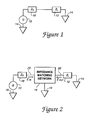
- an alternating current (ac) generator indicated by reference numeral 10 is connected to an electrical load 12.
- One terminal of the generator and one terminal of the load are connected to ground, as indicated at 14.
- Maximum power transfer from the generator 10 to the load 12 occurs when the output impedance Z G of the generator, indicated at 16, is the complex conjugate of the impedance Z L of the load 12.
- generator and load impedances do not match exactly, and an impedance matching network 18 is installed between the generator 10 and the load 12, as shown in Fig. 2.
- the generator impedance 16 is purely resistive for most practical purposes, and is indicated in Fig. 2 as having a value Z G .
- the input impedance of the network 18 with the load connected, as seen looking into the network on input line 20, is Z IN
- the output impedance of the network, with the generator connected, as seen looking back into the network on output line 22, is Z ouT .
- Z IN is the complex conjugate of Z G
- Z OUT is the complex conjugate of Z L .
- U.S. Patent 5 187 454 (Serial No. 07/825,658) discloses a control technique in which variable network values in the impedance matching network 18 are iteratively adjusted to converge on a solution based on values that are repeatedly predicted by a mathematical model of the network.
- the typical situation involving impedance matching is one in which the generator or source impedance is fixed and the load impedance is unknown and may vary.
- the task of impedance matching can be viewed as adjusting the network values until the input impedance Z IN matches the conjugate of the generator impedance Z G .
- the matching network is in a pi configuration, including a fixed series inductor 70 and two shunt circuits, one on each side of the fixed inductor.
- element 70 may be a fixed capacitance, rather than an inductance.
- the first shunt circuit, in parallel with the generator (not shown in Fig. 3) has a fixed capacitor 72 and a variable inductor 74 connected in parallel.
- the other shunt circuit in parallel with the load 12, has fixed capacitor 76 and a variable inductor 78 connected in parallel.
- Each of the variable inductors 74 and 78 has control inputs 79 for input of dc control currents, indicated as I and J.
- the load 12 might include, for example, a bias electrode in a plasma chamber. A return path will be provided through walls of the chamber, or through some other electrode, and the nature of the impedance will be predominantly capacitive, with a resistive power dissipating component.
- Each of the shunt circuits such as 72, 74 is electrically equivalent to a capacitor or an inductor; when the impedance matching network 18 is operated at a frequency above the resonant frequency 11VL, Cl, the shunt circuit behaves as a capacitor, below the resonant frequency, the shunt circuit behaves as an inductor.
- the variable inductor value is designed to provide an adjustment range of approximately 30-40 percent of the inductor's nominal value. For example, an inductor having a nominal inductance value of 10 /1.H (microhenries) might be made adjustable down to a value of approximately 6.5 /1.H.
- the X symbols in the diagram represent current transformers, by means of which current measurements are taken in each circuit branch in which an impedance is connected. Voltage is measured at the output of the network, as indicated at Y, and the network input voltage is already known from forward and reflected voltage measurements taken at the input. Specifically, the input voltage is the algebraic sum of the forward and reflected voltages. From these current and voltage measurements, the actual impedance values can be calculated for each of the impedances in the network. These calculated values are used to make corrections to the network model at each iteration of the control process.
- the circuit of Fig. 4 differs in that the load 12' is positioned in the series-connected position of the fixed inductance 70 of the Fig. 6 configuration.
- the network 18' includes fixed capacitors 72' and 76' and variable inductors 74' and 78', connected in much the same manner as in Fig. 6.
- the circuit 18' has its output nodes connected to lines 20 and 22, instead of between line 22 and ground. Accordingly, although the two configurations are outwardly similar, different network models are needed for the two configurations.
- the symbols X and Y indicate locations at which measurements of current and voltage, respectively, are taken.
- the shunt circuits comprise a variable inductance in parallel with a fixed capacitance. This is the preferred configuration because it allows one end of both the capacitor and inductor to be connected to ground.
- a series configuration could also be used to similar effect, although the behavior of the series combination would be the opposite of the parallel combination: the series combination would behave as a capacitor below the resonant frequency and an inductor above the resonant frequency.
- Fig. 5 is a diagrammatic depiction of one of the variable inductors used in the matching network of the presently preferred embodiment of the invention.
- the inductor consists of a cylindrical core 80 of soft ferrite material, or ferromagnetic or antiferromagnetic material, on which is wound an inductive coil 82, having terminals 84 for connection to the matching network 18 or 18'.
- the coil 82 is positioned near the center of the core 80.
- Near the ends of the core 80 are two control windings 86 and 88, through which dc control currents are applied through the terminals 79.
- the control windings 86 and 88 are shown as being connected in parallel, but may also be designed to be connected in series.
- variable inductance depicted in Fig. 5 has the advantage that it is easier to manufacture than coils of toroidal configuration. Moreover, the right-cylindrical design lends itself to liquid cooling by simply enclosing the core in a cooling jacket through which a liquid, such as deionized water, can be circulated. The windings may also be cooled, if necessary, by passing fluid through hollow conductors forming the windings, or by other means.
- An important aspect of the variable inductor design is that care must be taken to inhibit transformer action in which alternating current from the inductive coil 82 might be induced in the dc control windings 86 and 88. Transformer action can be minimized by a combination of electrostatic shielding of the control windings and appropriate filtering in the circuit supplying the control windings, and by physical separation of the control windings from the inductive coil.
- Core 80 is 7t inches high by % inch in diameter, and is suspended in a cavity filled with cooling water or other liquid.
- the cooling water cavity is defined by endpieces 90 (which have a top-hat shape, as illustrated in Fig. 6C) and a casting 92 (which has a cylindrical shape).
- the cooling water flows through the cavity in the direction indicated at 93.
- the core is suspended in the center of the cavity by plastic spiders 94 positioned between the ends of the core and the endpieces 90.
- Inductive coil 82 and control windings 86 and 88 are encased in alumina-filled epoxy castings.
- the control windings 86, 88 each contain approximately 100 turns and are formed into a toroidal shape having a 1 by 1 inch square cross-section. Taps 79 emerge from each end of each control winding and can be connecting to a suitable driving current source.
- the coil 82 contains 5-7 turns, and is approximately half as long as rod 80, or about 3% inches long.
- the diameter of the coil 82 is as close as possible to that of the core 80, e.g. about 1 inch, to minimize leakage flux which would reduce the range of adjustment of the permeability ( ⁇ ) of the core 80 and thus therefore the adjustment range of the inductance of the coil 82.
- One end of coil 82 contains a single tap 84 which is connected to ground; the other end of coil 82 contains three different taps - the inductance range of the coil 82 is chosen by attaching node 20 or 22 (Fig. 3, 4) to the appropriate one of these three taps.
- the core material is a ceramic ferrite rod manufactured by National Magnetics.
- the inductance of a 6 turn coil operating at 1.8-2 MHz, with zero control winding current is approximately 4 ⁇ H; at 30 Amps of control winding current, he inductance reduces to approximately 2 ⁇ H.
- Fig. 6A design provides for effective cooling.
- the control winding castings are formed so as to fit tightly to and in thermal contact with the endpieces 90.
- the alumina-filled epoxy casts, and the endpieces 90 are manufactured of materials with high heat conductivities and low heat capacities, so that the flow of cooling water cools not only the core but also the coil and control windings.
- FIG. 6A Another advantage of the Fig. 6A design is that it electro-magnetically decouples the control windings 86 and 88 from the coil 82. If endpieces 90 are made of a conductive material (e.g., metal), they will serve as Faraday shields which buck substantially all of the high-frequency magnetic fields emitted by coil 82, preventing these magnetic fields from coupling to the control windings 86 and 88 and creating high-frequency transformer effects between coil 82 and control windings 86 and 88.
- endpieces 90 are made of a conductive material (e.g., metal), they will serve as Faraday shields which buck substantially all of the high-frequency magnetic fields emitted by coil 82, preventing these magnetic fields from coupling to the control windings 86 and 88 and creating high-frequency transformer effects between coil 82 and control windings 86 and 88.
- low frequency magnetic fields such as those emitted by control windings 86 and 88 are substantially unaffected by the endpieces 90 (because the endpieces are not perfect conductors), and as a result these low frequency magnetic fields penetrate through the core 80 and thereby change the permeability of the core and the inductance of coil 82.
- Fig. 6A design Another advantage of the Fig. 6A design is low loss. Networks which use the Fig. 6A design have demonstrated efficiencies of approximately 95%. This efficiency is achieved by minimizing each of the potential sources of loss (e.g., eddy currents, hysteresis, and resistance losses), in the manner discussed below.
- loss e.g., eddy currents, hysteresis, and resistance losses
- core 80 is manufactured of a ceramic magnetic material which has low conductivity eddy current losses in the core are minimized.
- deionized water can be used and a non-conductive epoxy is used to encase the coil and control windings in castings.
- the endpieces contain a small gap 96 as shown in Fig. 6C, so that there is no continuous conductive path around the endpiece. (A negligible amount of high-frequency magnetic field penetrates gap 96.)
- High-frequency hysteresis losses in the core 80 are also reduced by this design.
- the primary design feature is the fact that core 80 is "gapped", that is, magnetic field (H) lines generated by the coil 82 must travel outside of the core 80.
- the core 80 is manufactured from a ferrite having a low loss tangent.
- the low frequency excitation level of the core is kept at a minimum by selecting values for Li, L 2 , L 3 , C 1 and C 2 which place the desired impedance near the center of the tunable range, thus reducing the control current amplitudes. (The relationship of the L and C values to the tunable range is discussed below with reference to Figs. 8A and 8B.)
- the excitation level can also be reduced by a local matching circuit (discussed below with reference to Fig. 9) which translates the impedance of the load into a region in which it can be more easily matched.
- Resistance losses are minimized by using large conductor wires and by cooling the windings and coil to a temperature near to the manufacturer's specifications, thereby preventing runaway.
- the electrical load is a plasma process.
- power is coupled to the process by two different means.
- Source power for the process is inductively coupled via an inductive antenna into a process chamber, and bias power for the same plasma process is applied through a bias electrode 102 in the chamber.
- Electrode 104 is grounded, and electrode 102 is driven by RF power from transmission line input 106 via high-capacitance coupling capacitor 108, which can be ignored for purposes of the RF design.
- a matching network is used for each of these loads. (Impedance matching of the bias load is not initiated until the principal, inductively coupled, load is impedance-matched to a desired degree.)
- Plasma initiation requires that a sufficient electric field magnitude be developed within the gas in the plasma chamber.
- US Patent 5 187 454 (Serial No. 07/825,658) describes control techniques for fine tuning the impedance matching circuits of Figs. 3 and 4 during plasma initiation and maintaining this tuning during the subsequent steady-state plasma process.
- variable inductances 74 and 78 are referred to as L 1 and L 2 , respectively.
- Fixed inductance 70 is referred to as L 3 .
- Capacitors 72 and 76 are referred to as C 1 and C 2 , respectively.
- the network is controlled by adjusting the variable inductance elements 74 and 78; the control variables are multipliers ⁇ 1 and a 2 , whose values lie between 0 and 1.
- the effective inductances of elements 74 and 78 are ⁇ 1 L 1 and ⁇ 2 L 2 , thus the multipliers ⁇ 1 and a 2 represent the effective inductances of elements 74 and 78 as a fraction of their maximum inductances L 1 and L 2 , respectively.
- the output impedance Z OUT seen by the load 12 is the complex conjugate of the load impedance Z L .
- the first step in selecting values for Li, C 1 , L 2 , C 2 and L 3 is to form an expression for the complex conjugate of the output impedance Z OUT of the circuit of Fig. 3 in terms of the values of the circuit element impedances and the impedance of the generator Z G 16 (Fig. 2).
- Fig. 8A illustrates the curves generated by varying a 2 while ⁇ 1 is maintained at constant values.
- Each of these curves of constant ⁇ 1 is a circle whose center lies on the real axis, and which contains the origin (0+j0). Not all of the circle is contained in the tuning range due to the limited range of a 2 .
- the diameter of each circle depends on the value chosen for ⁇ 1 and the values of the fixed components Ci, C 2 and L 3 .
- Fig. 8B illustrates the curves generated by varying ⁇ 1 while a 2 is maintained at a constant value.
- Each of the curves of constant a 2 is also a circle, but these are offset; each is tangent to the innermost of the circles of constant ⁇ 1 (110) and also tangent to the imaginary axis. The diameter of each of these circles depends on the value of a 2 and the values of the fixed components Ci, C 2 , and L 3 .
- Fig. 8C shows the curves of Figs. 8A and 8B superimposed to show the relationships described above.
- the designer chooses the operating frequency ⁇ .
- the inner limit circle (curve 110) is specified by its real intercept p i .
- No load impedance lying inside this circle can be matched to the target generator impedance by the network.
- L 3 is then provided by the following equation: where indicates the real-part operation.
- the desired values for L 1 and C 1 can then be determined by first computing the range for the parallel combination of L 1 and C 1 , denoted as Z 1 .
- Z 1 is defined as [(1/ ⁇ L 1 )- ⁇ C 1 ] -1 .
- the range of Z 1 is as follows: In ⁇ indicates the imaginary-part operation.
- the designer can then compute values for L 2 and C 2 by deciding upon the desired shape of the arcs of Fig. 8B.
- the locations of the centers of curvature of these arcs are related to the values of L 2 and C 2 ; therefore, by choosing the desired center of curvature for two of the arcs, the designer can determine the desired values for L 2 and C 2 .
- the limiting curves 114 and 116 can be specified by the real parts of their centers.
- the real component of the center of arc 114 be referred to as ⁇ 3 and the real component of the center of arc 116 will be referred to as p 4 .
- p 3 and p 4 are related to L 2 and C 2 by the following equations: where Z 2 is defined as [(1/ ⁇ L2)- ⁇ C 2 ] -1 .
- C 2 and L 2 can be found by computing the range limits for Z 2 from these equations and then solving simultaneous equations (analogous to equations (5)) relating Z 2 to L 2 , C 2 , and ⁇ 2,MIN.
- the graphs of Figs. 8A and 8B were generated for the circuit of Fig. 3 as configured to allow matching with the source antenna 100 of the plasma process illustrated in Fig. 7.
- the circuit of Fig. 3 may be configured to allow matching the driving impedance of the bias electrode 102 of Fig. 7.
- a plasma loaded inductive antenna has a complex impedance with a relatively large positive imaginary part and a relatively small real part. If such an impedance were plotted in Figs. 8A, 8B, or 8C, it would lie well above the upper left corner of the graphs.
- a network such as that shown in Fig. 9.
- a designer can compute values for C 1 and C 2 which will achieve a desired impedance Z e at input line 22 by measuring of the impedance, Zp, of the source antenna coil 100 and the plasma loading it, and then applying the following formulas:
- the impedance of a plasma contained in a chamber such as illustrated in Fig. 7, not including the source antenna coil 100 has been empirically measured at 12-j10.
- the plasma and antenna impedance which will be referred to as Zp, is equal to 12+j( ⁇ L a -10).
- the present invention represents a significant advance in the field of dynamic impedance matching networks, to maximize the power transferred to the load.
- the invention provides a reliable technique for matching a source impedance with a variable and unknown load impedance. It will also be appreciated that, although a specific embodiment of the invention has been described in detail by way of illustration, various modifications may be made without departing from the spirit and scope of the invention. Accordingly, the invention is not to be limited except as by the appended claims.
Landscapes
- Engineering & Computer Science (AREA)
- Physics & Mathematics (AREA)
- Plasma & Fusion (AREA)
- Chemical & Material Sciences (AREA)
- Analytical Chemistry (AREA)
- Power Engineering (AREA)
- Electromagnetism (AREA)
- Spectroscopy & Molecular Physics (AREA)
- Health & Medical Sciences (AREA)
- Epidemiology (AREA)
- Public Health (AREA)
- Plasma Technology (AREA)
Priority Applications (1)
| Application Number | Priority Date | Filing Date | Title |
|---|---|---|---|
| EP97118731A EP0825712A3 (fr) | 1992-11-12 | 1993-11-12 | Circuit d'adaptation d'accord électronique utilisant des éléments d'inductance ajustables et circuits oscillants |
Applications Claiming Priority (2)
| Application Number | Priority Date | Filing Date | Title |
|---|---|---|---|
| US07/975,355 US5392018A (en) | 1991-06-27 | 1992-11-12 | Electronically tuned matching networks using adjustable inductance elements and resonant tank circuits |
| US975355 | 1992-11-12 |
Related Child Applications (1)
| Application Number | Title | Priority Date | Filing Date |
|---|---|---|---|
| EP97118731A Division EP0825712A3 (fr) | 1992-11-12 | 1993-11-12 | Circuit d'adaptation d'accord électronique utilisant des éléments d'inductance ajustables et circuits oscillants |
Publications (1)
| Publication Number | Publication Date |
|---|---|
| EP0597497A1 true EP0597497A1 (fr) | 1994-05-18 |
Family
ID=25522940
Family Applications (2)
| Application Number | Title | Priority Date | Filing Date |
|---|---|---|---|
| EP93118387A Withdrawn EP0597497A1 (fr) | 1992-11-12 | 1993-11-12 | Circuit d'adaptation d'accord électronique utilisant des éléments d'inductance ajustables et circuits oscillants |
| EP97118731A Withdrawn EP0825712A3 (fr) | 1992-11-12 | 1993-11-12 | Circuit d'adaptation d'accord électronique utilisant des éléments d'inductance ajustables et circuits oscillants |
Family Applications After (1)
| Application Number | Title | Priority Date | Filing Date |
|---|---|---|---|
| EP97118731A Withdrawn EP0825712A3 (fr) | 1992-11-12 | 1993-11-12 | Circuit d'adaptation d'accord électronique utilisant des éléments d'inductance ajustables et circuits oscillants |
Country Status (4)
| Country | Link |
|---|---|
| US (3) | US5392018A (fr) |
| EP (2) | EP0597497A1 (fr) |
| JP (1) | JPH06215955A (fr) |
| KR (1) | KR940012819A (fr) |
Cited By (16)
| Publication number | Priority date | Publication date | Assignee | Title |
|---|---|---|---|---|
| EP0714106A1 (fr) * | 1994-10-27 | 1996-05-29 | Applied Materials, Inc. | Inductance variable, circuit d'adaptation et système de traitement par plasma comportant une telle inductance |
| WO2001063982A1 (fr) * | 2000-02-24 | 2001-08-30 | C C R Gmbh Beschichtungstechnologie | Reseau a quatre fils haute frequence |
| WO2001063981A1 (fr) * | 2000-02-24 | 2001-08-30 | Ccr Gmbh Beschichtungstechno Logie | Source de plasma haute frequence |
| US7700164B2 (en) | 1993-07-20 | 2010-04-20 | Semiconductor Energy Laboratory Co., Ltd | Apparatus for fabricating coating and method of fabricating the coating |
| CN109526082A (zh) * | 2017-11-17 | 2019-03-26 | 恩智浦美国有限公司 | 用于阻抗网络调谐的具有相位检测的射频加热系统 |
| WO2019096564A1 (fr) * | 2017-11-17 | 2019-05-23 | Evatec Ag | Fourniture d'énergie radiofréquence (rf) à un traitement au plasma sous vide |
| US10616963B2 (en) | 2016-08-05 | 2020-04-07 | Nxp Usa, Inc. | Apparatus and methods for detecting defrosting operation completion |
| US10785834B2 (en) | 2017-12-15 | 2020-09-22 | Nxp Usa, Inc. | Radio frequency heating and defrosting apparatus with in-cavity shunt capacitor |
| US10917948B2 (en) | 2017-11-07 | 2021-02-09 | Nxp Usa, Inc. | Apparatus and methods for defrosting operations in an RF heating system |
| US10952289B2 (en) | 2018-09-10 | 2021-03-16 | Nxp Usa, Inc. | Defrosting apparatus with mass estimation and methods of operation thereof |
| US11039512B2 (en) | 2016-08-05 | 2021-06-15 | Nxp Usa, Inc. | Defrosting apparatus with lumped inductive matching network and methods of operation thereof |
| US11039511B2 (en) | 2018-12-21 | 2021-06-15 | Nxp Usa, Inc. | Defrosting apparatus with two-factor mass estimation and methods of operation thereof |
| US11166352B2 (en) | 2018-12-19 | 2021-11-02 | Nxp Usa, Inc. | Method for performing a defrosting operation using a defrosting apparatus |
| US11382190B2 (en) | 2017-12-20 | 2022-07-05 | Nxp Usa, Inc. | Defrosting apparatus and methods of operation thereof |
| US11570857B2 (en) | 2018-03-29 | 2023-01-31 | Nxp Usa, Inc. | Thermal increase system and methods of operation thereof |
| US11800608B2 (en) | 2018-09-14 | 2023-10-24 | Nxp Usa, Inc. | Defrosting apparatus with arc detection and methods of operation thereof |
Families Citing this family (92)
| Publication number | Priority date | Publication date | Assignee | Title |
|---|---|---|---|---|
| US6077384A (en) | 1994-08-11 | 2000-06-20 | Applied Materials, Inc. | Plasma reactor having an inductive antenna coupling power through a parallel plate electrode |
| US6165311A (en) * | 1991-06-27 | 2000-12-26 | Applied Materials, Inc. | Inductively coupled RF plasma reactor having an overhead solenoidal antenna |
| US6514376B1 (en) | 1991-06-27 | 2003-02-04 | Applied Materials Inc. | Thermal control apparatus for inductively coupled RF plasma reactor having an overhead solenoidal antenna |
| US6488807B1 (en) | 1991-06-27 | 2002-12-03 | Applied Materials, Inc. | Magnetic confinement in a plasma reactor having an RF bias electrode |
| US6074512A (en) * | 1991-06-27 | 2000-06-13 | Applied Materials, Inc. | Inductively coupled RF plasma reactor having an overhead solenoidal antenna and modular confinement magnet liners |
| US6063233A (en) | 1991-06-27 | 2000-05-16 | Applied Materials, Inc. | Thermal control apparatus for inductively coupled RF plasma reactor having an overhead solenoidal antenna |
| US6238588B1 (en) | 1991-06-27 | 2001-05-29 | Applied Materials, Inc. | High pressure high non-reactive diluent gas content high plasma ion density plasma oxide etch process |
| US6036877A (en) | 1991-06-27 | 2000-03-14 | Applied Materials, Inc. | Plasma reactor with heated source of a polymer-hardening precursor material |
| US5477975A (en) * | 1993-10-15 | 1995-12-26 | Applied Materials Inc | Plasma etch apparatus with heated scavenging surfaces |
| US6090303A (en) * | 1991-06-27 | 2000-07-18 | Applied Materials, Inc. | Process for etching oxides in an electromagnetically coupled planar plasma apparatus |
| US6024826A (en) * | 1996-05-13 | 2000-02-15 | Applied Materials, Inc. | Plasma reactor with heated source of a polymer-hardening precursor material |
| US5907221A (en) * | 1995-08-16 | 1999-05-25 | Applied Materials, Inc. | Inductively coupled plasma reactor with an inductive coil antenna having independent loops |
| TW279240B (en) | 1995-08-30 | 1996-06-21 | Applied Materials Inc | Parallel-plate icp source/rf bias electrode head |
| JPH09180897A (ja) * | 1995-12-12 | 1997-07-11 | Applied Materials Inc | 高密度プラズマリアクタのためのガス供給装置 |
| US6054013A (en) | 1996-02-02 | 2000-04-25 | Applied Materials, Inc. | Parallel plate electrode plasma reactor having an inductive antenna and adjustable radial distribution of plasma ion density |
| US6036878A (en) | 1996-02-02 | 2000-03-14 | Applied Materials, Inc. | Low density high frequency process for a parallel-plate electrode plasma reactor having an inductive antenna |
| US6440221B2 (en) | 1996-05-13 | 2002-08-27 | Applied Materials, Inc. | Process chamber having improved temperature control |
| US5770982A (en) * | 1996-10-29 | 1998-06-23 | Sematech, Inc. | Self isolating high frequency saturable reactor |
| GB9708268D0 (en) | 1997-04-24 | 1997-06-18 | Gyrus Medical Ltd | An electrosurgical instrument |
| US6579426B1 (en) | 1997-05-16 | 2003-06-17 | Applied Materials, Inc. | Use of variable impedance to control coil sputter distribution |
| US6652717B1 (en) * | 1997-05-16 | 2003-11-25 | Applied Materials, Inc. | Use of variable impedance to control coil sputter distribution |
| US6178920B1 (en) | 1997-06-05 | 2001-01-30 | Applied Materials, Inc. | Plasma reactor with internal inductive antenna capable of generating helicon wave |
| US6345588B1 (en) | 1997-08-07 | 2002-02-12 | Applied Materials, Inc. | Use of variable RF generator to control coil voltage distribution |
| US6235169B1 (en) | 1997-08-07 | 2001-05-22 | Applied Materials, Inc. | Modulated power for ionized metal plasma deposition |
| US6375810B2 (en) | 1997-08-07 | 2002-04-23 | Applied Materials, Inc. | Plasma vapor deposition with coil sputtering |
| US6023038A (en) * | 1997-09-16 | 2000-02-08 | Applied Materials, Inc. | Resistive heating of powered coil to reduce transient heating/start up effects multiple loadlock system |
| US6132551A (en) * | 1997-09-20 | 2000-10-17 | Applied Materials, Inc. | Inductive RF plasma reactor with overhead coil and conductive laminated RF window beneath the overhead coil |
| US6281794B1 (en) * | 1998-01-02 | 2001-08-28 | Intermec Ip Corp. | Radio frequency transponder with improved read distance |
| US6254738B1 (en) | 1998-03-31 | 2001-07-03 | Applied Materials, Inc. | Use of variable impedance having rotating core to control coil sputter distribution |
| US6155199A (en) * | 1998-03-31 | 2000-12-05 | Lam Research Corporation | Parallel-antenna transformer-coupled plasma generation system |
| US6164241A (en) | 1998-06-30 | 2000-12-26 | Lam Research Corporation | Multiple coil antenna for inductively-coupled plasma generation systems |
| TW434636B (en) | 1998-07-13 | 2001-05-16 | Applied Komatsu Technology Inc | RF matching network with distributed outputs |
| US6211498B1 (en) * | 1999-03-01 | 2001-04-03 | Powell Power Electronics, Inc. | Induction heating apparatus and transformer |
| US6589437B1 (en) | 1999-03-05 | 2003-07-08 | Applied Materials, Inc. | Active species control with time-modulated plasma |
| US6401652B1 (en) | 2000-05-04 | 2002-06-11 | Applied Materials, Inc. | Plasma reactor inductive coil antenna with flat surface facing the plasma |
| AU2002227418A1 (en) * | 2001-01-22 | 2002-08-06 | Tokyo Electron Limited | Vertically translatable chuck assembly and method for a plasma reactor system |
| KR100444189B1 (ko) * | 2001-03-19 | 2004-08-18 | 주성엔지니어링(주) | 유도결합 플라즈마 소스의 임피던스 정합 회로 |
| US7394430B2 (en) | 2001-04-11 | 2008-07-01 | Kyocera Wireless Corp. | Wireless device reconfigurable radiation desensitivity bracket systems and methods |
| US7174147B2 (en) * | 2001-04-11 | 2007-02-06 | Kyocera Wireless Corp. | Bandpass filter with tunable resonator |
| US7221243B2 (en) | 2001-04-11 | 2007-05-22 | Kyocera Wireless Corp. | Apparatus and method for combining electrical signals |
| US6690251B2 (en) | 2001-04-11 | 2004-02-10 | Kyocera Wireless Corporation | Tunable ferro-electric filter |
| US7154440B2 (en) | 2001-04-11 | 2006-12-26 | Kyocera Wireless Corp. | Phase array antenna using a constant-gain phase shifter |
| US7164329B2 (en) | 2001-04-11 | 2007-01-16 | Kyocera Wireless Corp. | Tunable phase shifer with a control signal generator responsive to DC offset in a mixed signal |
| US7746292B2 (en) | 2001-04-11 | 2010-06-29 | Kyocera Wireless Corp. | Reconfigurable radiation desensitivity bracket systems and methods |
| GB2380871B (en) * | 2001-07-30 | 2003-09-24 | Tunewell Technology Ltd | Improvements in or relating to a power distribution system |
| US7071776B2 (en) | 2001-10-22 | 2006-07-04 | Kyocera Wireless Corp. | Systems and methods for controlling output power in a communication device |
| US7037298B2 (en) * | 2001-12-20 | 2006-05-02 | The Procter & Gamble Company | Disposable absorbent article having a raised circumferential bank |
| JP4024053B2 (ja) | 2002-02-08 | 2007-12-19 | キヤノンアネルバ株式会社 | 高周波プラズマ処理方法及び高周波プラズマ処理装置 |
| US7180467B2 (en) * | 2002-02-12 | 2007-02-20 | Kyocera Wireless Corp. | System and method for dual-band antenna matching |
| US7176845B2 (en) | 2002-02-12 | 2007-02-13 | Kyocera Wireless Corp. | System and method for impedance matching an antenna to sub-bands in a communication band |
| US7184727B2 (en) | 2002-02-12 | 2007-02-27 | Kyocera Wireless Corp. | Full-duplex antenna system and method |
| JP4439169B2 (ja) * | 2002-09-10 | 2010-03-24 | 株式会社アルバック | 真空処理方法及び真空装置 |
| US20040149219A1 (en) * | 2002-10-02 | 2004-08-05 | Tomohiro Okumura | Plasma doping method and plasma doping apparatus |
| US7212078B2 (en) * | 2003-02-25 | 2007-05-01 | Tokyo Electron Limited | Method and assembly for providing impedance matching network and network assembly |
| US7264419B2 (en) * | 2003-03-19 | 2007-09-04 | Applied Process Technology, Inc. | System and method for remediating contaminated soil and groundwater in situ |
| US7720443B2 (en) | 2003-06-02 | 2010-05-18 | Kyocera Wireless Corp. | System and method for filtering time division multiple access telephone communications |
| US7042311B1 (en) * | 2003-10-10 | 2006-05-09 | Novellus Systems, Inc. | RF delivery configuration in a plasma processing system |
| JP4192775B2 (ja) * | 2003-12-05 | 2008-12-10 | 株式会社ダイフク | 無接触給電設備 |
| US7326872B2 (en) * | 2004-04-28 | 2008-02-05 | Applied Materials, Inc. | Multi-frequency dynamic dummy load and method for testing plasma reactor multi-frequency impedance match networks |
| US7248845B2 (en) | 2004-07-09 | 2007-07-24 | Kyocera Wireless Corp. | Variable-loss transmitter and method of operation |
| US20060105114A1 (en) * | 2004-11-16 | 2006-05-18 | White John M | Multi-layer high quality gate dielectric for low-temperature poly-silicon TFTs |
| US8187416B2 (en) * | 2005-05-20 | 2012-05-29 | Applied Materials, Inc. | Interior antenna for substrate processing chamber |
| US7518466B2 (en) * | 2005-08-29 | 2009-04-14 | Applied Materials, Inc. | Methods and apparatus for symmetrical and/or concentric radio frequency matching networks |
| US20070080141A1 (en) * | 2005-10-07 | 2007-04-12 | Applied Materials, Inc. | Low-voltage inductively coupled source for plasma processing |
| US7548762B2 (en) | 2005-11-30 | 2009-06-16 | Kyocera Corporation | Method for tuning a GPS antenna matching network |
| US20080118663A1 (en) * | 2006-10-12 | 2008-05-22 | Applied Materials, Inc. | Contamination reducing liner for inductively coupled chamber |
| CN101188159B (zh) * | 2006-11-24 | 2011-01-12 | 阎跃军 | 分段可调电感器 |
| JP5606312B2 (ja) * | 2007-07-23 | 2014-10-15 | トゥルンプフ ヒュッティンガー ゲゼルシャフト ミット ベシュレンクテル ハフツング ウント コンパニー コマンディートゲゼルシャフト | プラズマ給電装置 |
| EP2145978A1 (fr) * | 2008-07-16 | 2010-01-20 | AGC Flat Glass Europe SA | Procédé et installation pour le dépôt de couches sur un substrat |
| US8922315B2 (en) | 2011-05-17 | 2014-12-30 | Bae Systems Information And Electronic Systems Integration Inc. | Flexible ultracapacitor cloth for feeding portable electronic device |
| ITPV20110015A1 (it) * | 2011-08-05 | 2013-02-06 | Bdiscom Srl | Adattore di impedenza semifisso facente uso di induttori variabili per processi in plasma a bassa pressione |
| US8776002B2 (en) * | 2011-09-06 | 2014-07-08 | Variable Z0, Ltd. | Variable Z0 antenna device design system and method |
| US10157729B2 (en) | 2012-02-22 | 2018-12-18 | Lam Research Corporation | Soft pulsing |
| US20130319450A1 (en) * | 2012-06-03 | 2013-12-05 | M.M. & R. Products, Inc. | Hairstyling Tool With Automatically Reversing Cylinder |
| TWI508367B (zh) * | 2012-09-27 | 2015-11-11 | Ind Tech Res Inst | 通訊裝置及其天線元件之設計方法 |
| US9082589B2 (en) * | 2012-10-09 | 2015-07-14 | Novellus Systems, Inc. | Hybrid impedance matching for inductively coupled plasma system |
| US9460894B2 (en) | 2013-06-28 | 2016-10-04 | Lam Research Corporation | Controlling ion energy within a plasma chamber |
| US10512553B2 (en) * | 2014-07-30 | 2019-12-24 | The Alfred E. Mann Foundation For Scientific Research | Inductive link coil de-tuning compensation and control |
| KR102432150B1 (ko) | 2014-08-15 | 2022-08-11 | 어플라이드 머티어리얼스, 인코포레이티드 | 플라즈마 프로세싱 시스템들을 위한 소형의 구성 가능한 모듈형 무선 주파수 매칭 네트워크 조립체 |
| US10923322B2 (en) | 2017-06-14 | 2021-02-16 | Lam Research Corporation | Articulated direct-mount inductor and associated systems and methods |
| KR102791775B1 (ko) | 2019-05-07 | 2025-04-03 | 램 리써치 코포레이션 | 폐루프 다중 출력 rf 매칭 |
| US11107661B2 (en) * | 2019-07-09 | 2021-08-31 | COMET Technologies USA, Inc. | Hybrid matching network topology |
| CN118866641A (zh) | 2019-07-31 | 2024-10-29 | 朗姆研究公司 | 具有多个输出端口的射频功率产生器 |
| WO2021113387A1 (fr) | 2019-12-02 | 2021-06-10 | Lam Research Corporation | Transformation d'impédance dans la génération de plasma assistée par radiofréquence |
| US11994542B2 (en) | 2020-03-27 | 2024-05-28 | Lam Research Corporation | RF signal parameter measurement in an integrated circuit fabrication chamber |
| KR20230021739A (ko) | 2020-06-12 | 2023-02-14 | 램 리써치 코포레이션 | Rf 커플링 구조체들에 의한 플라즈마 형성의 제어 |
| US11348761B2 (en) * | 2020-09-04 | 2022-05-31 | Tokyo Electron Limited | Impedance matching apparatus and control method |
| KR102787323B1 (ko) | 2020-09-24 | 2025-03-27 | 삼성전자주식회사 | 플라즈마 처리 장치 및 플라즈마 처리 방법 |
| US12198908B2 (en) * | 2021-05-11 | 2025-01-14 | Applied Materials, Inc. | Magnetically coupled RF filter for substrate processing chambers |
| US12020902B2 (en) | 2022-07-14 | 2024-06-25 | Tokyo Electron Limited | Plasma processing with broadband RF waveforms |
| JP2024046847A (ja) * | 2022-09-26 | 2024-04-05 | 株式会社ダイヘン | 高電圧電気部品 |
| US20240347317A1 (en) * | 2023-04-11 | 2024-10-17 | Tokyo Electron Limited | Method and System for Plasma Processing |
Citations (2)
| Publication number | Priority date | Publication date | Assignee | Title |
|---|---|---|---|---|
| US4630013A (en) * | 1984-01-30 | 1986-12-16 | Toko Kabushiki Kaisha | Current controlled variable inductor |
| US5187454A (en) * | 1992-01-23 | 1993-02-16 | Applied Materials, Inc. | Electronically tuned matching network using predictor-corrector control system |
Family Cites Families (26)
| Publication number | Priority date | Publication date | Assignee | Title |
|---|---|---|---|---|
| US1708950A (en) * | 1925-05-12 | 1929-04-16 | Western Electric Co | Electric wave filter |
| US2052703A (en) * | 1933-03-07 | 1936-09-01 | Rca Corp | Coupled circuits |
| US2250519A (en) * | 1934-02-23 | 1941-07-29 | Rca Corp | Automatic tuning system |
| US2238260A (en) * | 1937-10-19 | 1941-04-15 | Lorenz C Ag | Electric filter arrangement |
| US2611030A (en) * | 1947-10-24 | 1952-09-16 | Carl G Sontheimer | Energy transfer system |
| GB670680A (en) * | 1949-10-13 | 1952-04-23 | Gen Electric Co Ltd | Improvements in or relating to electrical apparatus comprising saturable chokes |
| US2884632A (en) * | 1952-08-06 | 1959-04-28 | Cgs Lab Inc | Antenna tuning system |
| US2920323A (en) * | 1953-09-16 | 1960-01-05 | Philip M Dunson | Broad-band impedance matching |
| US2790954A (en) * | 1954-02-01 | 1957-04-30 | Rca Corp | Transient correcting network |
| US2807788A (en) * | 1954-07-02 | 1957-09-24 | Rca Corp | Radio frequency choke coils |
| USRE25712E (en) * | 1957-07-02 | 1965-01-19 | Super conductive switching element | |
| US3132313A (en) * | 1959-08-13 | 1964-05-05 | Alford Andrew | Impedance matching filter |
| US3019335A (en) * | 1959-09-14 | 1962-01-30 | Nat Company Inc | Large bandwidth low noise antenna circuit |
| FR2485192A1 (fr) * | 1980-06-19 | 1981-12-24 | Telecommunications Sa | Procede et dispositif pour mesurer la pression de pneumatiques notamment pour aeronefs |
| US4375051A (en) * | 1981-02-19 | 1983-02-22 | The Perkin-Elmer Corporation | Automatic impedance matching between source and load |
| US4433315A (en) * | 1981-11-24 | 1984-02-21 | General Electric Company | Tunable coupling network |
| US4518941A (en) * | 1983-11-16 | 1985-05-21 | Nihon Kohden Corporation | Pulse transformer for switching power supplies |
| US4621242A (en) * | 1984-03-19 | 1986-11-04 | The Perkin-Elmer Corporation | R.F. impedance match control system |
| US4586007A (en) * | 1984-10-22 | 1986-04-29 | Rca Corporation | Notch filter |
| JPH0777324B2 (ja) * | 1988-03-23 | 1995-08-16 | セイコーエプソン株式会社 | 腕装着型無線機 |
| US4977301A (en) * | 1988-10-13 | 1990-12-11 | Matsushita Electric Industrial Co., Ltd. | High-frequency heating apparatus using frequency-converter-type power supply |
| US4904972A (en) * | 1989-06-28 | 1990-02-27 | Hitachi, Ltd. | Gas-insulated stationary induction electrical apparatus |
| US4951009A (en) * | 1989-08-11 | 1990-08-21 | Applied Materials, Inc. | Tuning method and control system for automatic matching network |
| US5065118A (en) * | 1990-07-26 | 1991-11-12 | Applied Materials, Inc. | Electronically tuned VHF/UHF matching network |
| JP2519364B2 (ja) * | 1990-12-03 | 1996-07-31 | アプライド マテリアルズ インコーポレイテッド | Uhf/vhf共振アンテナ供給源を用いたプラズマリアクタ |
| US5202656A (en) * | 1991-10-22 | 1993-04-13 | Eagle Comtronics, Inc. | Frequency shifting tuning process and filter structure |
-
1992
- 1992-11-12 US US07/975,355 patent/US5392018A/en not_active Expired - Lifetime
-
1993
- 1993-11-11 JP JP5282663A patent/JPH06215955A/ja active Pending
- 1993-11-12 KR KR1019930023997A patent/KR940012819A/ko not_active Withdrawn
- 1993-11-12 EP EP93118387A patent/EP0597497A1/fr not_active Withdrawn
- 1993-11-12 EP EP97118731A patent/EP0825712A3/fr not_active Withdrawn
-
1994
- 1994-11-09 US US08/336,873 patent/US5574410A/en not_active Expired - Lifetime
-
1995
- 1995-08-22 US US08/518,014 patent/US5572170A/en not_active Expired - Lifetime
Patent Citations (3)
| Publication number | Priority date | Publication date | Assignee | Title |
|---|---|---|---|---|
| US4630013A (en) * | 1984-01-30 | 1986-12-16 | Toko Kabushiki Kaisha | Current controlled variable inductor |
| US5187454A (en) * | 1992-01-23 | 1993-02-16 | Applied Materials, Inc. | Electronically tuned matching network using predictor-corrector control system |
| EP0552955A1 (fr) * | 1992-01-23 | 1993-07-28 | Applied Materials, Inc. | Circuit d'adaptation d'accord électronique comportant un système de commande predicteur-correcteur |
Cited By (25)
| Publication number | Priority date | Publication date | Assignee | Title |
|---|---|---|---|---|
| US7700164B2 (en) | 1993-07-20 | 2010-04-20 | Semiconductor Energy Laboratory Co., Ltd | Apparatus for fabricating coating and method of fabricating the coating |
| US5585766A (en) * | 1994-10-27 | 1996-12-17 | Applied Materials, Inc. | Electrically tuned matching networks using adjustable inductance elements |
| EP0714106A1 (fr) * | 1994-10-27 | 1996-05-29 | Applied Materials, Inc. | Inductance variable, circuit d'adaptation et système de traitement par plasma comportant une telle inductance |
| WO2001063982A1 (fr) * | 2000-02-24 | 2001-08-30 | C C R Gmbh Beschichtungstechnologie | Reseau a quatre fils haute frequence |
| WO2001063981A1 (fr) * | 2000-02-24 | 2001-08-30 | Ccr Gmbh Beschichtungstechno Logie | Source de plasma haute frequence |
| US6936144B2 (en) | 2000-02-24 | 2005-08-30 | Ccr Gmbh Beschichtungstechnologie | High frequency plasma source |
| KR100740892B1 (ko) * | 2000-02-24 | 2007-07-19 | 체체에르 게엠베하 베쉬히퉁스테크놀로지 | 고주파 정합 회로망 |
| US10616963B2 (en) | 2016-08-05 | 2020-04-07 | Nxp Usa, Inc. | Apparatus and methods for detecting defrosting operation completion |
| US11039512B2 (en) | 2016-08-05 | 2021-06-15 | Nxp Usa, Inc. | Defrosting apparatus with lumped inductive matching network and methods of operation thereof |
| US10917948B2 (en) | 2017-11-07 | 2021-02-09 | Nxp Usa, Inc. | Apparatus and methods for defrosting operations in an RF heating system |
| US10771036B2 (en) | 2017-11-17 | 2020-09-08 | Nxp Usa, Inc. | RF heating system with phase detection for impedance network tuning |
| CN109526082A (zh) * | 2017-11-17 | 2019-03-26 | 恩智浦美国有限公司 | 用于阻抗网络调谐的具有相位检测的射频加热系统 |
| WO2019096564A1 (fr) * | 2017-11-17 | 2019-05-23 | Evatec Ag | Fourniture d'énergie radiofréquence (rf) à un traitement au plasma sous vide |
| CN111316396B (zh) * | 2017-11-17 | 2023-02-17 | 瑞士艾发科技 | 对真空等离子体处理的rf功率递送 |
| EP3487263A1 (fr) * | 2017-11-17 | 2019-05-22 | NXP USA, Inc. | Système de chauffage rf à détection de phase pour réglage de réseau d'impédance |
| US11380520B2 (en) | 2017-11-17 | 2022-07-05 | Evatec Ag | RF power delivery to vacuum plasma processing |
| CN109526082B (zh) * | 2017-11-17 | 2021-06-04 | 恩智浦美国有限公司 | 用于阻抗网络调谐的具有相位检测的射频加热系统 |
| CN111316396A (zh) * | 2017-11-17 | 2020-06-19 | 瑞士艾发科技 | 对真空等离子体处理的rf功率递送 |
| US10785834B2 (en) | 2017-12-15 | 2020-09-22 | Nxp Usa, Inc. | Radio frequency heating and defrosting apparatus with in-cavity shunt capacitor |
| US11382190B2 (en) | 2017-12-20 | 2022-07-05 | Nxp Usa, Inc. | Defrosting apparatus and methods of operation thereof |
| US11570857B2 (en) | 2018-03-29 | 2023-01-31 | Nxp Usa, Inc. | Thermal increase system and methods of operation thereof |
| US10952289B2 (en) | 2018-09-10 | 2021-03-16 | Nxp Usa, Inc. | Defrosting apparatus with mass estimation and methods of operation thereof |
| US11800608B2 (en) | 2018-09-14 | 2023-10-24 | Nxp Usa, Inc. | Defrosting apparatus with arc detection and methods of operation thereof |
| US11166352B2 (en) | 2018-12-19 | 2021-11-02 | Nxp Usa, Inc. | Method for performing a defrosting operation using a defrosting apparatus |
| US11039511B2 (en) | 2018-12-21 | 2021-06-15 | Nxp Usa, Inc. | Defrosting apparatus with two-factor mass estimation and methods of operation thereof |
Also Published As
| Publication number | Publication date |
|---|---|
| KR940012819A (ko) | 1994-06-24 |
| US5392018A (en) | 1995-02-21 |
| EP0825712A3 (fr) | 1998-03-11 |
| JPH06215955A (ja) | 1994-08-05 |
| US5574410A (en) | 1996-11-12 |
| US5572170A (en) | 1996-11-05 |
| EP0825712A2 (fr) | 1998-02-25 |
Similar Documents
| Publication | Publication Date | Title |
|---|---|---|
| EP0597497A1 (fr) | Circuit d'adaptation d'accord électronique utilisant des éléments d'inductance ajustables et circuits oscillants | |
| US5585766A (en) | Electrically tuned matching networks using adjustable inductance elements | |
| US5770982A (en) | Self isolating high frequency saturable reactor | |
| KR100932019B1 (ko) | 플라즈마 생성 장치 및 방법, 및 고주파 구동 회로 | |
| US5541482A (en) | Electrodeless discharge lamp including impedance matching and filter network | |
| JP4646272B2 (ja) | プラズマ加工装置 | |
| CN100569354C (zh) | 使等离子体源消除对于匹配电路的需要的方法 | |
| EP0412568A2 (fr) | Circuit d'adaptation et méthode pour son utilisation | |
| JP2007524963A (ja) | プラズマ生成装置及び方法並びに可変デューティサイクルの高周波駆動回路 | |
| US5065118A (en) | Electronically tuned VHF/UHF matching network | |
| KR20010096474A (ko) | 플라즈마 에칭 장치 | |
| US6211749B1 (en) | Impedance matching device | |
| US6288378B1 (en) | Induction heating system with split resonance capacitance | |
| CN112600314A (zh) | 用于传输电能的方法和装置 | |
| KR102610976B1 (ko) | 고전력 rf 나선 코일 필터 | |
| US5586017A (en) | Power generator comprising a transformer | |
| CN108075473B (zh) | 一种滤波电路、加热电路和半导体处理设备 | |
| KR101918357B1 (ko) | Radio-Frequency 전력 유도결합 플라즈마 발생장치 | |
| EP0641510B1 (fr) | Lampe a decharge sans electrodes comportant un reseau d'adaptation d'impedance et de filtrage | |
| JP2530560B2 (ja) | 高周波プラズマ用インピ―ダンス整合装置 | |
| CN109148073B (zh) | 线圈组件、等离子体发生装置及等离子体设备 | |
| US20190156985A1 (en) | High accuracy tuning of resonant network | |
| JPH0878994A (ja) | インピ−ダンス整合回路 | |
| Rajan | Design and Development of Wireless Power Transmission | |
| JPS6161503B2 (fr) |
Legal Events
| Date | Code | Title | Description |
|---|---|---|---|
| PUAI | Public reference made under article 153(3) epc to a published international application that has entered the european phase |
Free format text: ORIGINAL CODE: 0009012 |
|
| AK | Designated contracting states |
Kind code of ref document: A1 Designated state(s): DE ES FR GB IT NL |
|
| 17P | Request for examination filed |
Effective date: 19941018 |
|
| 17Q | First examination report despatched |
Effective date: 19960912 |
|
| GRAG | Despatch of communication of intention to grant |
Free format text: ORIGINAL CODE: EPIDOS AGRA |
|
| GRAG | Despatch of communication of intention to grant |
Free format text: ORIGINAL CODE: EPIDOS AGRA |
|
| GRAH | Despatch of communication of intention to grant a patent |
Free format text: ORIGINAL CODE: EPIDOS IGRA |
|
| STAA | Information on the status of an ep patent application or granted ep patent |
Free format text: STATUS: THE APPLICATION IS DEEMED TO BE WITHDRAWN |
|
| 18D | Application deemed to be withdrawn |
Effective date: 19981111 |