EP0597603A2 - Planarisation d'une ramure d'isolation utilisant un masque dur - Google Patents
Planarisation d'une ramure d'isolation utilisant un masque dur Download PDFInfo
- Publication number
- EP0597603A2 EP0597603A2 EP93308495A EP93308495A EP0597603A2 EP 0597603 A2 EP0597603 A2 EP 0597603A2 EP 93308495 A EP93308495 A EP 93308495A EP 93308495 A EP93308495 A EP 93308495A EP 0597603 A2 EP0597603 A2 EP 0597603A2
- Authority
- EP
- European Patent Office
- Prior art keywords
- layer
- hard film
- dielectric material
- trench
- etching back
- Prior art date
- Legal status (The legal status is an assumption and is not a legal conclusion. Google has not performed a legal analysis and makes no representation as to the accuracy of the status listed.)
- Withdrawn
Links
Images




Classifications
-
- H—ELECTRICITY
- H10—SEMICONDUCTOR DEVICES; ELECTRIC SOLID-STATE DEVICES NOT OTHERWISE PROVIDED FOR
- H10W—GENERIC PACKAGES, INTERCONNECTIONS, CONNECTORS OR OTHER CONSTRUCTIONAL DETAILS OF DEVICES COVERED BY CLASS H10
- H10W10/00—Isolation regions in semiconductor bodies between components of integrated devices
- H10W10/01—Manufacture or treatment
- H10W10/011—Manufacture or treatment of isolation regions comprising dielectric materials
- H10W10/014—Manufacture or treatment of isolation regions comprising dielectric materials using trench refilling with dielectric materials, e.g. shallow trench isolations
- H10W10/0143—Manufacture or treatment of isolation regions comprising dielectric materials using trench refilling with dielectric materials, e.g. shallow trench isolations comprising concurrently refilling multiple trenches having different shapes or dimensions
-
- H—ELECTRICITY
- H10—SEMICONDUCTOR DEVICES; ELECTRIC SOLID-STATE DEVICES NOT OTHERWISE PROVIDED FOR
- H10P—GENERIC PROCESSES OR APPARATUS FOR THE MANUFACTURE OR TREATMENT OF DEVICES COVERED BY CLASS H10
- H10P95/00—Generic processes or apparatus for manufacture or treatments not covered by the other groups of this subclass
- H10P95/06—Planarisation of inorganic insulating materials
- H10P95/062—Planarisation of inorganic insulating materials involving a dielectric removal step
- H10P95/064—Planarisation of inorganic insulating materials involving a dielectric removal step the removal being chemical etching
-
- H—ELECTRICITY
- H10—SEMICONDUCTOR DEVICES; ELECTRIC SOLID-STATE DEVICES NOT OTHERWISE PROVIDED FOR
- H10W—GENERIC PACKAGES, INTERCONNECTIONS, CONNECTORS OR OTHER CONSTRUCTIONAL DETAILS OF DEVICES COVERED BY CLASS H10
- H10W10/00—Isolation regions in semiconductor bodies between components of integrated devices
- H10W10/10—Isolation regions comprising dielectric materials
- H10W10/17—Isolation regions comprising dielectric materials formed using trench refilling with dielectric materials, e.g. shallow trench isolations
Definitions
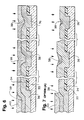
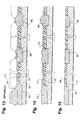
- Figs. 10-12 a second variation is shown for completing the process set forth in connection with figures 1-6.
- the next step (which pertains only to the wider trench) is to strip off the filler resist 40, as depicted in Fig. 10.
- the filler resist 40 may be stripped off using conventional methods, such as through the application of sulfuric acid plus hydrogen peroxide (H 2 0 2 ).
Landscapes
- Element Separation (AREA)
Applications Claiming Priority (2)
| Application Number | Priority Date | Filing Date | Title |
|---|---|---|---|
| US97587192A | 1992-11-13 | 1992-11-13 | |
| US975871 | 1992-11-13 |
Publications (2)
| Publication Number | Publication Date |
|---|---|
| EP0597603A2 true EP0597603A2 (fr) | 1994-05-18 |
| EP0597603A3 EP0597603A3 (fr) | 1998-03-11 |
Family
ID=25523513
Family Applications (1)
| Application Number | Title | Priority Date | Filing Date |
|---|---|---|---|
| EP93308495A Withdrawn EP0597603A3 (fr) | 1992-11-13 | 1993-10-25 | Planarisation d'une ramure d'isolation utilisant un masque dur |
Country Status (1)
| Country | Link |
|---|---|
| EP (1) | EP0597603A3 (fr) |
Cited By (4)
| Publication number | Priority date | Publication date | Assignee | Title |
|---|---|---|---|---|
| EP0637065A3 (fr) * | 1993-07-28 | 1995-05-03 | Digital Equipment Corp | Planarisation mécano-chimique de rainures plates sur substrates semi-conducteur. |
| WO1997006556A1 (fr) * | 1995-08-04 | 1997-02-20 | Siemens Aktiengesellschaft | Procede de production d'une couche d'espacement dans une structure |
| WO1997039479A1 (fr) * | 1996-04-17 | 1997-10-23 | Advanced Micro Devices, Inc. | Procede pour former des dielectriques a zones de champs de semiconducteurs comportant des surfaces superieures globalement planes |
| CN114127895A (zh) * | 2019-06-12 | 2022-03-01 | 东京毅力科创株式会社 | 半导体器件的平坦化 |
Family Cites Families (3)
| Publication number | Priority date | Publication date | Assignee | Title |
|---|---|---|---|---|
| US4962064A (en) * | 1988-05-12 | 1990-10-09 | Advanced Micro Devices, Inc. | Method of planarization of topologies in integrated circuit structures |
| US4962063A (en) * | 1988-11-10 | 1990-10-09 | Applied Materials, Inc. | Multistep planarized chemical vapor deposition process with the use of low melting inorganic material for flowing while depositing |
| DE69004932T2 (de) * | 1989-10-25 | 1994-05-19 | Ibm | Verfahren zur Herstellung breiter mit Dielektrikum gefüllter Isolationsgraben für Halbleiteranordnungen. |
-
1993
- 1993-10-25 EP EP93308495A patent/EP0597603A3/fr not_active Withdrawn
Cited By (7)
| Publication number | Priority date | Publication date | Assignee | Title |
|---|---|---|---|---|
| EP0637065A3 (fr) * | 1993-07-28 | 1995-05-03 | Digital Equipment Corp | Planarisation mécano-chimique de rainures plates sur substrates semi-conducteur. |
| US5494857A (en) * | 1993-07-28 | 1996-02-27 | Digital Equipment Corporation | Chemical mechanical planarization of shallow trenches in semiconductor substrates |
| WO1997006556A1 (fr) * | 1995-08-04 | 1997-02-20 | Siemens Aktiengesellschaft | Procede de production d'une couche d'espacement dans une structure |
| US6030900A (en) * | 1995-08-04 | 2000-02-29 | Siemens Aktiengesellschaft | Process for generating a space in a structure |
| WO1997039479A1 (fr) * | 1996-04-17 | 1997-10-23 | Advanced Micro Devices, Inc. | Procede pour former des dielectriques a zones de champs de semiconducteurs comportant des surfaces superieures globalement planes |
| US5830773A (en) * | 1996-04-17 | 1998-11-03 | Advanced Micro Devices, Inc. | Method for forming semiconductor field region dielectrics having globally planarized upper surfaces |
| CN114127895A (zh) * | 2019-06-12 | 2022-03-01 | 东京毅力科创株式会社 | 半导体器件的平坦化 |
Also Published As
| Publication number | Publication date |
|---|---|
| EP0597603A3 (fr) | 1998-03-11 |
Similar Documents
| Publication | Publication Date | Title |
|---|---|---|
| EP0545263B1 (fr) | Procédé pour former une rainure d'isolation comportant une étape de polissage et procédé pour fabriquer un dispositif semi-conducteur | |
| US7531415B2 (en) | Multilayered CMP stop for flat planarization | |
| US5753967A (en) | Damascene process for reduced feature size | |
| EP0284840B1 (fr) | Procédé pour former des couches uniformes de matériaux | |
| US7018906B2 (en) | Chemical mechanical polishing for forming a shallow trench isolation structure | |
| US5516625A (en) | Fill and etchback process using dual photoresist sacrificial layer and two-step etching process for planarizing oxide-filled shallow trench structure | |
| JPH0799237A (ja) | 集積回路の製造方法 | |
| US6017803A (en) | Method to prevent dishing in chemical mechanical polishing | |
| US5885900A (en) | Method of global planarization in fabricating integrated circuit devices | |
| US5750433A (en) | Methods of forming electrically isolated active region pedestals using trench-based isolation techniques | |
| US5217919A (en) | Method of forming island with polysilicon-filled trench isolation | |
| US5958795A (en) | Chemical-mechanical polishing for shallow trench isolation | |
| US6197691B1 (en) | Shallow trench isolation process | |
| US20020004284A1 (en) | Method for forming a shallow trench isolation structure including a dummy pattern in the wider trench | |
| US20020094649A1 (en) | Shallow trench isolation using non-conformal dielectric material and planarizatrion | |
| JP3302142B2 (ja) | 半導体装置の製造方法 | |
| US6376378B1 (en) | Polishing apparatus and method for forming an integrated circuit | |
| US6214695B1 (en) | Method of manufacturing semiconductor device | |
| US5830773A (en) | Method for forming semiconductor field region dielectrics having globally planarized upper surfaces | |
| US6242322B1 (en) | Method for forming shallow trench isolation filled with high-density plasma oxide layer | |
| EP0597603A2 (fr) | Planarisation d'une ramure d'isolation utilisant un masque dur | |
| US6443809B1 (en) | Polishing apparatus and method for forming an integrated circuit | |
| US20050032328A1 (en) | Chemical mechanical polishing in forming semiconductor device | |
| JP3274324B2 (ja) | 半導体装置の製造方法 | |
| US6403496B2 (en) | Method for forming shallow trench isolations |
Legal Events
| Date | Code | Title | Description |
|---|---|---|---|
| PUAI | Public reference made under article 153(3) epc to a published international application that has entered the european phase |
Free format text: ORIGINAL CODE: 0009012 |
|
| AK | Designated contracting states |
Kind code of ref document: A2 Designated state(s): DE FR GB IT |
|
| PUAL | Search report despatched |
Free format text: ORIGINAL CODE: 0009013 |
|
| AK | Designated contracting states |
Kind code of ref document: A3 Designated state(s): DE FR GB IT |
|
| 17P | Request for examination filed |
Effective date: 19980328 |
|
| 17Q | First examination report despatched |
Effective date: 19981113 |
|
| 18D | Application deemed to be withdrawn |
Effective date: 19990526 |