EP0597733B1 - Dispositif de codage d'images - Google Patents
Dispositif de codage d'images Download PDFInfo
- Publication number
- EP0597733B1 EP0597733B1 EP93309093A EP93309093A EP0597733B1 EP 0597733 B1 EP0597733 B1 EP 0597733B1 EP 93309093 A EP93309093 A EP 93309093A EP 93309093 A EP93309093 A EP 93309093A EP 0597733 B1 EP0597733 B1 EP 0597733B1
- Authority
- EP
- European Patent Office
- Prior art keywords
- data
- carry
- code
- over
- latch
- Prior art date
- Legal status (The legal status is an assumption and is not a legal conclusion. Google has not performed a legal analysis and makes no representation as to the accuracy of the status listed.)
- Expired - Lifetime
Links
Images


Classifications
-
- H—ELECTRICITY
- H04—ELECTRIC COMMUNICATION TECHNIQUE
- H04N—PICTORIAL COMMUNICATION, e.g. TELEVISION
- H04N1/00—Scanning, transmission or reproduction of documents or the like, e.g. facsimile transmission; Details thereof
- H04N1/41—Bandwidth or redundancy reduction
- H04N1/411—Bandwidth or redundancy reduction for the transmission or storage or reproduction of two-tone pictures, e.g. black and white pictures
- H04N1/413—Systems or arrangements allowing the picture to be reproduced without loss or modification of picture-information
- H04N1/417—Systems or arrangements allowing the picture to be reproduced without loss or modification of picture-information using predictive or differential encoding
-
- H—ELECTRICITY
- H03—ELECTRONIC CIRCUITRY
- H03M—CODING; DECODING; CODE CONVERSION IN GENERAL
- H03M7/00—Conversion of a code where information is represented by a given sequence or number of digits to a code where the same, similar or subset of information is represented by a different sequence or number of digits
- H03M7/30—Compression; Expansion; Suppression of unnecessary data, e.g. redundancy reduction
- H03M7/40—Conversion to or from variable length codes, e.g. Shannon-Fano code, Huffman code, Morse code
- H03M7/4006—Conversion to or from arithmetic code
Definitions
- the present invention relates to an image encoding device for compression encoding of image data, and more particularly to an image encoding device for encoding image data utilizing arithmetic codes.
- the arithmetic codes are utilized for example for image compression by adapted prediction, as described in ISO/IEC (Committee Draft 11544) etc.
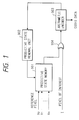
- Fig. 1 shows an example of the encoding circuit utilizing arithmetic codes.
- the binary data I of an object pixel to be encoded is supplied to an exclusive OR gate 904. Also the binary data X of plural reference pixels in the vicinity of the object pixel are supplied to a predictive state memory 901, which supplies the exclusive OR gate 904 with a predictive pixel data "0" or "1" according to the state of the reference pixel data.
- the exclusive OR gate 904 checks whether the object pixel data I coincides with the predictive pixel data from the predictive state memory 901, and supplies an arithmetic encoder 903 with the result.
- the arithmetic encoder 903 is provided with an interval size register (A register) indicating the current coding interval and a code register (C register), and shifts the values of said A and C registers according to the output of the exclusive OR gate 904. Then values of consecutive 8 bits in a specified position in said C register are outputted as encoded data.
- a register interval size register
- C register code register
- the content of the predictive state memory 901 is renewed according to an instruction of a prediction renewal unit 902, receiving the result of encoding, including the value of the A register of the arithmetic encoder 903. Consequently, the predictive state memory 901 supplies the exclusive OR gate 904 with the predictive pixel data adaptively to the current encoding operation.
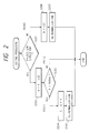
- Fig. 2 is a flow chart of the encoding operation of the encoder 903.
- a and C registers in the encoder 903 have a capacity of 32 bits each, and a section A is defined as 0 (0000H) - 0.5 (8000H) - 1.0 (10000H), wherein H stands for a hexadecimal number.
- the exclusive OR gate 904 compares the object pixel data with the predictive pixel data, and there is discriminated whether both data mutually coincide (S201). In case of coincidence, there is executed re-normalization shown in Fig. 4, and, in case of non-coincidence, there is executed re-normalization shown in Fig. 5.
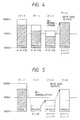
- Fig. 3 shows the sequence of re-normalization.
- the re-normalization shown in Fig. 3 is executed in case the object pixel data and the predictive pixel data do not mutually coincide, and also in case both data mutually coincide and the value A of the A register is less than 0.5 (8000H).
- the contents of said registers are shifted by a bit in the direction of MSB, and the count of a CT counter, counting the number of shifts, is decreased by "1" (S301).
- the data in a specified position of the C register are taken out as the encoded data at every eight shifts, in order to handle the encoded data as 8-bit parallel data.
- a value "8" is initially set in the CT counter, and said count is decreased stepwise at each 1-bit shift of the A register.
- the 8-bit encoded data are obtained when the count of the CT counter reaches "0".
- the sequence proceeds through a path 1 to add the value A of the A register to the value C of the C register (S204). Then, the re-normalization shown in Fig. 3 is executed in order to bring the value A, which is less than 0.5 (8000H) to a value equal to or larger than 0.5 (8000H), by shifting the A and C registers (S205). In this manner the contents of the A and C registers are renewed (phase 3 in Fig. 4). In this state, the count of the CT counter, counting the number of shifts of the A register, reaches "0", whereupon the upper byte of the C register is outputted as the encoded data.
- the sequence proceeds through a path 3 to define the value A of the A register as the constant LSZ (S206) and to execute the re-normalization shown in Fig. 3 by shifting the A register until the value A thereof becomes equal to or larger than 0.5 (8000H) (phases 1, 2, 3, 4 in Fig. 5).
- the A register is shifted three times. In this manner the content of the A register is renewed.
- the C register is also likewise shifted.
- the count of the CT counter reaches "0" at the first shift, whereupon the upper byte of the C register is outputted as the encoded data, and then the C register is set at "8".
- the value C shifted in the C register is outputted, in 8-bit unit, as the encoded data.
- Said value C is added, as shown in the step S204 in Fig. 2, to the value A. Consequently, the addition of a certain value C and a certain value A may result in a sum exceeding FFH. In such case, the carry-over will influence at least the preceding 8-bit encoded data. Consequently the 8-bit data from the C register cannot be directly supplied as the encoded data to the transmission channel or the like, and, if the addition of the values C and A may exceed FFH and may result in a carry-over, such carry-over has to be absorbed by a suitable method.
- Fig. 6 shows a circuit for the carry-over waiting method.
- the output a thereof is stored in a TEMP register 302.
- Said output a is a 9-bit data including carry-over.
- the output b of the TEMP register 302 is the carry-over bit, and the output c is an 8-bit data not including the carry-over bit.
- the output b is supplied to carry-over discrimination circuit 303, which releases an H (High) level or an L (Low) level in the output j respectively when the carry-over is present or absent.
- the output c is supplied to an FF discrimination circuit 304 for discriminating whether c is equal to FFH, and to a buffer register 305 for storing the output c.
- the FF discrimination circuit 304 releases a clock d for an increment of an SC counter 306 in case c is equal to FFH, and a clock e for storing c in the buffer register 305 in case c is not equal to FFH.
- the output of the arithmetic encoder 903 is stored in a TEMP register 302, and said stored value is assumed as BAH.
- BAH since the carry-over bit is not included, b is "0" and c is BAH. Consequently the carry-over discrimination circuit 303 releases an output "L", and the FF discrimination circuit 304 does not output the clock d for increment of the SC counter 306 but releases the clock e for storing the signal c in the buffer register 305.
- the count of the SC counter 306 is assumed as n, but same explanation can apply to any value of n equal to or larger than 0.
- the data of the C (Code) register are outputted in 8-bit (1 byte) unit or in carry-over bit + 8-bit unit and are stored in the TEMP register (S3). If the content of the TEMP register is smaller than FFH (S4), said content is stored in the buffer register. Since the next data to be outputted from the C register may result in a carry-over, the content of the buffer register is not outputted, but a waiting state is entered (S6).
- next data outputted from the C register and stored in the TEMP register is smaller than FFH, there is no longer the possibility of carry-over for the buffer register, so that the content of the buffer register is outputted as the encoded data, and the content of the TEMP register is newly fetched in the buffer register.
- the present invention is concerned with providing an image encoding device enabling real-time process in arithmetic encoding, and a method therefor.
- Another concern of the present invention is to provide an image encoding device capable of promptly and efficiently executing the carry-over process in the encoding utilizing arithmetic codes without influencing the preceding encoding, and a method therefor.
- Still another concern of the present invention is to provide an image encoding device capable of executing the above-mentioned carry-over process, without temporary interruption of the preceding encoding process, and a method therefor.
- an image encoding device as set out in claim 1.
- the present invention comprises an image encoding method as set out in claim 7.
- a 16-bit C register 201 there are provided a 16-bit C register 201; a 16-bit A register 202 for storing data indicating the current coding interval which is one of the parameters employed for encoding of image data; barrel shifters 203, 204 respectively for bit shift of the C register 201 and the A register 202; and a CT register 205 for retaining the CT value.
- a counter for subtraction there is employed a counter for subtraction, but, the present embodiment utilizes a register for retaining the entered CT value.
- a priority encoder 206 receives the outputs of the A register 202 and the CT register 205, controls the shifts of the barrel shifters 203, 204 and also controls a CT update logic 211 to renew the value of the CT register 205. It also controls a high-byte register 207 and a low-byte register 208 to control the output of the upper and lower bytes stored in the C register 201. There is also provided a carry-over control circuit 209.
- the content of the A register 202 is subjected, in a subtractor 212, to the subtraction of LSZ from an LSZ generator 213, and the result of said subtraction is supplied to a selector 214.
- Said selector 214 also receives the LSZ from the LSZ generator 214.
- the selector 214 selects either of the two inputs, according to the output of an exclusive OR gate 904, indicating coincidence or non-coincidence between the object pixel and the predictive pixel. More specifically, it selects the output (A - LSZ) from the subtractor 214 in case of coincidence, or the LSZ from the LSZ generator 213 in case of non-coincidence, and the selected signal is supplied to the A register 202 to renew the content thereof.
- the number of bits of shift can be uniquely determined according to the range of A, as shown in Fig. 10. This can be represented as "finding '1' in a bit position closest to the MSB side within the bits of A register".
- the above-mentioned bit position can be detected by a priority encoder 206 as shown in Fig. 9.
- the priority encoder 206 is composed of a logic circuit unit 509 and a 16 to 4 encoder 508.
- the bits stored in the A register 202 are taken out bit by bit in parallel manner, and supplied to the logic circuit unit 509 composed of inverters 502, 504, 506,... and AND gates 503, 505, 507,...
- the logic circuit unit 509 is so constructed that a high-level output signal is obtained only from an AND gate, among those 503, 505, 507,..., corresponding to '1' of the bit position closest to the MSB, among those stored in the A register 202.
- the high-level output signal is obtained only from the AND gate 503, corresponding to the 2nd bit, or MSB - 1, of the A register 202.
- the outputs of the AND gates 503, 505, 507,... are supplied to the 16-to-4 encoder 508, which releases 4-bit data indicating the bit position.
- Fig. 11 shows the structure of the barrel shifter 204 and the A register 202.
- the barrel shifter 203 and the C register 201 are also constructed in the same manner.
- 16-bit data stored in the A register 202 are supplied in parallel manner to the barrel shifter 204.
- the lower 15 bits of the barrel shifter 204 receive "0".
- Fig. 12 shows a correspondence table provided in the update logic 211. It will be understood that an output byte number of 0 to 2 can be obtained, depending on the number of shifts of 1 to 15 and the CT value of 1 to 8. These values are used, in an output control unit 210 shown in Fig. 8, for a control of no output for a value "0", the output of the codes of the high register 207 for a value "1”, and the output of two bytes of the high-byte register 207 and the low-byte register 208 for a value "2".
- the update logic 211 supplies the CT register 205 with a new CT value, which is retained therein.
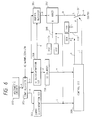
- Fig. 13 shows the structure of the carry-over control circuit 209 in Fig. 8, where in provided are flip-flops (F/F) 100 to 104, 110 to 114, 120 to 124 and 129; multiplexers or switches 105 to 109, 115 to 118 and 125 to 128; AND gates 131, 133, 134, 136, 137, 139, 140, 142 and 143; inverters 132, 135, 138, 141 and 144; a register 130 corresponding to the high-byte register 207 and the low-byte register 208 in Fig. 8; an adder 150; and an FF discrimination circuit 160.
- the broken-lined portion indicates repetition of similar circuits, consisting of serial connection of a required number of the circuit 170 framed in in a chain-lined frame.
- the register 130 releases a code train according to the above-explained encoding sequence and in synchronization with the re-normalization, wherein a is the carry-over data and b is data of at least a bit, excluding the carry-over.
- a is the carry-over data
- b is data of at least a bit, excluding the carry-over.
- the data b is assumed to be of 8 bits, as in the foregoing description.
- the flip-flops (F/F) 100 to 104, 110 to 114, 120 to 124 and 129 latch the input data in synchronization with the re-normalization. Consequently the data are shifted from left to right, at each re-normalization.
- the circuit 170 is assumed to be repeated 5 times so that the total number of shifts is five.
- code trains released from the register 130 at the re-normalizations are assumed to be C3H, BAH, FFH, FFH, 1AEH,...
- the flip-flops (F/F) 100 to 104 are reset.
- the register 130 releases an output C3H without carry-over, so that the output a is "0" and the output b is C3H.
- the output b is latched in the F/F 120.
- the FF discrimination circuit 160 for discriminating whether the output b is equal to FFH, upon receiving C3H, releases an output "0", which is latched in the F/F 100. Also since the output a is "0", the AND gate 131 releases an output "0" whereby the switch 109 is shifted to the L-side and the value "0" is latched in the F/F 110.
- the register 130 releases an output BAH, so that the output a is "0" and the output b is BAH.
- the F/F 100 releases an output "0”
- the F/F 110 releases an output "0”
- the F/F 120 releases an output BAH.
- the F/F 101 releases an output "0”
- the F/F 111 releases an output "0”
- the F/F 121 releases an output C3H.
- the register 130 releases an output FFH, so that the output a is "0" and the output b is FFH.
- the output b being FFH, is discriminated as equal to FFH in the FF discrimination circuit 160, which therefore releases an output "1", which is latched in the F/F 100.
- the F/F 129 releases an output C3H while the F/F 114 releases an output "0". Because there is no carry-over, the adder 150 releases an output C3H, which is outputted as established code output.
- the F/F 129 releases an output BAH while the F/F 114 releases an output "1". Because there is a carry-over, the adder 150 releases an output BBH, which is outputted as an established code output.
- the F/F 129 outputs 00H while the F/F 114 releases an output "0". Because there is no carry-over, the adder 150 releases an output 00H, which is outputted as the established code output.
- the F/F 129 releases an output 00H, while the F/F 114 releases an output "0". Since there is no carry-over, the adder 150 releases an output 00H, which is outputted as the established code output.
- the output of the arithmetic encoder is assumed to be based on positive logic, but a similar object can be attained naturally through negative logic.
- the logic circuit composed of the multiplexers (switches), AND gates and inverters is not limited to that shown in Fig. 13, but an equivalent function can be attained by other logic circuits.
- Fig. 14 shows another embodiment of the carry-over process circuit 209, wherein provided are flip-flops 410 to 414, 420 to 424 and 429; multiplexers or switches 409, 415 to 418, 425 to 428; AND gates 431, 433, 434, 436, 437, 439, 440, 441, 443 and 444; inverters 432, 435, 438, 442 and 445; a register 430 corresponding to the high-byte register 207 and the low-byte register 208 in Fig. 8; an adder 450; and FF discrimination circuits 460 to 464.
- the broken-lined portion indicates repetition of similar circuits, consisting of serial connection of a required number of the circuit 470 surrounded in a chain-lined frame.
- the FF discrimination circuit for discriminating whether the output data of the register 430 is FFH, is provided at each output of the flip-flops 421 to 424, and this difference will be clarified further in the following description based on the same assumptions and conditions as in the foregoing description.
- the register 430 releases an output C3H without the carry-over, so that the output a is "0" and the output b is C3H.
- the output b is latched in the F/F 420. Since the AND gate 431 releases an output "0”, the switch 409 is shifted to the L-side, and the F/F 410 latches "0".
- the register 430 releases an output BAH, so that the output a is "0" and the output b is BAH.
- the F/F 410 releases an output "0"
- the F/F 420 releases an output BAH.
- the F/F 411 releases an output "0”
- the F/F 421 releases an output C3H.
- the register 430 releases an output FFH, so that the output a is "0" and. the output b is FFH.
- the output a is "0" and. the output b is FFH.
- the register 430 releases an output lAEH including a carry-over, so that the output a is "1" and the output b is AEH.
- the F/F 429 releases an output C3H, while the F/F 414 releases an output "0". Since there is no carry-over, the adder 450 releases an output C3H, which is outputted as an established code output. Then, at the next re-normalization, the F/F 429 releases an output BAH while the F/F 414 releases an output "1". Since there is a carry-over, the adder 450 releases an output BBH, which is outputted as an established code output.
Landscapes
- Engineering & Computer Science (AREA)
- Theoretical Computer Science (AREA)
- Multimedia (AREA)
- Signal Processing (AREA)
- Compression, Expansion, Code Conversion, And Decoders (AREA)
- Compression Or Coding Systems Of Tv Signals (AREA)
Claims (13)
- Dispositif de codage d'image comprenant:caractérisé en ce que :des moyens de codage (201-216) pour coder des données d'image sur la base d'un code arithmétique afin d'engendrer des données de code composées de "0" et de "1";des moyens de sortie (130; 430) pour produire en sortie les données de code et des données de report indiquant un report; etun moyen de processus de report (209) pour effectuer un processus de report sur les données de code conformément aux données de report,ledit moyen de processus de report (209) comprend:lesdits moyens de sortie (130; 430) produisent en sortie les données de code en tant que nombre prédéterminé de bits en parallèle ainsi que des données de report d'un seul bit lequel bit unique indique qu'il y a ou qu'il n'y a pas de report,une pluralité de moyens à verrouillage de code connectés en série (120-124; 420-424) dont chacun verrouille les données de code du nombre prédéterminé de bits, les données de code du nombre prédéterminé de bits étant décalées en parallèle par l'intermédiaire de ladite pluralité de moyens à verrouillage de code;une pluralité de moyens à verrouillage de données connectés en série (110-114; 410-414) dont chacun verrouille les données de report de bit unique correspondant à chacun de ladite pluralité de moyens à verrouillage de code, le bit unique des données de report étant décalé par l'intermédiaire de ladite pluralité de moyens à verrouillage de données en synchronisme avec le décalage en parallèle des données de code du nombre prédéterminé de bits par l'intermédiaire de la pluralité de moyens à verrouillage de code; etdes moyens d'addition (150; 450) pour additionner le bit unique de données de report qui a été décalé par l'intermédiaire de ladite pluralité de moyens à verrouillage de données et les données de code du nombre prédéterminé de bits décalées en parallèle par l'intermédiaire de ladite pluralité de moyens à verrouillage de code, afin de produire en sortie un résultat de l'addition comme étant des données de code établies.
- Dispositif selon la revendication 1, dans lequel le bit unique de données de report indique qu'il y a un report lorsque le bit est "1".
- Dispositif selon la revendication 2, dans lequel, dans le cas où les données de report sont produites à partir desdits moyens de sortie après que les données de code dont tous les bits sont des "1" sont produites à partir desdits moyens de sortie et sont verrouillées dans un premier étage desdits moyens à verrouillage de code, ledit moyen de processus de report permet à un deuxième étage desdits moyens à verrouillage de données de code de verrouiller les données de code dont tous les bits sont des "0" et permet auxdits moyens à verrouillage de données correspondant au deuxième étage desdits moyens à verrouillage de code de verrouiller les données de report.
- Dispositif selon la revendication 2, dans lequel, dans le cas où les données de report sont verrouillées dans lesdits moyens à verrouillage de données correspondant auxdits moyens à verrouillage de code avant lesdits moyens à verrouillage de code qui verrouillent les données de code dont tous les bits sont des "1", ledit moyen de processus de report permet à un étage suivant desdits moyens à verrouillage de code de verrouiller les données de code dont tous les bits sont des "0" et permet auxdits moyens à verrouillage de données correspondant à l'étage suivant desdits moyens à verrouillage de code de verrouiller les données de report.
- Dispositif selon la revendication 3 ou 4, comprenant en outre des moyens de détermination pour déterminer si tous les bits des données de code verrouillées dans chacun de ladite pluralité de moyens à verrouillage de code, sont, ou non, des "1".
- Dispositif selon la revendication 5, dans lequel ledit moyen de processus de report effectue le processus de report sur des données de code dont tous les bits sont des "1" conformément au résultat de détermination desdits moyens de détermination.
- Procédé de codage d'image comprenant:caractérisé en ce que :une étape de codage pour coder des données d'image sur la base d'un code arithmétique afin d'engendrer des données de code composées de "0" et de "1".une étape de sortie pour produire en sortie les données de code et des données de report indiquant un report; etune étape de processus de report pour effectuer un processus de report sur les données de code conformément aux données de report,ladite étape de processus de report comprend:ladite étape de sortie produit en sortie les données de code en tant que nombre prédéterminé de bits en parallèle et des données de report sous la forme d'un bit unique qui indique s'il y a, ou non, un report,une première étape de décalage pour décaler en parallèle les données de code du nombre prédéterminé de bits par l'intermédiaire d'une pluralité de dispositifs à verrouillage de code connectés en série dont chacun verrouille les données de code du nombre prédéterminé de bits;une deuxième étape de décalage pour décaler les données de report de un bit par l'intermédiaire d'une pluralité de dispositifs à verrouillage de données connectés en série en synchronisme avec le décalage en parallèle des données de code du nombre prédéterminé de bits par l'intermédiaire de la pluralité de dispositifs à verrouillage de code, chacun des dispositifs à verrouillage de données verrouillant les données de report de un bit; etune étape supplémentaire pour additionner les données de report décalées de un bit par l'intermédiaire de la pluralité de dispositifs à verrouillage de données et les données de code du nombre prédéterminé de bits décalées en parallèle par l'intermédiaire de la pluralité de dispositifs à verrouillage de code, afin de produire en sortie un résultat de l'addition comme étant des données de code établies.
- Procédé selon la revendication 7, dans lequel le bit unique de report est "1" lorsqu'il indique qu'il y a un report.
- Procédé selon la revendication 7, dans lequel ladite étape de processus de report effectue un processus de report sur les données de code verrouillées dans la pluralité de dispositifs à verrouillage de données de code conformément aux données de report.
- Procédé selon la revendication 9 dans lequel, dans un cas où les données de report sont produites en sortie dans ladite étape de sortie après que les données de code dont tous les bits sont des "1" sont produites dans ladite étape de sortie et sont verrouillées dans un premier étage du dispositif à verrouillage de code, ladite étape de processus de report permet à un deuxième étage du dispositif à verrouillage de données de code de verrouiller les données de code dont tous les bits sont des "0" et permet au dispositif à verrouillage de données correspondant au deuxième étage du dispositif à verrouillage de code de verrouiller les données de report.
- Procédé selon la revendication 9, dans lequel, dans un cas où les données de report sont verrouillées dans le dispositif à verrouillage de données correspondant au dispositif à verrouillage de code avant le dispositif à verrouillage de code qui verrouille les données de code dont tous les bits sont des "1", ladite étape de processus de report permet à un étage suivant du dispositif à verrouillage de code de verrouiller les données de code dont tous les bits sont des "0" et permet au dispositif à verrouillage de données correspondant à l'étage suivant du dispositif à verrouillage de code de verrouiller les données de report.
- Procédé selon la revendication 10 ou 11, comprenant en outre une étape de détermination pour déterminer si tous les bits des données de code verrouillées dans chacun de la pluralité de dispositifs à verrouillage de code, sont, ou non, des "1".
- Procédé selon la revendication 12, dans lequel ladite étape de processus de report effectue le processus de report sur les données de code dont tous les bits sont des "1" conformément au résultat de détermination de ladite étape de détermination.
Applications Claiming Priority (2)
| Application Number | Priority Date | Filing Date | Title |
|---|---|---|---|
| JP303932/92 | 1992-11-13 | ||
| JP30393292 | 1992-11-13 |
Publications (2)
| Publication Number | Publication Date |
|---|---|
| EP0597733A1 EP0597733A1 (fr) | 1994-05-18 |
| EP0597733B1 true EP0597733B1 (fr) | 1998-08-05 |
Family
ID=17927022
Family Applications (1)
| Application Number | Title | Priority Date | Filing Date |
|---|---|---|---|
| EP93309093A Expired - Lifetime EP0597733B1 (fr) | 1992-11-13 | 1993-11-12 | Dispositif de codage d'images |
Country Status (3)
| Country | Link |
|---|---|
| US (1) | US5784497A (fr) |
| EP (1) | EP0597733B1 (fr) |
| DE (1) | DE69320147T2 (fr) |
Families Citing this family (9)
| Publication number | Priority date | Publication date | Assignee | Title |
|---|---|---|---|---|
| JP3409552B2 (ja) * | 1995-12-27 | 2003-05-26 | 三菱電機株式会社 | ディジタル情報符号化装置、ディジタル情報復号化装置、及びディジタル情報符号化・復号化装置 |
| CN1178458C (zh) * | 1996-07-31 | 2004-12-01 | 松下电器产业株式会社 | 图象解码装置和图象解码方法 |
| US6055338A (en) * | 1996-08-22 | 2000-04-25 | Sumitomo Metal Industries Limited | Bi-level adaptive coding using a dual port memory and a context comparator |
| US6058216A (en) * | 1996-09-03 | 2000-05-02 | Sumitomo Metal Industries Limited | Apparatus for encoding image data |
| JPH1093827A (ja) * | 1996-09-11 | 1998-04-10 | Canon Inc | 画像処理方法とその装置 |
| JP3185769B2 (ja) * | 1998-10-26 | 2001-07-11 | 日本電気株式会社 | 画像信号処理装置 |
| US6313767B1 (en) | 1999-02-19 | 2001-11-06 | Canon Kabushiki Kaisha | Decoding apparatus and method |
| JP3853710B2 (ja) * | 2002-07-15 | 2006-12-06 | Necアクセステクニカ株式会社 | ディジタル画像符号化装置およびディジタル画像符号化方法 |
| US7236633B1 (en) * | 2003-03-21 | 2007-06-26 | Altera Corporation | Data compression and decompression techniques for programmable circuits |
Family Cites Families (11)
| Publication number | Priority date | Publication date | Assignee | Title |
|---|---|---|---|---|
| US4463342A (en) * | 1979-06-14 | 1984-07-31 | International Business Machines Corporation | Method and means for carry-over control in the high order to low order pairwise combining of digits of a decodable set of relatively shifted finite number strings |
| US4286256A (en) * | 1979-11-28 | 1981-08-25 | International Business Machines Corporation | Method and means for arithmetic coding utilizing a reduced number of operations |
| US4467317A (en) * | 1981-03-30 | 1984-08-21 | International Business Machines Corporation | High-speed arithmetic compression coding using concurrent value updating |
| US4905297A (en) * | 1986-09-15 | 1990-02-27 | International Business Machines Corporation | Arithmetic coding encoder and decoder system |
| US4891643A (en) * | 1986-09-15 | 1990-01-02 | International Business Machines Corporation | Arithmetic coding data compression/de-compression by selectively employed, diverse arithmetic coding encoders and decoders |
| US4870695A (en) * | 1987-03-20 | 1989-09-26 | International Business Machines Corporation | Compression and de-compression of column-interlaced, row-interlaced graylevel digital images |
| JP2672521B2 (ja) * | 1987-09-21 | 1997-11-05 | 株式会社東芝 | 画像処理方法 |
| US4973961A (en) * | 1990-02-12 | 1990-11-27 | At&T Bell Laboratories | Method and apparatus for carry-over control in arithmetic entropy coding |
| US5262873A (en) * | 1990-11-07 | 1993-11-16 | Canon Kabushiki Kaisha | Image signal correcting in image data processing requiring only small memory capacity |
| US5298896A (en) * | 1993-03-15 | 1994-03-29 | Bell Communications Research, Inc. | Method and system for high order conditional entropy coding |
| JP2836467B2 (ja) * | 1993-12-16 | 1998-12-14 | 日本電気株式会社 | 2値シンボルの符号化・復号化回路 |
-
1993
- 1993-11-12 EP EP93309093A patent/EP0597733B1/fr not_active Expired - Lifetime
- 1993-11-12 DE DE69320147T patent/DE69320147T2/de not_active Expired - Fee Related
-
1996
- 1996-03-06 US US08/611,497 patent/US5784497A/en not_active Expired - Fee Related
Also Published As
| Publication number | Publication date |
|---|---|
| US5784497A (en) | 1998-07-21 |
| DE69320147D1 (de) | 1998-09-10 |
| EP0597733A1 (fr) | 1994-05-18 |
| DE69320147T2 (de) | 1999-01-14 |
Similar Documents
| Publication | Publication Date | Title |
|---|---|---|
| US6014095A (en) | Variable length encoding system | |
| US4463342A (en) | Method and means for carry-over control in the high order to low order pairwise combining of digits of a decodable set of relatively shifted finite number strings | |
| EP1014589A2 (fr) | Décodeur pour mots de code à longueur variable | |
| EP0245621B1 (fr) | Compression des signaux à plusieurs niveaux | |
| US4486784A (en) | Image compression systems | |
| JPH07177039A (ja) | ハフマン符号化復号化装置 | |
| EP0510627B1 (fr) | Dispositifs de codage et de décodage | |
| US5115241A (en) | Predictive coding device with increased resolution | |
| EP0597733B1 (fr) | Dispositif de codage d'images | |
| US6408102B1 (en) | Encoding/decoding device | |
| JPH053950B2 (fr) | ||
| EP0260461B1 (fr) | Méthode de codage arithmétique pour codage et décodage | |
| EP0581571B1 (fr) | Dispositif et procédé pour le codage d'images | |
| US3984833A (en) | Apparatus for encoding extended run-length codes | |
| US5532949A (en) | Barrel shifter | |
| JP3459759B2 (ja) | 算術復号化装置 | |
| JP3219571B2 (ja) | 画像符号化装置及び方法 | |
| JP3184670B2 (ja) | 画像符号化装置 | |
| US6058216A (en) | Apparatus for encoding image data | |
| US5062125A (en) | Statistic coding arrangement for producing code words comprising a variable number of bits | |
| KR100292050B1 (ko) | 가변장복호기의 데이타 가변장치 | |
| US20020057742A1 (en) | Sorting device of variable-length code | |
| JP3595659B2 (ja) | パッキング回路 | |
| JPH04270569A (ja) | 画像処理装置におけるデータ圧縮方式 | |
| JP2000278538A (ja) | 算術符号化・復号化装置および方法 |
Legal Events
| Date | Code | Title | Description |
|---|---|---|---|
| PUAI | Public reference made under article 153(3) epc to a published international application that has entered the european phase |
Free format text: ORIGINAL CODE: 0009012 |
|
| AK | Designated contracting states |
Kind code of ref document: A1 Designated state(s): DE FR GB IT NL |
|
| 17P | Request for examination filed |
Effective date: 19940930 |
|
| 17Q | First examination report despatched |
Effective date: 19961008 |
|
| GRAG | Despatch of communication of intention to grant |
Free format text: ORIGINAL CODE: EPIDOS AGRA |
|
| GRAG | Despatch of communication of intention to grant |
Free format text: ORIGINAL CODE: EPIDOS AGRA |
|
| GRAH | Despatch of communication of intention to grant a patent |
Free format text: ORIGINAL CODE: EPIDOS IGRA |
|
| GRAH | Despatch of communication of intention to grant a patent |
Free format text: ORIGINAL CODE: EPIDOS IGRA |
|
| GRAA | (expected) grant |
Free format text: ORIGINAL CODE: 0009210 |
|
| AK | Designated contracting states |
Kind code of ref document: B1 Designated state(s): DE FR GB IT NL |
|
| PG25 | Lapsed in a contracting state [announced via postgrant information from national office to epo] |
Ref country code: NL Free format text: LAPSE BECAUSE OF FAILURE TO SUBMIT A TRANSLATION OF THE DESCRIPTION OR TO PAY THE FEE WITHIN THE PRESCRIBED TIME-LIMIT Effective date: 19980805 Ref country code: IT Free format text: LAPSE BECAUSE OF FAILURE TO SUBMIT A TRANSLATION OF THE DESCRIPTION OR TO PAY THE FEE WITHIN THE PRESCRIBED TIME-LIMIT;WARNING: LAPSES OF ITALIAN PATENTS WITH EFFECTIVE DATE BEFORE 2007 MAY HAVE OCCURRED AT ANY TIME BEFORE 2007. THE CORRECT EFFECTIVE DATE MAY BE DIFFERENT FROM THE ONE RECORDED. Effective date: 19980805 |
|
| REF | Corresponds to: |
Ref document number: 69320147 Country of ref document: DE Date of ref document: 19980910 |
|
| ET | Fr: translation filed | ||
| NLV1 | Nl: lapsed or annulled due to failure to fulfill the requirements of art. 29p and 29m of the patents act | ||
| PLBE | No opposition filed within time limit |
Free format text: ORIGINAL CODE: 0009261 |
|
| 26N | No opposition filed | ||
| REG | Reference to a national code |
Ref country code: GB Ref legal event code: IF02 |
|
| PGFP | Annual fee paid to national office [announced via postgrant information from national office to epo] |
Ref country code: DE Payment date: 20071130 Year of fee payment: 15 |
|
| PGFP | Annual fee paid to national office [announced via postgrant information from national office to epo] |
Ref country code: GB Payment date: 20071112 Year of fee payment: 15 Ref country code: FR Payment date: 20071122 Year of fee payment: 15 |
|
| GBPC | Gb: european patent ceased through non-payment of renewal fee |
Effective date: 20081112 |
|
| REG | Reference to a national code |
Ref country code: FR Ref legal event code: ST Effective date: 20090731 |
|
| PG25 | Lapsed in a contracting state [announced via postgrant information from national office to epo] |
Ref country code: DE Free format text: LAPSE BECAUSE OF NON-PAYMENT OF DUE FEES Effective date: 20090603 |
|
| PG25 | Lapsed in a contracting state [announced via postgrant information from national office to epo] |
Ref country code: GB Free format text: LAPSE BECAUSE OF NON-PAYMENT OF DUE FEES Effective date: 20081112 |
|
| PG25 | Lapsed in a contracting state [announced via postgrant information from national office to epo] |
Ref country code: FR Free format text: LAPSE BECAUSE OF NON-PAYMENT OF DUE FEES Effective date: 20081130 |