EP0598308A1 - Differential-Komparatorschaltung - Google Patents
Differential-Komparatorschaltung Download PDFInfo
- Publication number
- EP0598308A1 EP0598308A1 EP93118119A EP93118119A EP0598308A1 EP 0598308 A1 EP0598308 A1 EP 0598308A1 EP 93118119 A EP93118119 A EP 93118119A EP 93118119 A EP93118119 A EP 93118119A EP 0598308 A1 EP0598308 A1 EP 0598308A1
- Authority
- EP
- European Patent Office
- Prior art keywords
- transistor
- transistors
- volts
- gate
- signal
- Prior art date
- Legal status (The legal status is an assumption and is not a legal conclusion. Google has not performed a legal analysis and makes no representation as to the accuracy of the status listed.)
- Granted
Links
- 230000008878 coupling Effects 0.000 claims description 4
- 238000010168 coupling process Methods 0.000 claims description 4
- 238000005859 coupling reaction Methods 0.000 claims description 4
- 238000006880 cross-coupling reaction Methods 0.000 abstract 1
- 239000004973 liquid crystal related substance Substances 0.000 description 22
- 239000003990 capacitor Substances 0.000 description 18
- 238000005070 sampling Methods 0.000 description 12
- 230000005540 biological transmission Effects 0.000 description 11
- 229910021417 amorphous silicon Inorganic materials 0.000 description 6
- 210000002858 crystal cell Anatomy 0.000 description 6
- 239000004020 conductor Substances 0.000 description 5
- 230000001143 conditioned effect Effects 0.000 description 4
- 238000010586 diagram Methods 0.000 description 3
- 238000005516 engineering process Methods 0.000 description 3
- 239000000463 material Substances 0.000 description 3
- 239000010409 thin film Substances 0.000 description 2
- 230000000295 complement effect Effects 0.000 description 1
- 230000000694 effects Effects 0.000 description 1
- 230000005669 field effect Effects 0.000 description 1
- 238000004519 manufacturing process Methods 0.000 description 1
- 239000011159 matrix material Substances 0.000 description 1
- 230000003071 parasitic effect Effects 0.000 description 1
- 239000000758 substrate Substances 0.000 description 1
Images


Classifications
-
- H—ELECTRICITY
- H03—ELECTRONIC CIRCUITRY
- H03K—PULSE TECHNIQUE
- H03K3/00—Circuits for generating electric pulses; Monostable, bistable or multistable circuits
-
- G—PHYSICS
- G09—EDUCATION; CRYPTOGRAPHY; DISPLAY; ADVERTISING; SEALS
- G09G—ARRANGEMENTS OR CIRCUITS FOR CONTROL OF INDICATING DEVICES USING STATIC MEANS TO PRESENT VARIABLE INFORMATION
- G09G3/00—Control arrangements or circuits, of interest only in connection with visual indicators other than cathode-ray tubes
- G09G3/20—Control arrangements or circuits, of interest only in connection with visual indicators other than cathode-ray tubes for presentation of an assembly of a number of characters, e.g. a page, by composing the assembly by combination of individual elements arranged in a matrix no fixed position being assigned to or needed to be assigned to the individual characters or partial characters
- G09G3/2007—Display of intermediate tones
- G09G3/2011—Display of intermediate tones by amplitude modulation
-
- G—PHYSICS
- G09—EDUCATION; CRYPTOGRAPHY; DISPLAY; ADVERTISING; SEALS
- G09G—ARRANGEMENTS OR CIRCUITS FOR CONTROL OF INDICATING DEVICES USING STATIC MEANS TO PRESENT VARIABLE INFORMATION
- G09G3/00—Control arrangements or circuits, of interest only in connection with visual indicators other than cathode-ray tubes
- G09G3/20—Control arrangements or circuits, of interest only in connection with visual indicators other than cathode-ray tubes for presentation of an assembly of a number of characters, e.g. a page, by composing the assembly by combination of individual elements arranged in a matrix no fixed position being assigned to or needed to be assigned to the individual characters or partial characters
- G09G3/34—Control arrangements or circuits, of interest only in connection with visual indicators other than cathode-ray tubes for presentation of an assembly of a number of characters, e.g. a page, by composing the assembly by combination of individual elements arranged in a matrix no fixed position being assigned to or needed to be assigned to the individual characters or partial characters by control of light from an independent source
- G09G3/36—Control arrangements or circuits, of interest only in connection with visual indicators other than cathode-ray tubes for presentation of an assembly of a number of characters, e.g. a page, by composing the assembly by combination of individual elements arranged in a matrix no fixed position being assigned to or needed to be assigned to the individual characters or partial characters by control of light from an independent source using liquid crystals
- G09G3/3611—Control of matrices with row and column drivers
- G09G3/3685—Details of drivers for data electrodes
- G09G3/3688—Details of drivers for data electrodes suitable for active matrices only
-
- H—ELECTRICITY
- H03—ELECTRONIC CIRCUITRY
- H03F—AMPLIFIERS
- H03F3/00—Amplifiers with only discharge tubes or only semiconductor devices as amplifying elements
- H03F3/45—Differential amplifiers
- H03F3/45071—Differential amplifiers with semiconductor devices only
- H03F3/45076—Differential amplifiers with semiconductor devices only characterised by the way of implementation of the active amplifying circuit in the differential amplifier
-
- H—ELECTRICITY
- H03—ELECTRONIC CIRCUITRY
- H03K—PULSE TECHNIQUE
- H03K5/00—Manipulating of pulses not covered by one of the other main groups of this subclass
- H03K5/22—Circuits having more than one input and one output for comparing pulses or pulse trains with each other according to input signal characteristics, e.g. slope, integral
- H03K5/24—Circuits having more than one input and one output for comparing pulses or pulse trains with each other according to input signal characteristics, e.g. slope, integral the characteristic being amplitude
- H03K5/2472—Circuits having more than one input and one output for comparing pulses or pulse trains with each other according to input signal characteristics, e.g. slope, integral the characteristic being amplitude using field effect transistors
- H03K5/249—Circuits having more than one input and one output for comparing pulses or pulse trains with each other according to input signal characteristics, e.g. slope, integral the characteristic being amplitude using field effect transistors using clock signals
-
- G—PHYSICS
- G09—EDUCATION; CRYPTOGRAPHY; DISPLAY; ADVERTISING; SEALS
- G09G—ARRANGEMENTS OR CIRCUITS FOR CONTROL OF INDICATING DEVICES USING STATIC MEANS TO PRESENT VARIABLE INFORMATION
- G09G2310/00—Command of the display device
- G09G2310/02—Addressing, scanning or driving the display screen or processing steps related thereto
- G09G2310/0243—Details of the generation of driving signals
- G09G2310/0259—Details of the generation of driving signals with use of an analog or digital ramp generator in the column driver or in the pixel circuit
Definitions
- the input stage of a standard differential amplifier comparator formed using insulated-gate field-effect transistors normally includes first and second IGFETs having their source electrodes connected in common to a common current source and with an input signal applied to the gate of the first IGFET and a reference signal applied to the gate of the second IGFET.
- IGFETs insulated-gate field-effect transistors
- the threshold voltages i.e. the gate-to-source voltages, VGS, at low source-to-drain current
- the input signal will appear to be greater or smaller than it actually is, resulting in an error.
- TFTs thin film transistors
- IGFETs thin film transistors
- the threshold voltages of TFTs or IGFETs made of amorphous silicon tend to be non-uniform due to processing and other factors and to shift or drift during operation when subjected to different stress potentials.
- amorphous silicon transistors would normally not be used to form a differential comparator.
- circuitry for driving liquid crystal displays Amorphous silicon is a desirable technology for fabricating liquid crystal displays because this material can be fabricated at low temperatures which permits the use of standard, readily available, and inexpensive substrate materials.
- the liquid crystal displays are normally composed of a matrix of pixels arranged in rows and columns. These pixels have to be driven by row and column drivers which are in turn driven by switching and control circuits. For purpose of economy of space and to reduce fabrication cost, it is preferable to simultaneously fabricate the control and switching circuitry driving the rows and columns of the liquid crystal display elements using the same technology used to form the liquid crystal display. Furthermore, it is desirable to form the control and switching circuitry around the periphery of the liquid crystal display at the same time as the liquid crystal display is formed. Therefore, there are compelling economic reasons (among others) for employing amorphous silicon transistors in the design of the control and switching circuitry including any comparator circuits.
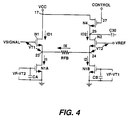
- a comparator circuit embodying the invention includes a first transistor adapted to receive an input signal at its gate electrode, a second transistor adapted to receive a reference signal at its gate electrode, a third transistor having its conduction path connected between the source electrodes of the first and second transistors, and a current source means arranged to be selectively cross coupled across the third transistor to provide and autobalance bias current conducted by said first and second transistors.
- Circuits and systems embodying the invention may be formed using transistors made of amorphous silicon which have low mobility, low gain and non-uniform threshold voltages which drift with time and voltage stress.
- the use of such transistors is dictated by the need to fabricate cost effective scanning circuits using the same material as the components of a liquid crystal display panel of the type shown as 160 in FIGURE 1 with which they are intended to operate. This feature enables the components of the system to be more easily integrated and manufactured more inexpensively.
- analog circuitry 110 receives an analog information signal representative of the data to be displayed from an antenna 120.
- the analog circuitry 110 is similar to that of a standard television receiver of known type. However, the tube is replaced by a liquid crystal display device as described herein.
- the analog circuitry 110 provides an analog data bearing signal on a line 130 as an input signal to an analog-to-digital converter (A/D) 140.
- A/D analog-to-digital converter
- the television signal from the analog circuitry 110 is to be displayed on a liquid crystal array 160 which is composed of a large number of pixel elements, such as the liquid crystal cell 160a, arranged horizontally in m rows and vertically in n columns.
- the liquid crystal array 160 includes n columns of data lines 38, one for each of the vertical columns of liquid crystal cells, and m select lines 180, one for each of the horizontal rows of liquid crystal cells.
- the A/D converter 140 includes an output bus 190 to provide brightness levels or gray scale codes, to a digital storage means 210 having a plurality of output lines 220.
- the output lines 220 of the digital storage means 210 control the voltages applied to the data lines 38 for the columns of liquid crystal cells 160a through digital-to-analog converters (D/A) 230, comparators 240 and transmission gates N5.
- D/A digital-to-analog converters
- comparators 240 comparators 240 and transmission gates N5.
- Each of the output lines 220 therefore controls the voltage applied to the liquid crystal cell in a particular column when an associated transmission gate N5 is conducting and in accordance with the scanning of the select lines 180.
- a display device using counters and a preferred embodiment of the digital storage means 210, in the form of a shift register, are described in U.S. Patent Nos.
- a reference ramp generator 330 provides a reference ramp voltage signal on an output line 270 which is coupled to the respective comparators 240 in each of the columns of liquid crystal cells via a line 26.
- a data ramp generator 340 provides a data ramp to the columns of pixel elements by the connection of an output line 37 to each of the transmission gates N5.
- the transmission gates N5 are thin film transistors which are coupled to the outputs of the comparators 240 by lines 31.
Landscapes
- Engineering & Computer Science (AREA)
- Physics & Mathematics (AREA)
- Theoretical Computer Science (AREA)
- Computer Hardware Design (AREA)
- General Physics & Mathematics (AREA)
- Nonlinear Science (AREA)
- Power Engineering (AREA)
- Chemical & Material Sciences (AREA)
- Crystallography & Structural Chemistry (AREA)
- Manipulation Of Pulses (AREA)
- Liquid Crystal Display Device Control (AREA)
- Control Of Indicators Other Than Cathode Ray Tubes (AREA)
- Stabilization Of Oscillater, Synchronisation, Frequency Synthesizers (AREA)
- Liquid Crystal (AREA)
Applications Claiming Priority (2)
| Application Number | Priority Date | Filing Date | Title |
|---|---|---|---|
| US976607 | 1992-11-16 | ||
| US07/976,607 US5352937A (en) | 1992-11-16 | 1992-11-16 | Differential comparator circuit |
Publications (2)
| Publication Number | Publication Date |
|---|---|
| EP0598308A1 true EP0598308A1 (de) | 1994-05-25 |
| EP0598308B1 EP0598308B1 (de) | 1996-09-18 |
Family
ID=25524273
Family Applications (1)
| Application Number | Title | Priority Date | Filing Date |
|---|---|---|---|
| EP93118119A Expired - Lifetime EP0598308B1 (de) | 1992-11-16 | 1993-11-09 | Differential-Komparatorschaltung |
Country Status (11)
| Country | Link |
|---|---|
| US (1) | US5352937A (de) |
| EP (1) | EP0598308B1 (de) |
| JP (1) | JPH06224710A (de) |
| KR (1) | KR940012824A (de) |
| CN (1) | CN1043105C (de) |
| DE (1) | DE69304867T2 (de) |
| ES (1) | ES2094449T3 (de) |
| HK (1) | HK1004306A1 (de) |
| MY (1) | MY111029A (de) |
| SG (1) | SG86967A1 (de) |
| TW (1) | TW228040B (de) |
Cited By (12)
| Publication number | Priority date | Publication date | Assignee | Title |
|---|---|---|---|---|
| EP0694900A3 (de) * | 1994-07-27 | 1996-04-10 | Sharp Kk | Anzeigeeinrichtung mit aktiver Matrix und Steuerverfahren dafür |
| EP0731439A1 (de) * | 1995-03-06 | 1996-09-11 | THOMSON multimedia | System zur Steuerung von Datenleitungen mit Helligkeitssignalen in eine Anzeige |
| EP0731440A1 (de) * | 1995-03-06 | 1996-09-11 | THOMSON multimedia | Treiberschaltungen für Datenleitungen mit einem gemeinsamen Rampensignal für ein Anzeigesystem |
| EP0777900A4 (de) * | 1994-08-31 | 1997-09-10 | Sarnoff David Res Center | Bildanzeigearchitektur |
| CN1043105C (zh) * | 1992-11-16 | 1999-04-21 | Rca汤姆森许可公司 | 差分比较器电路 |
| EP0961401A1 (de) * | 1998-05-29 | 1999-12-01 | Texas Instruments Incorporated | Pufferverstärker für niedrige Speisespannung |
| WO1999053619A3 (en) * | 1998-04-15 | 2000-01-06 | Koninkl Philips Electronics Nv | A multi-output digital to analog converter |
| WO2000014708A3 (en) * | 1998-09-03 | 2001-01-11 | Univ Southern California | Power-efficient, pulsed driving of liquid crystal display capacitive loads to controllable voltage levels |
| EP1017038A3 (de) * | 1998-12-30 | 2002-04-10 | Texas Instruments Incorporated | Analoge Pulsbreitenmodulation von Videodaten |
| WO2004057564A1 (en) * | 2002-12-20 | 2004-07-08 | Koninklijke Philips Electronics N.V. | Video driver with integrated sample-and-hold amplifier and column buffer |
| WO2007034353A3 (en) * | 2005-09-19 | 2008-01-03 | Koninkl Philips Electronics Nv | Active-matrix display devices and methods of driving the same |
| US7663618B2 (en) | 1998-09-03 | 2010-02-16 | University Of Southern California | Power-efficient, pulsed driving of capacitive loads to controllable voltage levels |
Families Citing this family (12)
| Publication number | Priority date | Publication date | Assignee | Title |
|---|---|---|---|---|
| US5739805A (en) * | 1994-12-15 | 1998-04-14 | David Sarnoff Research Center, Inc. | Matrix addressed LCD display having LCD age indication, and autocalibrated amplification driver, and a cascaded column driver with capacitor-DAC operating on split groups of data bits |
| US5600345A (en) * | 1995-03-06 | 1997-02-04 | Thomson Consumer Electronics, S.A. | Amplifier with pixel voltage compensation for a display |
| US5764175A (en) * | 1996-09-24 | 1998-06-09 | Linear Technology Corporation | Dual resolution circuitry for an analog-to-digital converter |
| KR100574910B1 (ko) * | 1997-08-22 | 2006-07-25 | 삼성전자주식회사 | 전류보상기능을갖는비교기 |
| US6091391A (en) * | 1998-03-20 | 2000-07-18 | Motorola, Inc. | Circuit for producing a contrast voltage signal for a liquid crystal display which uses a differential comparator, capacitors, transmission gates and feedback to reduce quiescent current |
| KR100280717B1 (ko) * | 1998-09-25 | 2001-02-01 | 김순택 | 디지털 아나로그 변환기 |
| US6384817B1 (en) * | 1999-12-21 | 2002-05-07 | Philips Electronics North America Corporation | Apparatus for applying voltages to individual columns of pixels in a color electro-optic display device |
| US8164362B2 (en) * | 2000-02-02 | 2012-04-24 | Broadcom Corporation | Single-ended sense amplifier with sample-and-hold reference |
| US7893719B2 (en) * | 2005-06-15 | 2011-02-22 | Ati Technologies, Ulc | Apparatus and methods for self-biasing differential signaling circuitry having multimode output configurations for low voltage applications |
| CN105325062B (zh) | 2013-06-19 | 2017-11-10 | 戴乐格半导体公司 | 具有综合故障保护的led驱动器 |
| WO2016007501A1 (en) * | 2014-07-08 | 2016-01-14 | Chaologix, Inc. | Continuously charged isolated supply network for secure logic applications |
| TWI678886B (zh) * | 2019-06-05 | 2019-12-01 | 友達光電股份有限公司 | 比較器 |
Citations (4)
| Publication number | Priority date | Publication date | Assignee | Title |
|---|---|---|---|---|
| DE2419040A1 (de) * | 1974-04-19 | 1975-10-30 | Siemens Ag | Regenerier- und bewerterschaltung nach art eines getasteten flipflops |
| US4742346A (en) * | 1986-12-19 | 1988-05-03 | Rca Corporation | System for applying grey scale codes to the pixels of a display device |
| US4749955A (en) * | 1986-12-29 | 1988-06-07 | Delco Electronics Corporation | Low voltage comparator circuit |
| US4766430A (en) * | 1986-12-19 | 1988-08-23 | General Electric Company | Display device drive circuit |
Family Cites Families (15)
| Publication number | Priority date | Publication date | Assignee | Title |
|---|---|---|---|---|
| US3657570A (en) * | 1970-05-18 | 1972-04-18 | Shell Oil Co | Ratioless flip-flop |
| US3668438A (en) * | 1970-07-09 | 1972-06-06 | Bell Telephone Labor Inc | Shift register stage using insulated-gate field-effect transistors |
| DE2105479A1 (de) * | 1971-02-05 | 1972-08-10 | Siemens Ag | Schaltung und Aufbau eines Halbleiterspeicherelementes |
| AT335777B (de) * | 1972-12-19 | 1977-03-25 | Siemens Ag | Regenerierschaltung fur binarsignale nach art eines getasteten flipflops |
| CA961932A (en) * | 1972-12-29 | 1975-01-28 | Microsystems International Limited | Ring counter |
| DE2443529B2 (de) * | 1974-09-11 | 1977-09-01 | Siemens AG, 1000 Berlin und 8000 München | Verfahren und anordnung zum einschreiben von binaersignalen in ausgewaehlte speicherelemente eines mos-speichers |
| US3982140A (en) * | 1975-05-09 | 1976-09-21 | Ncr Corporation | High speed bistable multivibrator circuit |
| US4028557A (en) * | 1976-05-21 | 1977-06-07 | Bell Telephone Laboratories, Incorporated | Dynamic sense-refresh detector amplifier |
| US4107556A (en) * | 1977-05-12 | 1978-08-15 | Rca Corporation | Sense circuit employing complementary field effect transistors |
| JPS5544228A (en) * | 1978-09-25 | 1980-03-28 | Hitachi Ltd | Flip flop |
| ATE14261T1 (de) * | 1980-12-22 | 1985-07-15 | British Telecomm | Elektronische taktsignalgeneratoren. |
| US4412143A (en) * | 1981-03-26 | 1983-10-25 | Ncr Corporation | MOS Sense amplifier |
| EP0125699A3 (de) * | 1983-05-17 | 1986-10-08 | Kabushiki Kaisha Toshiba | Datenausgabeanordnung für einen dynamischen Speicher |
| US4578599A (en) * | 1983-06-02 | 1986-03-25 | Motorola, Inc. | Flip-flop having improved synchronous reset |
| US5352937A (en) * | 1992-11-16 | 1994-10-04 | Rca Thomson Licensing Corporation | Differential comparator circuit |
-
1992
- 1992-11-16 US US07/976,607 patent/US5352937A/en not_active Expired - Lifetime
-
1993
- 1993-10-27 TW TW082108966A patent/TW228040B/zh active
- 1993-11-09 DE DE69304867T patent/DE69304867T2/de not_active Expired - Fee Related
- 1993-11-09 ES ES93118119T patent/ES2094449T3/es not_active Expired - Lifetime
- 1993-11-09 SG SG9602278A patent/SG86967A1/en unknown
- 1993-11-09 EP EP93118119A patent/EP0598308B1/de not_active Expired - Lifetime
- 1993-11-11 MY MYPI93002372A patent/MY111029A/en unknown
- 1993-11-15 KR KR1019930024175A patent/KR940012824A/ko not_active Abandoned
- 1993-11-15 CN CN93114701A patent/CN1043105C/zh not_active Expired - Fee Related
- 1993-11-16 JP JP5286623A patent/JPH06224710A/ja active Pending
-
1998
- 1998-04-27 HK HK98103511A patent/HK1004306A1/en not_active IP Right Cessation
Patent Citations (4)
| Publication number | Priority date | Publication date | Assignee | Title |
|---|---|---|---|---|
| DE2419040A1 (de) * | 1974-04-19 | 1975-10-30 | Siemens Ag | Regenerier- und bewerterschaltung nach art eines getasteten flipflops |
| US4742346A (en) * | 1986-12-19 | 1988-05-03 | Rca Corporation | System for applying grey scale codes to the pixels of a display device |
| US4766430A (en) * | 1986-12-19 | 1988-08-23 | General Electric Company | Display device drive circuit |
| US4749955A (en) * | 1986-12-29 | 1988-06-07 | Delco Electronics Corporation | Low voltage comparator circuit |
Cited By (17)
| Publication number | Priority date | Publication date | Assignee | Title |
|---|---|---|---|---|
| CN1043105C (zh) * | 1992-11-16 | 1999-04-21 | Rca汤姆森许可公司 | 差分比较器电路 |
| US6151006A (en) * | 1994-07-27 | 2000-11-21 | Sharp Kabushiki Kaisha | Active matrix type display device and a method for driving the same |
| EP0694900A3 (de) * | 1994-07-27 | 1996-04-10 | Sharp Kk | Anzeigeeinrichtung mit aktiver Matrix und Steuerverfahren dafür |
| EP0777900A4 (de) * | 1994-08-31 | 1997-09-10 | Sarnoff David Res Center | Bildanzeigearchitektur |
| EP0731439A1 (de) * | 1995-03-06 | 1996-09-11 | THOMSON multimedia | System zur Steuerung von Datenleitungen mit Helligkeitssignalen in eine Anzeige |
| EP0731440A1 (de) * | 1995-03-06 | 1996-09-11 | THOMSON multimedia | Treiberschaltungen für Datenleitungen mit einem gemeinsamen Rampensignal für ein Anzeigesystem |
| WO1999053619A3 (en) * | 1998-04-15 | 2000-01-06 | Koninkl Philips Electronics Nv | A multi-output digital to analog converter |
| US6259316B1 (en) | 1998-05-29 | 2001-07-10 | Texas Instruments Incorporated | Low voltage buffer amplifier for high speed sample and hold applications |
| EP0961401A1 (de) * | 1998-05-29 | 1999-12-01 | Texas Instruments Incorporated | Pufferverstärker für niedrige Speisespannung |
| WO2000014708A3 (en) * | 1998-09-03 | 2001-01-11 | Univ Southern California | Power-efficient, pulsed driving of liquid crystal display capacitive loads to controllable voltage levels |
| US7663618B2 (en) | 1998-09-03 | 2010-02-16 | University Of Southern California | Power-efficient, pulsed driving of capacitive loads to controllable voltage levels |
| EP1017038A3 (de) * | 1998-12-30 | 2002-04-10 | Texas Instruments Incorporated | Analoge Pulsbreitenmodulation von Videodaten |
| US6590549B1 (en) | 1998-12-30 | 2003-07-08 | Texas Instruments Incorporated | Analog pulse width modulation of video data |
| US7079095B2 (en) | 1998-12-30 | 2006-07-18 | Texas Instruments Incorporated | Analog pulse width modulation of video data |
| KR100706152B1 (ko) * | 1998-12-30 | 2007-04-11 | 텍사스 인스트루먼츠 인코포레이티드 | 비디오 데이터의 아날로그 펄스 폭 변조를 위한 공간 광 변조기의 소자 및 그 동작 방법 |
| WO2004057564A1 (en) * | 2002-12-20 | 2004-07-08 | Koninklijke Philips Electronics N.V. | Video driver with integrated sample-and-hold amplifier and column buffer |
| WO2007034353A3 (en) * | 2005-09-19 | 2008-01-03 | Koninkl Philips Electronics Nv | Active-matrix display devices and methods of driving the same |
Also Published As
| Publication number | Publication date |
|---|---|
| JPH06224710A (ja) | 1994-08-12 |
| EP0598308B1 (de) | 1996-09-18 |
| CN1088004A (zh) | 1994-06-15 |
| KR940012824A (ko) | 1994-06-24 |
| ES2094449T3 (es) | 1997-01-16 |
| DE69304867T2 (de) | 1997-02-06 |
| SG86967A1 (en) | 2002-03-19 |
| TW228040B (de) | 1994-08-11 |
| DE69304867D1 (de) | 1996-10-24 |
| MY111029A (en) | 1999-07-31 |
| HK1004306A1 (en) | 1998-11-20 |
| CN1043105C (zh) | 1999-04-21 |
| US5352937A (en) | 1994-10-04 |
Similar Documents
| Publication | Publication Date | Title |
|---|---|---|
| EP0598308B1 (de) | Differential-Komparatorschaltung | |
| HK1004306B (en) | Differential comparator circuit | |
| US5701136A (en) | Liquid crystal display driver with threshold voltage drift compensation | |
| US5686935A (en) | Data line drivers with column initialization transistor | |
| KR100562057B1 (ko) | 저소비 전류의 구동회로 | |
| KR100432599B1 (ko) | 비디오장치 | |
| US5266936A (en) | Driving circuit for liquid crystal display | |
| US5402142A (en) | Drive circuit for display apparatus | |
| KR100420229B1 (ko) | 비디오신호인가장치,디스플레이장치의데이타라인구동기용비교기,및비디오장치 | |
| US5623279A (en) | Capacitive load driving circuit including input selection circuit and liquid crystal display device using the driving circuit | |
| KR100391728B1 (ko) | 비디오디스플레이장치 | |
| KR20030014701A (ko) | 연산 증폭기의 오프셋을 보상하는 회로 장치, 표시 시스템및 방법 | |
| KR100698952B1 (ko) | 샘플홀드회로 및 그것을 사용한 화상표시장치 | |
| US5673063A (en) | Data line driver for applying brightness signals to a display | |
| US5001481A (en) | MOS transistor threshold compensation circuit | |
| US6137465A (en) | Drive circuit for a LCD device | |
| KR20000058198A (ko) | 집적회로 디바이스 및 이를 이용한 액정표시장치 | |
| JP2004350256A (ja) | オフセット補償回路と、それを用いたオフセット補償機能付駆動回路および液晶表示装置 | |
| JP2780530B2 (ja) | ソースドライバー回路 |
Legal Events
| Date | Code | Title | Description |
|---|---|---|---|
| PUAI | Public reference made under article 153(3) epc to a published international application that has entered the european phase |
Free format text: ORIGINAL CODE: 0009012 |
|
| AK | Designated contracting states |
Kind code of ref document: A1 Designated state(s): DE ES GB IT |
|
| 17P | Request for examination filed |
Effective date: 19941108 |
|
| 17Q | First examination report despatched |
Effective date: 19951020 |
|
| GRAH | Despatch of communication of intention to grant a patent |
Free format text: ORIGINAL CODE: EPIDOS IGRA |
|
| GRAH | Despatch of communication of intention to grant a patent |
Free format text: ORIGINAL CODE: EPIDOS IGRA |
|
| GRAA | (expected) grant |
Free format text: ORIGINAL CODE: 0009210 |
|
| AK | Designated contracting states |
Kind code of ref document: B1 Designated state(s): DE ES GB IT |
|
| REF | Corresponds to: |
Ref document number: 69304867 Country of ref document: DE Date of ref document: 19961024 |
|
| ITF | It: translation for a ep patent filed | ||
| REG | Reference to a national code |
Ref country code: ES Ref legal event code: FG2A Ref document number: 2094449 Country of ref document: ES Kind code of ref document: T3 |
|
| PLBE | No opposition filed within time limit |
Free format text: ORIGINAL CODE: 0009261 |
|
| STAA | Information on the status of an ep patent application or granted ep patent |
Free format text: STATUS: NO OPPOSITION FILED WITHIN TIME LIMIT |
|
| 26N | No opposition filed | ||
| PGFP | Annual fee paid to national office [announced via postgrant information from national office to epo] |
Ref country code: GB Payment date: 19981005 Year of fee payment: 6 |
|
| PGFP | Annual fee paid to national office [announced via postgrant information from national office to epo] |
Ref country code: ES Payment date: 19981116 Year of fee payment: 6 |
|
| PG25 | Lapsed in a contracting state [announced via postgrant information from national office to epo] |
Ref country code: GB Free format text: LAPSE BECAUSE OF NON-PAYMENT OF DUE FEES Effective date: 19991109 |
|
| PG25 | Lapsed in a contracting state [announced via postgrant information from national office to epo] |
Ref country code: ES Free format text: LAPSE BECAUSE OF NON-PAYMENT OF DUE FEES Effective date: 19991110 |
|
| PGFP | Annual fee paid to national office [announced via postgrant information from national office to epo] |
Ref country code: DE Payment date: 19991111 Year of fee payment: 7 |
|
| GBPC | Gb: european patent ceased through non-payment of renewal fee |
Effective date: 19991109 |
|
| PG25 | Lapsed in a contracting state [announced via postgrant information from national office to epo] |
Ref country code: DE Free format text: LAPSE BECAUSE OF NON-PAYMENT OF DUE FEES Effective date: 20010801 |
|
| REG | Reference to a national code |
Ref country code: ES Ref legal event code: GD2A Effective date: 20020206 |
|
| REG | Reference to a national code |
Ref country code: ES Ref legal event code: FD2A Effective date: 20001214 |
|
| PG25 | Lapsed in a contracting state [announced via postgrant information from national office to epo] |
Ref country code: IT Free format text: LAPSE BECAUSE OF NON-PAYMENT OF DUE FEES Effective date: 20051109 |