EP0598578A2 - Symmetrische Vorspannungs-Stromquelle mit Bipolartransistoren mit grosser Störunterdrückung der Stromversorgung - Google Patents
Symmetrische Vorspannungs-Stromquelle mit Bipolartransistoren mit grosser Störunterdrückung der Stromversorgung Download PDFInfo
- Publication number
- EP0598578A2 EP0598578A2 EP93309101A EP93309101A EP0598578A2 EP 0598578 A2 EP0598578 A2 EP 0598578A2 EP 93309101 A EP93309101 A EP 93309101A EP 93309101 A EP93309101 A EP 93309101A EP 0598578 A2 EP0598578 A2 EP 0598578A2
- Authority
- EP
- European Patent Office
- Prior art keywords
- current
- positive
- negative
- voltage
- transistor
- Prior art date
- Legal status (The legal status is an assumption and is not a legal conclusion. Google has not performed a legal analysis and makes no representation as to the accuracy of the status listed.)
- Withdrawn
Links
Images


Classifications
-
- H—ELECTRICITY
- H03—ELECTRONIC CIRCUITRY
- H03F—AMPLIFIERS
- H03F1/00—Details of amplifiers with only discharge tubes, only semiconductor devices or only unspecified devices as amplifying elements
- H03F1/30—Modifications of amplifiers to reduce influence of variations of temperature or supply voltage or other physical parameters
- H03F1/307—Modifications of amplifiers to reduce influence of variations of temperature or supply voltage or other physical parameters in push-pull amplifiers
-
- H—ELECTRICITY
- H03—ELECTRONIC CIRCUITRY
- H03F—AMPLIFIERS
- H03F3/00—Amplifiers with only discharge tubes or only semiconductor devices as amplifying elements
- H03F3/26—Push-pull amplifiers; Phase-splitters therefor
Definitions
- the present invention generally relates to the art of electronic signal processing using transistor circuits, and more specifically to a single-ended or symmetrical bipolar bias current source for a transistor amplifier or the like having a high power supply rejection ratio (PSRR) and stable startup operation.
- PSRR power supply rejection ratio
- ADC analog-to-digital converters
- other devices utilizing integrated circuit analog transistor amplifiers are becoming increasingly stringent.
- Amplifiers for extremely small signal and wide dynamic range applications require bias current supplies with correspondingly high PSRR and stable settling during startup.
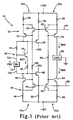
- the symmetrical bipolar bias currents in Gosser's amplifier are provided by a master bias circuit 10 which is illustrated in present FIG. 1, and includes a bandgap reference source 12 which drops a highly stable reference voltage VREF thereacross.
- the source 12 has a positive terminal 12a which is connected through a resistor 14 to the collector of an NPN bipolar transistor 16, and a negative terminal 12b which is connected through a resistor 18 to the emitter of the transistor 16.
- the positive terminal 12a is also connected to the base of the transistor 16.
- a positive current mirror 20 includes a PNP transistor 22 and an NPN transistor 24 which are connected in a Darlington compound transistor configuration, with the emitter of the transistor 24 being connected to the base of the transistor 22 and the collector of the transistor 24 being connected to the emitter of the transistor 22.
- the collector of the transistor 22 is connected to the collector of the transistor 16, whereas the emitter of the transistor 22 is connected through a resistor 26 to a positive voltage supply +VDD.
- the collector of the transistor 22 is also connected to the base of a PNP transistor 28, the collector of which is connected to a negative voltage supply -VEE and the emitter of which is connected to the base of the transistor 24.
- the base of the transistor 24 is further connected to the supply +VDD through a resistor 30 and to the base of an NPN transistor 32.
- the voltage supplies +VDD and -VEE are equal and opposite relative to ground.
- the transistor 32 is connected to a PNP transistor 34 in a Darlington configuration, with the emitter of the transistor 32 being connected to the base of the transistor 34 and the collector of the transistor 32 being connected to the emitter of the transistor 34.
- the emitter of the transistor 34 is connected to the source +VDD through a resistor 36, whereas the collector of the transistor 34 is connected to the positive end of a load 38 which symbolically represents the push-pull amplifier stages of Gosser's device.
- a negative current mirror 40 includes a NPN transistor 42 and a PNP transistor 44 which are connected in a Darlington configuration, with the emitter of the transistor 44 being connected to the base of the transistor 42 and the collector of the transistor 44 being connected to the emitter of the transistor 42.
- the collector of the transistor 42 is connected to the negative terminal 12b of the source 12, whereas the emitter of the transistor 42 is connected through a resistor 46 to the supply -VEE.
- the collector of the transistor 42 is also connected to the base of an NPN transistor 48, the collector of which is connected to the supply +VDD and the emitter of which is connected to the base of the transistor 44.
- the base of the transistor 44 is further connected to the supply -VEE through a resistor 50 and to the base of a PNP transistor 52.
- the transistor 52 is connected to an NPN transistor 54 in a Darlington configuration, with the emitter of the transistor 52 being connected to the base of the transistor 54 and the collector of the transistor 52 being connected to the emitter of the transistor 54.
- the emitter of the transistor 54 is connected to the source -VEE through a resistor 56, whereas the collector of the transistor 54 is connected to the negative end of the load 38.
- a resistor 58 is connected between the emitters of the transistors 24 and 44, whereas a resistor 60 is connected between the emitters of the transistors 32 and 52.
- the resistances of the resistors 58 and 60 are selected to be sufficiently high that the resistors 58 and 60 approximate constant current sources for the transistors 24,44 and 32,52.
- the voltage at the base of the transistor 24 is one forward-biased diode drop Vbe above the voltage at the collector of the transistor 22 due to the base-emitter drop (equal to Vbe) across the transistor 28.
- the voltage at the emitter of the transistor 24 and thereby at the base of the transistor 22 is one diode drop below the voltage at the base of the transistor 24. These two diode drops cancel, such that the voltage at the base of the transistor 22 is equal to the voltage at the collector thereof.
- the Darlington configuration of the transistors 22 and 24 cancels the base current modulation which is present in the transistor 22 in a known manner.
- the transistors 24 and 28 effectively connect the base and collector of the transistor 22 together such that the transistors 22, 24 and 28 in combination are electrically equivalent to a diode.
- the voltage across the resistor 18 is equal to the reference voltage VREF minus the Vbe drop across the base-emitter junction of the transistor 16. This causes a reference current IREF to flow through the resistor 18 and, neglecting the base current of the transistor 16, into the collector and out of the emitter of the transistor 16.
- the bandgap reference source 12, transistor 16 and resistors 14 and 18 constitute a reference current generator 62 which generates the reference current IREF with high precision and stability. Neglecting the base currents of the transistors 28 and 48, the reference current IREF flows from the positive supply +VDD through the resistor 26, transistors 22, 16 and 42 and resistor 46 to the negative supply -VEE.
- the transistors 22, 24 and 28 and resistor 26 constitute an input section 20a of the current mirror 20. Due to the diode connection of the transistor 22, the base (and collector) voltage of the transistor 22 adjusts to a level which accommodates the current IREF flowing therethrough.
- the transistors 32, 34 and 36 constitute an output section 20b of the current mirror 20.
- the base of the transistor 24 is connected to the base of the transistor 32, such that the base voltage of the transistor 34 is equal to the base voltage of the transistor 22.
- the input section 20a of the current mirror 20 acts as a current source which sources the reference current IREF from the supply +VDD into the generator 62, with the current being regulated by the bandgap reference source 12.
- the input section 20a also mirrors the reference current IREF to the output section 20b which sources the reference current (or a corresponding current) from the supply +VDD into the load 38.
- the operation of the current mirror 40 is symmetrical to that of the current mirror 20.
- the input section 40a sinks the current IREF from the generator 62 to the supply -VEE, and mirrors the current IREF to the output section 40b which sinks the current IREF (or a current corresponding to the current sourced by the output section 20b) from the load 38 to the supply -VEE.
- output section 20b and 40b may be replicated to provide one or more additional output sections which are mirrored to the input sections 20a and 40a as indicated by broken lines 64 and 66 respectively.
- the generator 62 and input sections 20a and 40a of the current mirrors 20 and 40 respectively are illustrated in FIG. 2.
- the bases of the transistors 22 and 42 are connected to the collectors thereof, are electrically equivalent to diodes, and are thusly represented in FIG. 2.
- the diode-connected transistors 22 and 42 have very low resistance, and the PSRR is primarily determined by the resistances of the resistors 26, 46, 14 and 18.
- the resistances of these resistors are low, with 26 and 46 being 400 ⁇ and 18 being 300 ⁇ . For this reason, a fluctuation in either of the voltage supplies +VDD and -VEE will modulate the collector-emitter voltage of the transistor 16 and cause a corresponding variation in IREF. This is because due to the very low resistances of the resistors 26, 46 and 18, the collector and emitter voltages of the transistor 16 follow the supply voltages +VDD and -VEE relatively closely, and the PSRR is thereby relatively low.
- Gosser's bias circuit 10 Another problem inherent in Gosser's bias circuit 10 is that the settling during startup is relatively unstable.
- the bandgap reference source 12 is connected in series with the resistor 14 which has a relatively high value (10 K ⁇ ), and is not controlled by any kind of feedback loop.
- the voltage at the upper or lower end of the source 12 is, in the worst case scenario, capable of latching to the supply +VDD or -VEE respectively. This would render the circuit 10 inoperative until the situation was corrected.
- a bandgap reference voltage source has positive and negative terminals which are connected through high impedance constant current sources to positive and negative voltage supplies respectively.
- the effect of variations of the voltage supplies on the voltage source is low due to the high impedances of the currents sources, providing a power supply rejection ratio (PSRR) which is substantially higher than that attainable by the prior art.
- PSRR power supply rejection ratio
- the reference voltage generated by the voltage source is converted into a reference current which flows through two equal series resistors, and also through current mirrors which produce positive and negative output currents corresponding thereto.
- the current sources for the voltage source are also controlled by the current mirrors.
- a servo control amplifier senses the voltage at the junction of the resistors and adjusts the voltage at either the positive or negative terminal of the voltage source to maintain the voltages at the terminals symmetrical with respect to ground, thereby preventing the voltage source from latching to one of the voltage supplies during startup.
- the present invention can alternatively have a unipolar configuration which provides a single bias current.
- one end of the voltage source is tied to ground or other fixed reference, and the servo control function is not required.
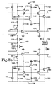
- a symmetrical bipolar (dual polarity) bias current source 100 embodying the present invention is illustrated in FIGs. 3a and 3b.
- the source 100 sources a positive bias current IBIAS into the positive section and sinks the current IBIAS out of the negative section of a load 102, which is typically a symmetrical bipolar push-pull amplifier.
- load 102 which is typically a symmetrical bipolar push-pull amplifier.
- load 102 is typically a symmetrical bipolar push-pull amplifier.
- An exemplary application for the present bias source would be a replacement for the master bias circuit in Gosser's transimpedance amplifier as described above, providing higher PSRR and improved startup operation.
- the present source 100 includes a bandgap reference voltage source 104 having positive and negative terminals 104a and 104b respectively.
- a voltage-to-current converter 106 is responsive to the reference voltage VREF and generates a corresponding reference current IREF which flows through two series connected resistors 108 and 110 which have equal resistances.
- the converter 106 further includes a positive transconductance amplifier 112 and a negative transconductance amplifier 114.
- the amplifier 112 includes a PNP transistor 116 having a base connected to the terminal 104a, a collector connected to ground and an emitter connected to the base of an NPN transistor 118.
- the emitter of the transistor 116 is also connected to a positive voltage supply +VDD through a resistor 117.
- the emitter of the transistor 118 is connected to the upper end of the resistor 108.
- the amplifier 114 includes an NPN transistor 120 having a base connected to the terminal 104b, a collector connected to ground and an emitter connected to the base of a PNP transistor 122.
- the emitter of the transistor 120 is also connected to a negative voltage supply -VEE through a resistor 121.
- the emitter of the transistor 122 is connected to the lower end of the resistor 110.
- the voltage supplies +VDD and -VEE are equal and opposite relative to ground.
- the voltage across the resistors 108 and 110 is equal to VREF. This is because the transistors 116,118 and 120,122 are connected as emitter followers, and the Vbe drops across their base-emitter junctions cancel.
- the bias source 100 further includes a positive current mirror 124 and a negative current mirror 126.
- the mirror 124 includes a PNP transistor 128 and an NPN transistor 130 which are connected in a Darlington compound transistor configuration, with the emitter of the transistor 130 being connected to the base of the transistor 128 and the collector of the transistor 130 being connected to the emitter of the transistor 128.
- the collector of the transistor 128 is connected through a resistor 132 and diode-connected NPN transistor 134 to the collector of the transistor 118, whereas the emitter of the transistor 128 is connected through a resistor 136 to the supply +VDD.
- a capacitor 138 is connected between the collector of the transistor 128 and the supply +VDD.
- the emitter of the transistor 130 is also connected through a resistor 140 to the emitter of a PNP transistor 142, the collector of which is grounded and the base of which is connected to the collector of the transistor 118.
- the transistor 142 is part of and provides a constant bias current for the compound transistor which also includes the transistors 128 and 130.
- the collector of the transistor 128 is also connected to the base of a PNP transistor 144, the collector of which is grounded and the emitter of which is connected to the base of the transistor 130.
- the base of the transistor 130 is further connected to the supply +VDD through a resistor 146 and to the base of an NPN transistor 148.
- the transistor 148 is connected to a PNP transistor 150 in a Darlington configuration, with the emitter of the transistor 148 being connected to the base of the transistor 150 and the collector of the transistor 148 being connected to the emitter of the transistor 150.
- the emitter of the transistor 150 is connected to the source +VDD through a resistor 152, whereas the collector of the transistor 150 is connected to the positive end of the load 102.
- the emitter of the transistor 148 is further connected through a resistor 154 to the emitter of a PNP transistor 156, the collector of which is grounded and the base of which is connected to the collector of the transistor 118.
- the transistor 156 is part of and provides a constant bias current for the compound transistor which also includes the transistors 148 and 150.
- the negative current mirror 126 includes an NPN transistor 158 and a PNP transistor 160 which are connected in a Darlington configuration, with the emitter of the transistor 160 being connected to the base of the transistor 158 and the collector of the transistor 160 being connected to the emitter of the transistor 158.
- the collector of the transistor 158 is connected through a resistor 162 and diode connected PNP transistor 164 to the collector of the transistor 122, whereas the emitter of the transistor 158 is connected through a resistor 166 to the supply -VEE.
- a capacitor 168 is connected between the collector of the transistor 158 and the supply -VEE.
- the emitter of the transistor 160 is also connected through a resistor 170 to the emitter of an NPN transistor 172, the collector of which is grounded and the base of which is connected to the collector of the transistor 122.
- the transistor 172 is part of and provides a constant bias current for the compound transistor which also includes the transistors 158 and 160.
- the collector of the transistor 158 is also connected to the base of an NPN transistor 174, the collector of which is grounded and the emitter of which is connected to the base of the transistor 160.
- the base of the transistor 160 is further connected to the supply -VEE through a resistor 176 and to the base of a PNP transistor 178.
- the transistor 178 is connected to an NPN transistor 180 in a Darlington configuration, with the emitter of the transistor 178 being connected to the base of the transistor 180 and the collector of the transistor 178 being connected to the emitter of the transistor 180.
- the emitter of the transistor 180 is connected to the source -VEE through a resistor 182, whereas the collector of the transistor 180 is connected to the negative end of the load 102.
- the emitter of the transistor 178 is further connected through a resistor 184 to the emitter of an NPN transistor 186, the collector of which is grounded and the base of which is connected to the collector of the transistor 122.
- the transistor 186 is part of and provides a constant bias current for the compound transistor which also includes the transistors 178 and 180.
- the transistors 142, 156, 172 and 186 act as constant current sources for the cascode connected transistors 130, 148, 160 and 178 respectively.
- the diode-connected transistors 134 and 164 provide temperature compensation for the transistors 130 and 160 respectively.
- the voltage at the base of the transistor 130 is one diode drop Vbe above the voltage at the collector of the transistor 128 due to the base-emitter drop across the transistor 144.
- the voltage at the emitter of the transistor 130 and thereby at the base of the transistor 128 is one diode drop Vbe below the voltage at the base of the transistor 130. These two diode drops cancel, such that the voltage at the base of the transistor 128 is equal to the voltage at the collector thereof.
- the Darlington configuration of the transistors 128 and 130 cancels the base current modulation which is present the transistor 128 in a known manner.
- the transistors 130 and 144 effectively connect the base and collector of the transistor 128 together such that the transistor 128 functions electrically as a diode.
- the reference current IREF flows from the positive supply +VDD through the resistor 136, transistor 128, resistor 132 and transistors 134 and 118 into the upper end of the resistor 108.
- the transistors 128, 130, 134, 142 and 144 and resistors 132, 136, 140 and 146 constitute an input section 124a of the current mirror 124. Due to the diode connection of the transistor 128, the base (and collector) voltage of the transistor 128 adjusts to a level which accommodates the current IREF flowing therethrough.
- the transistors 148, 150, 156 and resistors 152 and 154 constitute a first output section 124b of the current mirror 124.
- the base of the transistor 130 is connected to the base of the transistor 148, such that the base voltage of the transistor 150 is equal to the base voltage of the transistor 128.
- the current IBIAS IREF will flow through the transistor 150 into the load 102. If these components are not matched, a current IBIAS will flow through the transistor 150 into the load 102 which corresponds to, but is different from, the reference current IREF.
- the input section 124a of the current mirror 124 mirrors the reference current IREF to the first output section 124b which sources the output current IBIAS which may or may not be equal to IREF from the supply +VDD into the load 102.
- the operation of the current mirror 126 is symmetrical to that of the current mirror 124.
- the input section 126a mirrors the current IREF to a first output section 126b which sinks the current IBIAS from the load 102 to the supply -VEE.
- output section 124b and 126b may be replicated to provide one or more additional output sections which are mirrored to the input sections 124a and 126a as indicated by broken lines 188,189 and 190,191 respectively.
- the current mirrors 124 and 126 further include second output sections 124c and 126c respectively which function as positive and negative current sources for the bandgap reference voltage source 104.
- the output section 124c includes transistors 200, 202 and 204 and resistors 206 and 208 which replicate the transistors 148, 150 and 156 and resistors 152 and 154 of the first output section 124b.
- the second output section 124c further includes a PNP transistor 210 having an emitter connected to the collector of the transistor 200, a collector connected to the positive terminal 104a of the source 104 and a base connected to the collector of the transistor 118.
- the transistor 210 constitutes a cascode stage to increase the impedance between the source +VDD and the terminal 104a.
- the output section 126c includes transistors 212, 214 and 216 and resistors 218 and 220 which replicate the transistors 178, 180 and 186 and resistors 182 and 184 of the first output section 126b respectively.
- the second output section 126c further includes an NPN transistor 222 having an emitter connected to the collector of the transistor 212, a collector connected to the negative terminal 104b of the source 104 and a base connected to the collector of the transistor 122.
- the transistor 222 constitutes a cascode stage to increase the impedance between the source -VEE and the terminal 104b.
- the second output section 124c is mirrored to the input section 124a of the current mirror 124 and sources the reference current IREF (or a current corresponding thereto) from the voltage supply +VDD into the terminal 104a of the source 104.
- the second output section 126c is mirrored to the input section 126a of the current mirror 126 and sinks a current which is equal to the current sourced by the output section 124c from the terminal 104b of the source 104 to the voltage supply -VEE.
- FIG. 4 the transistors 128 and 158 of the input sections 124a and 126a of the current mirrors 124 and 126 respectively are illustrated as diodes, whereas the second output sections 124c and 126c are illustrated as current sources.
- the diode-connected transistors 128 and 158 are electrically equivalent to diodes, and have very low impedance. However, this does not affect the PSRR of the bias circuit 100, since the transistors 128 and 158 are isolated from the voltage source 104 by the generator 106.
- the second output sections 124c and 126c of the current mirrors 124 and 126 respectively which act as current sources for the voltage source 104, do not include diode-connected transistors, and have very high impedance.
- the sections 124c and 126c therefore provide high isolation of the voltage source 104 from the supplies +VDD and -VEE, such that source 104 electrically floats. Due to this isolation, fluctuation of the voltage supplies +VDD and -VEE has negligible effect on the reference current IREF, and the PSRR of the present bias current source 100 is very high compared to the prior art.
- the voltage source 104 is embodied by the National LM113 which has a resistance of approximately 0.3 ⁇ , and the impedances of the second output sections 124c and 126c are each 1 M ⁇
- startup of the bias source 100 requires the generation of the reference current IREF which is fed back via the current mirrors 124 and 126 to provide operating current for the bandgap reference voltage source 104.
- generation of the reference current IREF requires the voltage source 104 to generate the reference voltage VREF, which it cannot do if it does not receive operating current. For this reason, it might not be possible to start up the bias source 100 as described thus far.
- resistors 224 and 226 are connected in parallel with the second output sections 124c and 126c of the current mirrors 124 and 126 respectively.
- the resistors 224 and 226 have resistance values which are as large as possible (to minimize the PSRR) and still enable sufficient trickle current to flow therethrough to provide operating power for the source 104 so that it can generate the reference voltage VREF and the generator 106 can generate the reference current IREF.
- switches 228 and 230 are preferably provided in series with the resistors 224 and 226 respectively to disconnect them from the voltage source 104 after the reference current IREF has been stably generated.
- the switches 228 and 230 may be embodied by switching transistors. The switches 228 and 230 are initially closed, and then opened by a timer or the like (not shown) after sufficient time has elapsed for the bias source 100 to be stably started up.
- the high impedance output sections 124c and 126c of the current mirrors 124 and 126 which act as constant current sources for supplying operating current to the voltage source 104 electrically isolate the source 104 from the supplies +VDD and -VEE respectively. Since the source 104 electrically floats, it is possible for the upper or lower end of the source 104 to float toward the supply +VDD or -VEE and latch at the respective supply voltage, rendering the bias current source 100 inoperative until the situation is corrected.
- the source 100 further includes a servo control amplifier 232 for clamping a junction 234 between the resistors 108 and 110 to ground and thereby maintaining the voltages at the terminals 104a and 104b of the source 104 equal and opposite relative to ground.
- the amplifier 232 is illustrated symbolically in FIG. 4, and the detailed circuit configuration thereof is illustrated in FIG. 3a.
- the amplifier 232 is essentially a differential-to-single-ended converter, and includes NPN transistors 236 and 238 having emitters which are interconnected by resistors 240 and 242 respectively.
- the junction of the resistors 240 and 242 is connected through a resistor 244 to the source -VEE.
- the base of the transistor 236 is connected to ground through a resistor 246, whereas the base of the transistor 238 is connected to the junction 234.
- the base of the transistor 236 constitutes a non-inverting input of the amplifier 232, whereas the base of the transistor 238 constitutes an inverting input thereof.
- the collectors of the transistors 236 and 238 are connected to the collectors of PNP transistors 248 and 250, the emitters of which are interconnected by resistors 252 and 254 respectively.
- a capacitor 256 is connected across the collectors of the transistors 248 and 250.
- the base and collector of the transistor 248 are interconnected in a diode configuration.
- the transistors 248 and 250 constitute a current mirror, with the current through the transistor 248 being mirrored to the transistor 250.
- the junction of the resistors 252 and 254 is connected through a level shifting circuit 258 to the supply +VDD.
- the circuit 258 includes an NPN transistor 260 having an emitter connected to the junction of the resistors 252 and 254 and a collector connected to the supply +VDD.
- a voltage divider for biasing the base of the transistor 260 includes a resistor 262 connected between the base of the transistor 260 and the source +VDD, and a resistor 264 connected between the base of the transistor 260 and ground.
- a capacitor 266 is connected in parallel with the resistor 264.
- the collector of the transistor 238, which constitutes the output of the amplifier 232, can be connected to the terminal 104a of the voltage source 104 as illustrated in solid line, or to the terminal 104b thereof as illustrated in broken line. The operation of the amplifier 232 will produce the same result in either case.
- the amplifier 232 compares the voltage at the junction of the resistors 108 and 110 which appears at its inverting input to ground which appears at its non-inverting input.
- the voltage across the resistors 108 and 110 in series will not vary from VREF.
- the voltage source 104 electrically floats due to the high impedance of its current sources, the voltages at the ends of the resistors 108 and 110 and corresponding the voltages at the terminals 104a and 104b can drift together relative to ground in a common mode manner.
- the voltage at the junction 234 is equal to the voltage at the upper end of the resistor 108 and at the lower end of the resistor 110 level shifted up and down by VREF/2 respectively. If these voltages are equal and opposite relative to ground, the voltage at the junction 234 will be zero and the output of the amplifier 232 will be zero. Assuming that the voltages drift upwardly (go more positive), the voltage at the junction 234 and at the inverting input (base of the transistor 238) of the amplifier 232 will increase by the same amount. The transistor 238 will conduct more current than the transistor 240, and the voltage at the output (collector of the transistor 238) of the amplifier 232 will decrease (go negative).
- the negative output voltage of the amplifier 232 will cause the voltage at the terminal 104a or 104b to which it is connected to decrease.
- the voltages at the terminals 104a and 104b move together due to the fixed voltage drop VREF across the voltage source 104. This operation causes the voltages at the terminals 104a and 104b to move downwardly (more negative) until they are equal and opposite relative to ground and the voltage at the junction 234 is equal to ground.
- the operation of the amplifier 232 is opposite to that described above when the voltages at the terminals 104a 104b and at the junction 234 drift downwardly (go more negative).
- a unipolar bias source generally consists of the upper half of the bias current source 100 for producing a positive bias current, or the lower half of the source 100 for producing a negative bias current.
- one end of the bandgap reference voltage source is tied to ground or other fixed reference, and the servo control function is not required.
- FIG. 5 illustrates a unipolar bias current source 300 embodying the present invention which includes a bandgap reference voltage source 302 which produces a voltage drop VREF thereacross.
- a voltage-to-current converter 304 in the form of a transconductance amplifier is responsive to the reference voltage VREF and causes a reference current IREF corresponding thereto to flow through a resistor 306.
- the reference current IREF flows through an input section 308a of a current mirror 308, and is mirrored to a first output section 308b which sources a corresponding current IBIAS into a load 310 and to a second output section 308c which sources an operating current for the source 302.
- the source 302 has a negative terminal 302b which is connected to ground and a positive terminal 302a which is connected to the base of a PNP transistor 312 of the converter 304.
- the collector of the transistor 312 is connected to ground, whereas the emitter of the transistor 312 is connected to a voltage supply +VDD through a resistor 314.
- the emitter of the transistor 312 is also connected to the base of a transistor 316, the emitter of which is connected to ground through the resistor 306.
- the input section 308a of the current mirror 308 includes a diode-connected PNP transistor 318 having a collector connected to the collector of the transistor 316 and an emitter connected to the supply +VDD through a resistor 320.
- the first output 308b section of the current mirror 308 includes a PNP transistor 322 having a base connected to the base of the transistor 318, an emitter connected through a resistor 324 to the supply +VDD and a collector connected to the load 310.
- the second output section 308c of the current mirror 308 includes a PNP transistor 326 having a base connected to the base of the transistor 318, an emitter connected to the supply +VDD through a resistor 328 and a collector connected to the terminal 302a of the source 302.
- the operation of the bias current source 300 is essentially similar to that of the upper half of the bias current source 100 illustrated in FIGs. 3a and 3b.
- the current mirror 308 is illustrated in its most basic form in FIG. 5.
- the scope of the invention includes replacing the transistors 318, 322 and 326 with Darlington type compound transistors as in the current mirrors of the source 100 to provide improved performance. It is also within the scope of the invention to replace the current mirrors in the source 100 with simple current mirrors as illustrated in FIG. 5, Wilson current mirrors, or any other suitable type of current mirrors.
- CMOS complementary-metal-oxide-semiconductor
Landscapes
- Engineering & Computer Science (AREA)
- Power Engineering (AREA)
- Amplifiers (AREA)
- Control Of Electrical Variables (AREA)
Applications Claiming Priority (2)
| Application Number | Priority Date | Filing Date | Title |
|---|---|---|---|
| US976760 | 1992-11-16 | ||
| US07/976,760 US5315231A (en) | 1992-11-16 | 1992-11-16 | Symmetrical bipolar bias current source with high power supply rejection ratio (PSRR) |
Publications (2)
| Publication Number | Publication Date |
|---|---|
| EP0598578A2 true EP0598578A2 (de) | 1994-05-25 |
| EP0598578A3 EP0598578A3 (de) | 1994-10-05 |
Family
ID=25524433
Family Applications (1)
| Application Number | Title | Priority Date | Filing Date |
|---|---|---|---|
| EP9393309101A Withdrawn EP0598578A3 (de) | 1992-11-16 | 1993-11-15 | Symmetrische Vorspannungs-Stromquelle mit Bipolartransistoren mit grosser Störunterdrückung der Stromversorgung. |
Country Status (3)
| Country | Link |
|---|---|
| US (1) | US5315231A (de) |
| EP (1) | EP0598578A3 (de) |
| JP (1) | JP3479108B2 (de) |
Cited By (3)
| Publication number | Priority date | Publication date | Assignee | Title |
|---|---|---|---|---|
| EP1229420A1 (de) * | 2001-01-31 | 2002-08-07 | STMicroelectronics S.r.l. | Bandabstands-Referenzspannung mit niedriger Versorgungsspannung |
| EP1313212A1 (de) * | 2001-11-19 | 2003-05-21 | Dialog Semiconductor GmbH | Störunterdrückungsoptimierung der Stromversorgung während des Prüfens |
| US6905506B2 (en) | 2001-03-28 | 2005-06-14 | Vascular Control Systems, Inc. | Multi-axial uterine artery identification, characterization, and occlusion pivoting devices and methods |
Families Citing this family (12)
| Publication number | Priority date | Publication date | Assignee | Title |
|---|---|---|---|---|
| FR2722636B1 (fr) * | 1994-07-15 | 1996-09-20 | Le Tourneur Gregoire | Dispositif de prise de son par microphone electret |
| DE69629549T2 (de) * | 1995-11-21 | 2004-06-17 | Koninklijke Philips Electronics N.V. | Anordnung mit einem magnetschreibkopf und schreibverstärker mit kapazitiver, vorwärtsgekoppelter kompensation |
| US5726600A (en) * | 1996-01-17 | 1998-03-10 | Hughes Aircraft Company | NPN bipolar circuit topology for a tunable transconductance cell and positive current source |
| US5726563A (en) * | 1996-11-12 | 1998-03-10 | Motorola, Inc. | Supply tracking temperature independent reference voltage generator |
| US5867056A (en) * | 1997-11-14 | 1999-02-02 | Fluke Corporation | Voltage reference support circuit |
| FR2772155B1 (fr) * | 1997-12-10 | 2000-02-11 | Matra Mhs | Dispositif de generation d'une tension continue de reference |
| US6016050A (en) * | 1998-07-07 | 2000-01-18 | Analog Devices, Inc. | Start-up and bias circuit |
| US6667614B1 (en) * | 2000-02-16 | 2003-12-23 | Seagate Technology Llc | Transfer curve tester for testing magnetic recording heads |
| US6509727B2 (en) * | 2000-11-24 | 2003-01-21 | Texas Instruments Incorporated | Linear regulator enhancement technique |
| US7728574B2 (en) * | 2006-02-17 | 2010-06-01 | Micron Technology, Inc. | Reference circuit with start-up control, generator, device, system and method including same |
| US9072044B2 (en) * | 2012-11-30 | 2015-06-30 | Intel Mobile Communications GmbH | Push-pull amplifier with quiescent current adjuster |
| US20190356877A1 (en) * | 2018-05-17 | 2019-11-21 | Sony Semiconductor Solutions Corporation | Image sensor with s/h-to-adc voltage range matching |
Family Cites Families (4)
| Publication number | Priority date | Publication date | Assignee | Title |
|---|---|---|---|---|
| JPS6054508A (ja) * | 1983-09-06 | 1985-03-29 | Pioneer Electronic Corp | エミッタホロワ型シングルエンデットプッシュプル回路 |
| US4933644A (en) * | 1988-12-23 | 1990-06-12 | Texas Instruments, Incorporated | Common-mode feedback bias generator for operational amplifiers |
| US4970470A (en) * | 1989-10-10 | 1990-11-13 | Analog Devices, Incorporated | DC-coupled transimpedance amplifier |
| JP3058935B2 (ja) * | 1991-04-26 | 2000-07-04 | 株式会社東芝 | 基準電流発生回路 |
-
1992
- 1992-11-16 US US07/976,760 patent/US5315231A/en not_active Expired - Lifetime
-
1993
- 1993-11-15 EP EP9393309101A patent/EP0598578A3/de not_active Withdrawn
- 1993-11-16 JP JP28702693A patent/JP3479108B2/ja not_active Expired - Fee Related
Cited By (5)
| Publication number | Priority date | Publication date | Assignee | Title |
|---|---|---|---|---|
| EP1229420A1 (de) * | 2001-01-31 | 2002-08-07 | STMicroelectronics S.r.l. | Bandabstands-Referenzspannung mit niedriger Versorgungsspannung |
| US6680643B2 (en) | 2001-01-31 | 2004-01-20 | Stmicroelectronics S.R.L. | Bandgap type reference voltage source with low supply voltage |
| US6905506B2 (en) | 2001-03-28 | 2005-06-14 | Vascular Control Systems, Inc. | Multi-axial uterine artery identification, characterization, and occlusion pivoting devices and methods |
| EP1313212A1 (de) * | 2001-11-19 | 2003-05-21 | Dialog Semiconductor GmbH | Störunterdrückungsoptimierung der Stromversorgung während des Prüfens |
| US6603293B2 (en) | 2001-11-19 | 2003-08-05 | Dialog Semiconductor Gmbh | Power supply rejection ratio optimization during test |
Also Published As
| Publication number | Publication date |
|---|---|
| US5315231A (en) | 1994-05-24 |
| EP0598578A3 (de) | 1994-10-05 |
| JP3479108B2 (ja) | 2003-12-15 |
| JPH077341A (ja) | 1995-01-10 |
Similar Documents
| Publication | Publication Date | Title |
|---|---|---|
| US5315231A (en) | Symmetrical bipolar bias current source with high power supply rejection ratio (PSRR) | |
| US4626770A (en) | NPN band gap voltage reference | |
| US4349778A (en) | Band-gap voltage reference having an improved current mirror circuit | |
| US4435678A (en) | Low voltage precision current source | |
| US4446419A (en) | Current stabilizing arrangement | |
| US5319303A (en) | Current source circuit | |
| EP0463857B1 (de) | Emittergeerdete Verstärkerschaltung mit Vorspannungsschaltung | |
| JP2005011067A (ja) | 定電圧発生器 | |
| US4734598A (en) | Controllable integrator | |
| US4567426A (en) | Current stabilizer with starting circuit | |
| US4334198A (en) | Biasing of transistor amplifier cascades | |
| JPH11514193A (ja) | 温度補償増幅器 | |
| US4441070A (en) | Voltage regulator circuit with supply voltage ripple rejection to transient spikes | |
| US4219781A (en) | Transistor amplifier circuit | |
| JPH0259912A (ja) | 差動電圧源 | |
| EP0596653A1 (de) | Niederspannungs-Referenzstromgeneratorschaltung | |
| US7113041B2 (en) | Operational amplifier | |
| JPH07104372B2 (ja) | 電圧比較回路 | |
| US4413226A (en) | Voltage regulator circuit | |
| US4667145A (en) | Voltage regulator circuit | |
| US4329598A (en) | Bias generator | |
| EP0288697B1 (de) | Massstabgerechte Spannungspegelumsetzungsschaltung | |
| US4851759A (en) | Unity-gain current-limiting circuit | |
| US6683444B2 (en) | Performance reference voltage generator | |
| US4524330A (en) | Bipolar circuit for amplifying differential signal |
Legal Events
| Date | Code | Title | Description |
|---|---|---|---|
| PUAI | Public reference made under article 153(3) epc to a published international application that has entered the european phase |
Free format text: ORIGINAL CODE: 0009012 |
|
| AK | Designated contracting states |
Kind code of ref document: A2 Designated state(s): DE FR GB |
|
| PUAL | Search report despatched |
Free format text: ORIGINAL CODE: 0009013 |
|
| AK | Designated contracting states |
Kind code of ref document: A3 Designated state(s): DE FR GB |
|
| 17P | Request for examination filed |
Effective date: 19950309 |
|
| 17Q | First examination report despatched |
Effective date: 19961204 |
|
| 18D | Application deemed to be withdrawn |
Effective date: 19980130 |