EP0598849B1 - Circuits et procedes d'alimentation a decoupage a faible puissance - Google Patents
Circuits et procedes d'alimentation a decoupage a faible puissance Download PDFInfo
- Publication number
- EP0598849B1 EP0598849B1 EP92919283A EP92919283A EP0598849B1 EP 0598849 B1 EP0598849 B1 EP 0598849B1 EP 92919283 A EP92919283 A EP 92919283A EP 92919283 A EP92919283 A EP 92919283A EP 0598849 B1 EP0598849 B1 EP 0598849B1
- Authority
- EP
- European Patent Office
- Prior art keywords
- voltage
- circuit
- primary inductor
- flyback
- control
- Prior art date
- Legal status (The legal status is an assumption and is not a legal conclusion. Google has not performed a legal analysis and makes no representation as to the accuracy of the status listed.)
- Expired - Lifetime
Links
Images

Classifications
-
- G—PHYSICS
- G05—CONTROLLING; REGULATING
- G05F—SYSTEMS FOR REGULATING ELECTRIC OR MAGNETIC VARIABLES
- G05F1/00—Automatic systems in which deviations of an electric quantity from one or more predetermined values are detected at the output of the system and fed back to a device within the system to restore the detected quantity to its predetermined value or values, i.e. retroactive systems
- G05F1/10—Regulating voltage or current
- G05F1/46—Regulating voltage or current wherein the variable actually regulated by the final control device is DC
- G05F1/56—Regulating voltage or current wherein the variable actually regulated by the final control device is DC using semiconductor devices in series with the load as final control devices
- G05F1/563—Regulating voltage or current wherein the variable actually regulated by the final control device is DC using semiconductor devices in series with the load as final control devices including two stages of regulation at least one of which is output level responsive, e.g. coarse and fine regulation
-
- H—ELECTRICITY
- H02—GENERATION; CONVERSION OR DISTRIBUTION OF ELECTRIC POWER
- H02M—APPARATUS FOR CONVERSION BETWEEN AC AND AC, BETWEEN AC AND DC, OR BETWEEN DC AND DC, AND FOR USE WITH MAINS OR SIMILAR POWER SUPPLY SYSTEMS; CONVERSION OF DC OR AC INPUT POWER INTO SURGE OUTPUT POWER; CONTROL OR REGULATION THEREOF
- H02M3/00—Conversion of DC power input into DC power output
- H02M3/22—Conversion of DC power input into DC power output with intermediate conversion into AC
- H02M3/24—Conversion of DC power input into DC power output with intermediate conversion into AC by static converters
- H02M3/28—Conversion of DC power input into DC power output with intermediate conversion into AC by static converters using discharge tubes with control electrode or semiconductor devices with control electrode to produce the intermediate AC
- H02M3/325—Conversion of DC power input into DC power output with intermediate conversion into AC by static converters using discharge tubes with control electrode or semiconductor devices with control electrode to produce the intermediate AC using devices of a triode or a transistor type requiring continuous application of a control signal
- H02M3/335—Conversion of DC power input into DC power output with intermediate conversion into AC by static converters using discharge tubes with control electrode or semiconductor devices with control electrode to produce the intermediate AC using devices of a triode or a transistor type requiring continuous application of a control signal using semiconductor devices only
- H02M3/33507—Conversion of DC power input into DC power output with intermediate conversion into AC by static converters using discharge tubes with control electrode or semiconductor devices with control electrode to produce the intermediate AC using devices of a triode or a transistor type requiring continuous application of a control signal using semiconductor devices only with automatic control of the output voltage or current, e.g. flyback converters
Definitions
- This invention relates generally to power supplies for electronic circuitry, and more particularly, to flyback power supply circuits having regulated voltage outputs.
- the power supply will be described in the context of a power supply for a process control transducer, by way of illustration.
- electrical and electronic process control loops were a natural development from prior electromechanical control systems.
- the general problem of electronic process control is to convert a physical variable to an electrical signal, and to subsequently transmit that signal to a recorder and/or other control equipment which may be located some distance away from the physical variable.
- Early types of process control loops to accomplish this goal were "four-wire" systems, and were configured such that operating power was supplied through two of the four wires and a process signal was transmitted through the other two wires.
- the four-wire system requires the use of amplifiers or other signal conditioning equipment at the point of measurement in order to supply an accurate signal representative of the physical variable since the process signal is generally very low. See, e.g. , U.S. Patent No. 3,680,384, of Grindheim.
- Prior four-wire transmitter systems thus required separate power supply lines, and voltage power supplies.
- the four-wire transmitter was developed, it became apparent that the advantages of using the same two wires for power supply and information transmission would greatly improve the process control art.
- the "two-wire" transmitter was then developed and operates today in a control loop in conjunction with an external power supply, a pair of wires from the supply, and a transmitter connected serially between the wires.
- the term "two-wire” is construed broadly to mean two conductors.
- the term “two-wire” includes actual wires, twisted pairs, coaxial cables, and other pairs of conductors.
- the transmitter energizes a sensor element and receives informational signals from the sensor element.
- the information is transmitted on the pair of wires by varying the current in the current loop.
- the transmitter acts as a variable current sink, and the amount of current which it sinks is representative of the information from the sensor.
- Such prior two-wire transmitter loops have generally been analog in nature, and the industry standard which has developed for two-wire transmitters is a 4 to 20 milliamp loop, with a variable loop supply voltage having a maximum output of 42 volts DC. With such a low voltage supply, two-wire transmitter loops are particularly suited for use in hazardous environments. See , e.g., U.S. Patent No. 4,242,665, of Mate.
- More advanced prior two-wire transmitter control loops exhibit high-level data communication between two-wire transmitters and various receiving elements, for example controllers and communication devices.
- the concept of digital communication in 4 to 20 milliamp control systems is known for use in the more complicated 4 to 20 milliamp loops having both digital and analog components.
- Transmitters suitable for such purposes are usually called “smart" transmitters because they are more accurate and have operating parameters which may be remotely controlled.
- flyback regulator control circuits In flyback regulator control circuits, generally two methods have been used to sense the inductor current.
- the flyback inductor saturation current may be sensed, or a shunt resistor can be placed in series with the flyback inductor to directly sense the state of the flyback inductor current.
- both of these current sensing techniques introduce a large amount of power loss to the power supply, and therefore are unacceptable for use in low power 40 milliwatt systems.
- Prior power supplies using these methods of sensing the inductor current simply do not fulfill a long-felt need in the art for low power loss switching power supplies for electronic circuitry.
- Two-wire transmitters are often remotely located.
- the length of the wires connecting components in the loop can exceed 5000 feet (approximately 1500 m), and the longer wires have higher resistance. This resistance reduces the voltage to the transmitter.
- Other devices such as indicators, recorders and barriers are usually added to the loop, further increasing the loop resistance. Large amounts of loop resistance cause a wide variation in the input voltage. Changes of load current can vary widely also as different digital systems are accessed. The combination of high line variation and high load variation place a difficult burden on the traditional methods of switching power supply control circuits which have the further requirement of low startup current.
- the invention relates to a flyback power supply circuit, comprising linear regulator means for receiving an unregulated voltage for regulating input power to the power supply and producing a linearly regulated voltage; a flyback voltage generator comprising a flyback transformer having a primary inductor and a secondary inductor coupled to each other, the primary inductor being coupled to the output of the linear regulator means; a source of DC input voltage, and pulser means connected to the source of DC input voltage for passing current pulses through the primary inductor; circuit means connected to the secondary inductor for developing a regulated direct output voltage in response to flyback pulses generated in the secondary inductor by the terminations of the primary inductor current pulses; timer means for controlling the times of initiation and termination of the primary inductor pulses in response to control signals supplied thereto, to regulate the direct output voltage; and monitor means coupled between the linear regulator means and the flyback voltage generator for monitoring the output voltage and causing the flyback voltage generator to produce a power pulse having a width dependent on the unregulated input voltage, the monitor
- the timer means comprises a first R-C circuit supplied with the input voltage for controlling the durations of the primary inductor current pulses as a function of the input voltage; a second circuit responsive to the output voltage for providing continuous control of the repetition frequency of the primary inductor current pulses as a function of the output voltage; an override circuit connected to the primary inductor for terminating any of the primary inductor current pulses, the intensity of which reaches a predetermined level; the first R-C circuit having a charging time constant analogous to that of the primary inductor, the timer means being responsive to the input voltage to decrease the durations of said primary inductor pulses when said supplied voltage increases and to increase their durations when the supplied voltage decreases; the second circuit being responsive to variations in the direct output voltage to increase the pulse repetition frequency continuously when the direct output voltage tends to decrease and to decrease the pulse repetition frequency continuously when the direct output voltage tends to increase; the override circuit comprising means for sensing the intensities of
- the preferred embodiment constitutes a highly efficient power supply with very little power loss due to regulation or control of the circuits.
- three modes of control are preferably used. These are an indirect sense feedforward control, a feedback control, and an override control.
- the circuit provides a highly efficient regulated power source for low power electronic instrumentation, and greatly increases the efficiency of two-wire transmitters and process control loops which utilize these circuits.
- a switching power supply circuit as described herein can have a performance efficiency of about 90%. Such results have not heretofore been achieved in the art and solve a long-felt need in the art for low power loss, high efficiency switching power supplies for use in low power electronic circuits and systems.
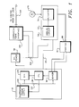
- FIG. 1 is a schematic block diagram of a two-wire transmitter process control loop utilizing a switching power supply provided in accordance with the present invention.
- a two-wire transmitter 10 provides an output 4 to 20 milliamp analog signal 20 to the control loop.
- Transmitter 10 is preferably a two-wire transmitter which has a sensing element 30 interfaced with a process 40 which the loop monitors and controls.
- the process 40 may be any type of industrial process such as fluid flow, level, pressure, temperature, or any other type of process having a process variable which it is desired to monitor.
- the two-wire transmitter 10 may also provide control functions to the loop and the 4 to 20 milliamp analog signal 20 may also therefore be a 4 to 20 milliamp control signal adapted to interface with a final control element 50.
- the final control element 50 in preferred embodiments comprises an analog circuit 60 directly interfaced with the 4 to 20 milliamp analog signal 20.
- An analog circuit 60 is interfaced with an actuator 70 which is further interfaced at 80 with the process 40.
- Analog circuit 60 receives and interprets the 4 to 20 milliamp analog control signal 20 and busses this signal to the actuator 70.
- the actuator 70 may actuate a valve to control the process variable when the process is a fluid flow process, for example.
- the actuator and control element 50 interfaced at 80 with the process 40 provides control of the process variable in accordance with a particular control protocol that is designed for the industrial application in which the control system is placed.
- the control system is preferably powered by a DC power supply 90 having a fixed output of up to 42 volts DC.
- the entire DC power to run the loop is provided by DC power supply 90, and so the entire 4 to 20 milliamp analog range appears on the control loop by virtue of the DC power supply 90.
- DC power supply 90 is directly interfaced to the transmitter 10 to provide unregulated power to the transmitter.
- a switching power supply 100 regulates the power received by DC power supply 90 and outputs the regulated power onto a power bus 110 to supply the various circuit components in the transmitter 10.
- the circuit components in the transmitter 10 such as a digital-to-analog (D/A) converter 120, a system CPU 130, and the sensor 30, as well as other necessary circuitry in the transmitter 10 and components in the loop, have regulated power supplied to them by the switching power supply 100.
- the switching power supply 100 is preferably a 40 milliwatt power supply having an efficiency of between about 30% and 90%.
- a digital communications interface 140 is interfaced with the control loop at 150 and provides the ability for the control loop to have a digital, bidirectional communications protocol superimposed on the 4 to 20 milliamp analog signal. Communications interface 140 also busses information at 160 to a control room or user in digital form. This digital information is usually related to loop parameter values and the process variable especially when the transmitter 10 operates in a controller mode to control the process 40.
- An AC power supply 170 is optionally provided to supply additional power to the final control element 50 especially when the actuator 70 is interfaced with an electromechanical valve requiring a strong electromagnetic force to actuate the valve.
- AC power 170 in preferred embodiments provides enough power to actuate a heavy duty control valve in pressure and flow applications.
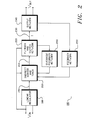
- Linear regulator means 180 provides initial regulation of V in (a 10 to 42 volt DC level) and initially conditions V in to a linearly regulated voltage 190 which is further input to the switching power supply.
- the linear regulator means 180 produces a linearly regulated voltage V + which is used by the rest of the circuit to produce V out .
- the unregulated input voltage V in is input to a monitoring means 200 which is preferably adapted to monitor the output voltage V out and to control V out with internal timing, direct, and indirect sensing elements which comprise the monitoring means 200.
- the output 210 from the monitoring means 200 is input to standard flyback regulator and switch means 220 which is adapted to provide an output current 230 to an output network 240.
- An override feedback block 280 preferably directly senses abnormal currents in the flyback means 220 and resets monitoring means 200.
- the output network 240 conditions the current and converts it to the output voltage V out which is then usable by the electronic circuitry in the two-wire transmitter and powers the instrumentation in the control loop.
- a feedback network 250 is provided interfaced with the output network 240 for feeding back part of the output voltage V out to the monitoring block 200 having the indirect sensing and timing elements therein. In this fashion, feedback network 250 controls the pulse repetition rate of the output.
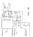
- FIG. 3 is a detailed circuit diagram of a preferred embodiment of a switching power supply.
- Q1, Q2, Q3, R1 through R5 and the zener diode VR1 comprise the linear regulator 180.
- the linear regulator 180 allows a wide range of input voltages to be used, anywhere from 10 to 42 volts DC.
- Q2 and Q3 make up a difference amplifier circuit wherein the difference between the reference voltage and the feedback output is amplified and drives the field effect transistor (FET) Q1 providing series regulation of V + .
- FET field effect transistor
- the monitoring means 200 having an indirect sensing means and timing element comprises the components R6, R7, C2, C4, U2 (which in preferred embodiments is an ICM7555 timing chip hereinafter referred to as a "555 timer") and CR1.
- the output from the timing chip is input at 210 to the flyback regulator 220 which further comprises Q4, an insulated gate FET or MOSFET, and an inductor coil T1 operating in the flyback mode.
- the current 230 output from the flyback regulator circuit 220 is input to the output network 240 which comprises capacitors C6 and C7 and diodes CR2 and CR3.
- An isolated output 260 and a 5-volt output 270 are output from the output circuit 240.
- a feedback signal from the 5-volt output 270 is input to feedback network 250 which is further interfaced to the monitoring circuit 200 to provide control of the pulse repetition rate of the output circuit from flyback regulator circuit 220.
- the linear regulator circuit 180 supplies a voltage V + to the 555 timer at pin eight in the monitoring circuit 200.
- the 555 timer switches Q4 in the flyback regulator block 220 such that T1 is operated in the flyback mode charging C6 and C7 in the output network 240.
- the current in the coil T1 is not directly sensed but, instead, Q4 is switched off when the voltage on C2 is two thirds V + . This eliminates the need for sensing the inductor saturation current which would otherwise dissipate an unacceptable amount of power in the circuit.
- the values of R6 and C2 in the monitoring circuit 200 are chosen such that the voltage on C2 reaches two thirds V + at the same time the current in T1 reaches the desired threshold current.
- the series network comprising R6 and C2 provides an indirect sensing element for the monitoring circuit 200 to, in effect, "sense" the current through T1 in the flyback regulator circuit 220. Since the voltage on C2 reaches two thirds V + at the same time the current in T1 reaches the desired threshold, and both of these events are proportional to V in , they occur simultaneously regardless of the value of V in .
- capacitor C2 When Q4 in the flyback regulator block 220 is switched off, capacitor C2 is preferably discharged to 0 volts, and inductor T1 to 0 current.
- the output voltage 270 is then sensed through R10 and R11 in feedback network 250 and fed back to a difference amplifier comprising Q6 and Q7 in the feedback circuit 250 whose output triggers the 555 timer.
- the current through Q6 in feedback circuit 250 and the current through the capacitor C4 in monitoring block 200 set a repetition rate of the pulses to control the output voltage 270.
- the 555 timer output shown at pin three, charges capacitor C4 through diode CR1.
- diode CR1 is reversed biased.
- transistor Q6 in feedback network 250 discharges capacitor C4 in monitoring circuit 200 and triggers a new output pulse when the voltage value on capacitor C4 reaches one third V in .
- transistor Q5 and resistor R8 preferably act as an override control and limit the current in transistor Q4 to a safe level.
- the value of the sensing resistor R8 in override feedback block 280 is preferably small so that during normal operation it does not decrease the efficiency of circuit 100.
- the circuit 100 shown in Figure 3 provides the advantage of indirectly sensing the current through the inductor T1 with a separate RC network comprising resistor R6 and C2 such that the RC time constant in parallel with T1 emulates the inductor T1's time constant.
- the current across T1 preferably ramps up in the same time as the voltage across C2 so that the RC time constant maintains the inductor T1's time constant to the same value.
- This provides a low power indirect sensing element and eliminates the need for a high value shunt resistor in series with the inductor, or direct sensing of the inductor saturation current for regulated control.
- the general purpose 555 timer U2 provides feedback control through the switching power supply 100.
- a "threshold” feedback pin 6 is provided for varying the pulse width with input voltage change to produce the output voltage 270.
- the "trigger" feedback path, pin two, of the 555 timer U2 controls the pulse frequency and senses the output voltage change through the feedback network 250.
- a "reset” feedback, pin 4 provides soft start-up with resistor R8 coupled to the primary of transformer T1 to provide an over-current sensor, and to protect transistor Q4 during start-up.
- the circuit 100 of Figure 3 provides a regulated 40 milliwatt power budget to electronic instrumentation in a two-wire control loop.
- This circuit has an approximately 90% power regulation efficiency which has not heretofore been achieved in the art, thereby allowing efficient and constant 40 milliwatt power to be provided continuously to the loop. Such results have not heretofore been achieved in the art and provide great advantages over prior circuits and networks of a power regulation.
Landscapes
- Engineering & Computer Science (AREA)
- Power Engineering (AREA)
- Physics & Mathematics (AREA)
- Electromagnetism (AREA)
- General Physics & Mathematics (AREA)
- Radar, Positioning & Navigation (AREA)
- Automation & Control Theory (AREA)
- Dc-Dc Converters (AREA)
- Direct Current Feeding And Distribution (AREA)
Claims (2)
- Circuit d'alimentation en énergie du type indirect, comportant :caractérisé en ce que le moyen à rythmeur (U2) comporte un premier circuit R-C (R6, C2) alimenté par la tension d'entrée (Vin) pour régler les durées des impulsions de courant de l'inductance primaire en fonction de la tension d'entrée ;un moyen à régulateur linéaire (180) destiné à recevoir une tension non régulée (Vin) pour réguler de l'énergie d'entrée fournie à l'alimentation en énergie et produire une tension régulée linéairement ;un générateur indirect (220) de tension comportant un transformateur indirect (T1) ayant une inductance primaire et une inductance secondaire couplées entre elles, l'inductance primaire étant couplée à la sortie du moyen à régulateur linéaire (180) ;une source de tension d'entrée continue, un moyen (Q4) de production d'impulsions connecté à la source de tension d'entrée continue pour faire passer des impulsions de courant dans l'inductance primaire ;un moyen à circuit (240) connecté à l'inductance secondaire pour développer une tension continue régulée de sortie en réponse à des impulsions de retour générées dans l'inductance secondaire par les cessations des impulsions de courant de l'inductance primaire ;un moyen à rythmeur (U2) destiné à commander les temps d'amorçage et de cessation des impulsions de l'inductance primaire en réponse à des signaux de commande qui lui sont appliqués, pour réguler la tension continue de sortie ; etun moyen de contrôle (200) monté entre le moyen à régulateur linéaire (180) et le générateur indirect (220) de tension pour contrôler la tension de sortie et amener le générateur indirect de tension à produire une impulsion d'énergie ayant une largeur dépendant de la tension d'entrée non régulée (Vin), le moyen de contrôle (200) comprenant le moyen à rythmeur (U2) ;un second circuit (C4, 250) qui, en réponse à la tension de sortie, produit un réglage continu de la fréquence de répétition des impulsions de courant de l'inductance primaire en fonction de la tension de sortie ;un circuit à priorité (280) connecté à l'inductance primaire pour faire cesser n'importe laquelle des impulsions de courant de l'inductance primaire dont l'intensité atteint un niveau prédéterminé ;le premier circuit R-C (R6, C2) ayant une constante de temps de charge analogue à celle de l'inductance primaire, le moyen à rythmeur (U2) réagissant à la tension d'entrée (Vin) en diminuant les durées desdites impulsions de l'inductance primaire lorsque ladite tension d'alimentation (Vin) augmente, et en augmentant leurs durées lorsque la tension d'alimentation (Vin) diminue ;le second circuit (C4, 250) réagissant à des variations de la tension continue de sortie en augmentant en continu la fréquence de répétition des impulsions lorsque la tension continue de sortie tend à diminuer, et en diminuant en continu la fréquence de répétition des impulsions lorsque la tension continue de sortie tend à augmenter ;le circuit (280) à priorité comportant un moyen pour capter les intensités des impulsions de courant passant dans l'inductance primaire afin de produire un signal de commande, et un moyen destiné à appliquer le signal de commande pour faire cesser n'importe laquelle des impulsions lorsque son intensité atteint un niveau prédéterminé.
- Alimentation en énergie selon la revendication 1, dans laquelle le circuit à priorité (280) comporte un moyen résistif (R8) en série avec l'inductance primaire pour développer une tension de commande à priorité proportionnelle aux intensités des impulsions de courant de l'inductance primaire, et un moyen destiné à appliquer la tension de commande à priorité pour faire cesser toute impulsion de courant primaire dont l'intensité s'élève jusqu'au niveau prédéterminé.
Applications Claiming Priority (3)
| Application Number | Priority Date | Filing Date | Title |
|---|---|---|---|
| US74676591A | 1991-08-16 | 1991-08-16 | |
| US746765 | 1991-08-16 | ||
| PCT/US1992/006836 WO1993004422A1 (fr) | 1991-08-16 | 1992-08-14 | Circuits et procedes d'alimentation a decoupage a faible puissance |
Publications (3)
| Publication Number | Publication Date |
|---|---|
| EP0598849A1 EP0598849A1 (fr) | 1994-06-01 |
| EP0598849A4 EP0598849A4 (fr) | 1994-10-12 |
| EP0598849B1 true EP0598849B1 (fr) | 1998-06-10 |
Family
ID=25002245
Family Applications (1)
| Application Number | Title | Priority Date | Filing Date |
|---|---|---|---|
| EP92919283A Expired - Lifetime EP0598849B1 (fr) | 1991-08-16 | 1992-08-14 | Circuits et procedes d'alimentation a decoupage a faible puissance |
Country Status (6)
| Country | Link |
|---|---|
| US (1) | US5455503A (fr) |
| EP (1) | EP0598849B1 (fr) |
| AT (1) | ATE167313T1 (fr) |
| CA (1) | CA2050199A1 (fr) |
| DE (1) | DE69225894D1 (fr) |
| WO (1) | WO1993004422A1 (fr) |
Families Citing this family (17)
| Publication number | Priority date | Publication date | Assignee | Title |
|---|---|---|---|---|
| JP3172041B2 (ja) * | 1994-06-17 | 2001-06-04 | 株式会社東芝 | 通信装置 |
| US5691889A (en) * | 1995-12-13 | 1997-11-25 | Unitrode Corporation | Controller having feed-forward and synchronization features |
| KR980004898A (ko) * | 1996-06-29 | 1998-03-30 | 김광호 | 비디오 테이프의 잔량검출방법 |
| DE19642845A1 (de) * | 1996-10-17 | 1998-04-23 | Bosch Gmbh Robert | Steuergerät mit Ruhestromreduzierung |
| EP0874446A1 (fr) | 1997-04-23 | 1998-10-28 | Motorola, Inc. | Régulateur d'alimentation à découpage et sa méthode |
| US5862045A (en) * | 1998-04-16 | 1999-01-19 | Motorola, Inc. | Switched mode power supply controller and method |
| US6608997B1 (en) * | 1998-11-04 | 2003-08-19 | Lockheed Martin Corporation | Method and apparatus for varying the power level of a transmitted signal |
| US6928868B2 (en) * | 2002-04-11 | 2005-08-16 | Endress & Hauser Wetzer Gmbh & Co. Kg | Water well monitoring system |
| US6693812B1 (en) * | 2002-08-12 | 2004-02-17 | Tyco Electronics Power Systems Inc. | Bias supply selection circuit, method of operation thereof and power supply employing the same |
| KR100560751B1 (ko) * | 2003-12-17 | 2006-03-13 | 삼성전자주식회사 | 정전 검출 장치 |
| US7460025B2 (en) | 2004-01-28 | 2008-12-02 | Vega Grieshaber Kg | Power supply device for low power switching sensors of a modular system |
| DE102007050708B4 (de) * | 2007-10-22 | 2009-08-06 | Phoenix Contact Gmbh & Co. Kg | System zum Betreiben wenigstens eines nicht-sicherheitskritischen und wenigstens eines sicherheitskritischen Prozesses |
| JP5268615B2 (ja) * | 2008-12-15 | 2013-08-21 | キヤノン株式会社 | 電源装置および画像形成装置 |
| US8996903B2 (en) * | 2012-12-12 | 2015-03-31 | Active-Semi, Inc. | System and method for powering a timer using a low current linear regulator during hibernate mode while disabling a switching power supply associated with powering a processor responsible for setting a hibernate enable bit |
| CN206061208U (zh) * | 2016-08-02 | 2017-03-29 | 欧普照明股份有限公司 | 一种基于定时器的保护电路及灯具 |
| WO2018222068A1 (fr) * | 2017-06-02 | 2018-12-06 | Закрытое Акционерное Общество "Драйв" | Dispositif de transformation de tension électrique continue en tension pulsée |
| TWI696066B (zh) * | 2019-03-29 | 2020-06-11 | 英業達股份有限公司 | 電力控制裝置與控制方法 |
Family Cites Families (31)
| Publication number | Priority date | Publication date | Assignee | Title |
|---|---|---|---|---|
| US3124697A (en) * | 1964-03-10 | Voltage regulating arrangement | ||
| US2386458A (en) * | 1944-01-05 | 1945-10-09 | Salle Nat Bank | Constant current regulator |
| US2886768A (en) * | 1954-07-12 | 1959-05-12 | Mc Graw Edison Co | Static voltage and current sensitive device |
| DE1252304B (fr) * | 1956-09-25 | |||
| US2963637A (en) * | 1956-12-03 | 1960-12-06 | Hughes Aircraft Co | Voltage regulator |
| US3090017A (en) * | 1957-12-11 | 1963-05-14 | Electro Products Lab Inc | Smoothing filter having shunt capacitor charged via diode from output and discharged via second diode into input |
| US3089083A (en) * | 1960-02-29 | 1963-05-07 | Westinghouse Electric Corp | Intelligence transmitting means |
| US3428882A (en) * | 1965-08-23 | 1969-02-18 | Unitek Corp | Shunt-switching voltage regulated power supply |
| FR1477476A (fr) * | 1965-12-28 | 1967-04-21 | Moscovsky Energet I | Procédé de réglage de la puissance réactive dans un réseau électrique et dispositif pour sa mise en oeuvre |
| JPS5526782B1 (fr) * | 1967-12-02 | 1980-07-16 | ||
| US3680384A (en) * | 1968-08-20 | 1972-08-01 | Rosemount Eng Co Ltd | Two wire telemetry system |
| GB1349148A (en) * | 1970-05-26 | 1974-03-27 | Int Computers Ltd | Stabilised power supply systems |
| US4037271A (en) * | 1976-12-03 | 1977-07-19 | Boschert Associates | Switching regulator power supply |
| US4121150A (en) * | 1977-07-25 | 1978-10-17 | General Electric Company | Gain compensation for power factor in line current regulating systems involving reactive power |
| US4242665A (en) * | 1978-09-15 | 1980-12-30 | Action Instruments Company, Inc. | Two-wire transmitter |
| US4289951A (en) * | 1979-02-16 | 1981-09-15 | Square D Company | Power factor monitoring and control system for resistance welding with line disturbance immunity |
| US4305032A (en) * | 1979-06-12 | 1981-12-08 | Grace Alan G V | Broad band saturable reactor regulated power supply |
| JPS5816265A (ja) * | 1981-07-22 | 1983-01-29 | Konishiroku Photo Ind Co Ltd | 現像バイアス用電源 |
| US4459651A (en) * | 1982-07-01 | 1984-07-10 | Honeywell Information Systems Inc. | Regulated flyback power supply using a combination of frequency and pulse width modulation |
| US4549254A (en) * | 1983-02-03 | 1985-10-22 | Chrysler Corporation | Buck-boost regulated D.C. to D.C. power supply |
| US4559592A (en) * | 1984-05-31 | 1985-12-17 | Pitney Bowes Inc. | Electronic postage meter having a switching power supply employing integrated circuit timer |
| KR900004956B1 (ko) * | 1985-04-05 | 1990-07-12 | 니뽕 빅터 가부시끼 가이샤 | 텔레비젼 수상기 및 그 전원회로 |
| JPS6252617A (ja) * | 1985-08-30 | 1987-03-07 | Toshiba Corp | 調相設備の制御装置 |
| CA1287103C (fr) * | 1986-04-22 | 1991-07-30 | Jim Pinard | Circuit de retour a la normale apres un blocage |
| US4954960A (en) * | 1986-11-07 | 1990-09-04 | Alcon Laboratories | Linear power control for ultrasonic probe with tuned reactance |
| US5001649A (en) * | 1987-04-06 | 1991-03-19 | Alcon Laboratories, Inc. | Linear power control for ultrasonic probe with tuned reactance |
| US4864482A (en) * | 1988-07-07 | 1989-09-05 | Etta Industries, Inc. | Conversion circuit for limiting inrush current |
| US4888821A (en) * | 1988-12-09 | 1989-12-19 | Honeywell Inc. | Synchronization circuit for a resonant flyback high voltage supply |
| US4961044A (en) * | 1989-09-01 | 1990-10-02 | Melvin Kravitz | Power factor correction circuit for power supplies |
| US4964028A (en) * | 1989-10-26 | 1990-10-16 | Plessey Electronic Systems Corp. | Current limited quasi-resonant voltage converting power supply |
| US5012401A (en) * | 1990-03-19 | 1991-04-30 | Allied-Signal Inc. | Switching power supply with foldback current limiting |
-
1991
- 1991-08-29 CA CA002050199A patent/CA2050199A1/fr not_active Abandoned
-
1992
- 1992-08-14 WO PCT/US1992/006836 patent/WO1993004422A1/fr not_active Ceased
- 1992-08-14 AT AT92919283T patent/ATE167313T1/de not_active IP Right Cessation
- 1992-08-14 EP EP92919283A patent/EP0598849B1/fr not_active Expired - Lifetime
- 1992-08-14 DE DE69225894T patent/DE69225894D1/de not_active Expired - Lifetime
-
1994
- 1994-06-08 US US08/255,575 patent/US5455503A/en not_active Expired - Fee Related
Also Published As
| Publication number | Publication date |
|---|---|
| ATE167313T1 (de) | 1998-06-15 |
| EP0598849A4 (fr) | 1994-10-12 |
| US5455503A (en) | 1995-10-03 |
| WO1993004422A1 (fr) | 1993-03-04 |
| CA2050199A1 (fr) | 1993-02-17 |
| EP0598849A1 (fr) | 1994-06-01 |
| DE69225894D1 (de) | 1998-07-16 |
Similar Documents
| Publication | Publication Date | Title |
|---|---|---|
| EP0598849B1 (fr) | Circuits et procedes d'alimentation a decoupage a faible puissance | |
| US6388431B1 (en) | High efficiency power supply for a two-wire loop powered device | |
| US5973942A (en) | Start up circuit for DC powered field instrument | |
| CA1311032C (fr) | Systeme de telemesure a deux fils comportant un dispositif emetteur a alimentation stabilisee | |
| US7908498B2 (en) | Primary side control circuit and method for ultra-low idle power operation | |
| EP1178591B1 (fr) | Dispositif pour alimentation électrique avec détection de disfonctionnement | |
| US8193784B2 (en) | Bidirectional DC to DC converter for power storage control in a power scavenging application | |
| CA2690050C (fr) | Convertisseur continu-continu bidirectionnel pour regulation du stockage d'energie dans une application de balayage d'energie | |
| SE524959C2 (sv) | Strömförsörjningsanordning med flera parallellkopplade, switchade nätaggregat | |
| US6188210B1 (en) | Methods and apparatus for soft start and soft turnoff of linear voltage regulators | |
| WO2003023947A1 (fr) | Detection et commande de courant de convertisseurs continu-continu | |
| CN102812627B (zh) | 具有电压调节器的开关模式电源 | |
| US5091837A (en) | Regulated power supply with electrically isolated control and variable impedance means in series with on-off control means | |
| US7412305B2 (en) | Power supply detection device and method | |
| CN114785338A (zh) | 数字隔离器及其发送电路 | |
| US6369552B2 (en) | Regulated auxiliary power supply | |
| US4242630A (en) | Ferroresonant voltage regulator incorporating auxiliary winding for large current magnitudes of short duration | |
| US7187158B2 (en) | Process device with switching power supply | |
| JPH0789301B2 (ja) | 電気機器の電流供給を監視するための回路装置 | |
| US10048708B2 (en) | Power harvesting circuit employing a saturable core transformer | |
| US6380769B1 (en) | Low voltage output drive circuit | |
| CN100492810C (zh) | 供楼宇系统工程总线的总线耦合器用的运行方法和装置 | |
| EP0749199A1 (fr) | Alimentation électrique pour appareil possédant un mode de fonctionnement et un mode d'attente | |
| US20110113689A1 (en) | System And Method For Powering A Movable Barrier Operator | |
| US4926305A (en) | Having a plurality of secondary windings |
Legal Events
| Date | Code | Title | Description |
|---|---|---|---|
| PUAI | Public reference made under article 153(3) epc to a published international application that has entered the european phase |
Free format text: ORIGINAL CODE: 0009012 |
|
| 17P | Request for examination filed |
Effective date: 19940223 |
|
| AK | Designated contracting states |
Kind code of ref document: A1 Designated state(s): AT BE CH DE DK ES FR GB GR IE IT LI LU MC NL SE |
|
| A4 | Supplementary search report drawn up and despatched |
Effective date: 19940825 |
|
| AK | Designated contracting states |
Kind code of ref document: A4 Designated state(s): AT BE CH DE DK ES FR GB GR IE IT LI LU MC NL SE |
|
| 17Q | First examination report despatched |
Effective date: 19951106 |
|
| GRAG | Despatch of communication of intention to grant |
Free format text: ORIGINAL CODE: EPIDOS AGRA |
|
| GRAG | Despatch of communication of intention to grant |
Free format text: ORIGINAL CODE: EPIDOS AGRA |
|
| GRAH | Despatch of communication of intention to grant a patent |
Free format text: ORIGINAL CODE: EPIDOS IGRA |
|
| GRAH | Despatch of communication of intention to grant a patent |
Free format text: ORIGINAL CODE: EPIDOS IGRA |
|
| GRAA | (expected) grant |
Free format text: ORIGINAL CODE: 0009210 |
|
| AK | Designated contracting states |
Kind code of ref document: B1 Designated state(s): AT BE CH DE DK ES FR GB GR IE IT LI LU MC NL SE |
|
| PG25 | Lapsed in a contracting state [announced via postgrant information from national office to epo] |
Ref country code: LI Free format text: LAPSE BECAUSE OF FAILURE TO SUBMIT A TRANSLATION OF THE DESCRIPTION OR TO PAY THE FEE WITHIN THE PRESCRIBED TIME-LIMIT Effective date: 19980610 Ref country code: IT Free format text: LAPSE BECAUSE OF FAILURE TO SUBMIT A TRANSLATION OF THE DESCRIPTION OR TO PAY THE FEE WITHIN THE PRE;WARNING: LAPSES OF ITALIAN PATENTS WITH EFFECTIVE DATE BEFORE 2007 MAY HAVE OCCURRED AT ANY TIME BEFORE 2007. THE CORRECT EFFECTIVE DATE MAY BE DIFFERENT FROM THE ONE RECORDED.SCRIBED TIME-LIMIT Effective date: 19980610 Ref country code: GR Free format text: LAPSE BECAUSE OF FAILURE TO SUBMIT A TRANSLATION OF THE DESCRIPTION OR TO PAY THE FEE WITHIN THE PRESCRIBED TIME-LIMIT Effective date: 19980610 Ref country code: FR Free format text: LAPSE BECAUSE OF FAILURE TO SUBMIT A TRANSLATION OF THE DESCRIPTION OR TO PAY THE FEE WITHIN THE PRESCRIBED TIME-LIMIT Effective date: 19980610 Ref country code: ES Free format text: THE PATENT HAS BEEN ANNULLED BY A DECISION OF A NATIONAL AUTHORITY Effective date: 19980610 Ref country code: CH Free format text: LAPSE BECAUSE OF FAILURE TO SUBMIT A TRANSLATION OF THE DESCRIPTION OR TO PAY THE FEE WITHIN THE PRESCRIBED TIME-LIMIT Effective date: 19980610 Ref country code: BE Free format text: LAPSE BECAUSE OF FAILURE TO SUBMIT A TRANSLATION OF THE DESCRIPTION OR TO PAY THE FEE WITHIN THE PRESCRIBED TIME-LIMIT Effective date: 19980610 Ref country code: AT Free format text: LAPSE BECAUSE OF FAILURE TO SUBMIT A TRANSLATION OF THE DESCRIPTION OR TO PAY THE FEE WITHIN THE PRESCRIBED TIME-LIMIT Effective date: 19980610 |
|
| REF | Corresponds to: |
Ref document number: 167313 Country of ref document: AT Date of ref document: 19980615 Kind code of ref document: T |
|
| REG | Reference to a national code |
Ref country code: CH Ref legal event code: EP |
|
| REF | Corresponds to: |
Ref document number: 69225894 Country of ref document: DE Date of ref document: 19980716 |
|
| PG25 | Lapsed in a contracting state [announced via postgrant information from national office to epo] |
Ref country code: LU Free format text: LAPSE BECAUSE OF NON-PAYMENT OF DUE FEES Effective date: 19980814 Ref country code: IE Free format text: LAPSE BECAUSE OF NON-PAYMENT OF DUE FEES Effective date: 19980814 |
|
| PG25 | Lapsed in a contracting state [announced via postgrant information from national office to epo] |
Ref country code: SE Free format text: LAPSE BECAUSE OF FAILURE TO SUBMIT A TRANSLATION OF THE DESCRIPTION OR TO PAY THE FEE WITHIN THE PRESCRIBED TIME-LIMIT Effective date: 19980910 Ref country code: DK Free format text: LAPSE BECAUSE OF FAILURE TO SUBMIT A TRANSLATION OF THE DESCRIPTION OR TO PAY THE FEE WITHIN THE PRESCRIBED TIME-LIMIT Effective date: 19980910 |
|
| PG25 | Lapsed in a contracting state [announced via postgrant information from national office to epo] |
Ref country code: DE Free format text: LAPSE BECAUSE OF FAILURE TO SUBMIT A TRANSLATION OF THE DESCRIPTION OR TO PAY THE FEE WITHIN THE PRESCRIBED TIME-LIMIT Effective date: 19980911 |
|
| REG | Reference to a national code |
Ref country code: IE Ref legal event code: FG4D |
|
| EN | Fr: translation not filed | ||
| REG | Reference to a national code |
Ref country code: CH Ref legal event code: PL |
|
| PG25 | Lapsed in a contracting state [announced via postgrant information from national office to epo] |
Ref country code: MC Free format text: LAPSE BECAUSE OF NON-PAYMENT OF DUE FEES Effective date: 19990228 |
|
| REG | Reference to a national code |
Ref country code: IE Ref legal event code: MM4A |
|
| PLBE | No opposition filed within time limit |
Free format text: ORIGINAL CODE: 0009261 |
|
| 26N | No opposition filed | ||
| PGFP | Annual fee paid to national office [announced via postgrant information from national office to epo] |
Ref country code: NL Payment date: 20000620 Year of fee payment: 9 |
|
| PGFP | Annual fee paid to national office [announced via postgrant information from national office to epo] |
Ref country code: GB Payment date: 20000703 Year of fee payment: 9 |
|
| PG25 | Lapsed in a contracting state [announced via postgrant information from national office to epo] |
Ref country code: GB Free format text: LAPSE BECAUSE OF NON-PAYMENT OF DUE FEES Effective date: 20010814 |
|
| PG25 | Lapsed in a contracting state [announced via postgrant information from national office to epo] |
Ref country code: NL Free format text: LAPSE BECAUSE OF NON-PAYMENT OF DUE FEES Effective date: 20020301 |
|
| GBPC | Gb: european patent ceased through non-payment of renewal fee |
Effective date: 20010814 |
|
| NLV4 | Nl: lapsed or anulled due to non-payment of the annual fee |
Effective date: 20020301 |