EP0599071A1 - Substrat transparent avec un système de couches transparentes et procédé de production d'un tel système de couches - Google Patents
Substrat transparent avec un système de couches transparentes et procédé de production d'un tel système de couches Download PDFInfo
- Publication number
- EP0599071A1 EP0599071A1 EP93117383A EP93117383A EP0599071A1 EP 0599071 A1 EP0599071 A1 EP 0599071A1 EP 93117383 A EP93117383 A EP 93117383A EP 93117383 A EP93117383 A EP 93117383A EP 0599071 A1 EP0599071 A1 EP 0599071A1
- Authority
- EP
- European Patent Office
- Prior art keywords
- layer
- silver
- weight
- gold
- substrate
- Prior art date
- Legal status (The legal status is an assumption and is not a legal conclusion. Google has not performed a legal analysis and makes no representation as to the accuracy of the status listed.)
- Withdrawn
Links
- 239000000758 substrate Substances 0.000 title claims abstract description 79
- 238000000034 method Methods 0.000 title claims description 27
- 238000004519 manufacturing process Methods 0.000 title description 6
- 229910052751 metal Inorganic materials 0.000 claims abstract description 58
- 239000002184 metal Substances 0.000 claims abstract description 58
- 229910052709 silver Inorganic materials 0.000 claims abstract description 35
- 239000004332 silver Substances 0.000 claims abstract description 35
- XOLBLPGZBRYERU-UHFFFAOYSA-N tin dioxide Chemical compound O=[Sn]=O XOLBLPGZBRYERU-UHFFFAOYSA-N 0.000 claims abstract description 14
- 239000011521 glass Substances 0.000 claims abstract description 9
- BQCADISMDOOEFD-UHFFFAOYSA-N Silver Chemical compound [Ag] BQCADISMDOOEFD-UHFFFAOYSA-N 0.000 claims description 34
- 238000010438 heat treatment Methods 0.000 claims description 34
- PCHJSUWPFVWCPO-UHFFFAOYSA-N gold Chemical compound [Au] PCHJSUWPFVWCPO-UHFFFAOYSA-N 0.000 claims description 25
- 239000010931 gold Substances 0.000 claims description 25
- RYGMFSIKBFXOCR-UHFFFAOYSA-N Copper Chemical compound [Cu] RYGMFSIKBFXOCR-UHFFFAOYSA-N 0.000 claims description 22
- 239000010949 copper Substances 0.000 claims description 22
- 238000004544 sputter deposition Methods 0.000 claims description 20
- 229910001316 Ag alloy Inorganic materials 0.000 claims description 16
- 238000000576 coating method Methods 0.000 claims description 16
- 229910052737 gold Inorganic materials 0.000 claims description 14
- 230000008569 process Effects 0.000 claims description 14
- 229910000881 Cu alloy Inorganic materials 0.000 claims description 12
- PXHVJJICTQNCMI-UHFFFAOYSA-N Nickel Chemical compound [Ni] PXHVJJICTQNCMI-UHFFFAOYSA-N 0.000 claims description 12
- 239000011248 coating agent Substances 0.000 claims description 12
- 229910001020 Au alloy Inorganic materials 0.000 claims description 11
- 229910045601 alloy Inorganic materials 0.000 claims description 11
- 239000000956 alloy Substances 0.000 claims description 11
- 229910052802 copper Inorganic materials 0.000 claims description 11
- KDLHZDBZIXYQEI-UHFFFAOYSA-N Palladium Chemical compound [Pd] KDLHZDBZIXYQEI-UHFFFAOYSA-N 0.000 claims description 10
- 238000000137 annealing Methods 0.000 claims description 7
- QVGXLLKOCUKJST-UHFFFAOYSA-N atomic oxygen Chemical compound [O] QVGXLLKOCUKJST-UHFFFAOYSA-N 0.000 claims description 7
- 229910052760 oxygen Inorganic materials 0.000 claims description 7
- 239000001301 oxygen Substances 0.000 claims description 7
- AMGQUBHHOARCQH-UHFFFAOYSA-N indium;oxotin Chemical compound [In].[Sn]=O AMGQUBHHOARCQH-UHFFFAOYSA-N 0.000 claims description 6
- 229910052759 nickel Inorganic materials 0.000 claims description 6
- BASFCYQUMIYNBI-UHFFFAOYSA-N platinum Chemical compound [Pt] BASFCYQUMIYNBI-UHFFFAOYSA-N 0.000 claims description 6
- PJXISJQVUVHSOJ-UHFFFAOYSA-N indium(III) oxide Inorganic materials [O-2].[O-2].[O-2].[In+3].[In+3] PJXISJQVUVHSOJ-UHFFFAOYSA-N 0.000 claims description 5
- 229910052763 palladium Inorganic materials 0.000 claims description 5
- 230000036961 partial effect Effects 0.000 claims description 5
- XUIMIQQOPSSXEZ-UHFFFAOYSA-N Silicon Chemical compound [Si] XUIMIQQOPSSXEZ-UHFFFAOYSA-N 0.000 claims description 4
- 239000006117 anti-reflective coating Substances 0.000 claims description 4
- 239000000463 material Substances 0.000 claims description 4
- 229910052710 silicon Inorganic materials 0.000 claims description 4
- 239000010703 silicon Substances 0.000 claims description 4
- VYZAMTAEIAYCRO-UHFFFAOYSA-N Chromium Chemical compound [Cr] VYZAMTAEIAYCRO-UHFFFAOYSA-N 0.000 claims description 3
- ZOKXTWBITQBERF-UHFFFAOYSA-N Molybdenum Chemical compound [Mo] ZOKXTWBITQBERF-UHFFFAOYSA-N 0.000 claims description 3
- QCWXUUIWCKQGHC-UHFFFAOYSA-N Zirconium Chemical compound [Zr] QCWXUUIWCKQGHC-UHFFFAOYSA-N 0.000 claims description 3
- 229910052804 chromium Inorganic materials 0.000 claims description 3
- 239000011651 chromium Substances 0.000 claims description 3
- 238000005336 cracking Methods 0.000 claims description 3
- 229910052741 iridium Inorganic materials 0.000 claims description 3
- GKOZUEZYRPOHIO-UHFFFAOYSA-N iridium atom Chemical compound [Ir] GKOZUEZYRPOHIO-UHFFFAOYSA-N 0.000 claims description 3
- 229910052750 molybdenum Inorganic materials 0.000 claims description 3
- 239000011733 molybdenum Substances 0.000 claims description 3
- 229910052697 platinum Inorganic materials 0.000 claims description 3
- 238000005546 reactive sputtering Methods 0.000 claims description 3
- 229910052703 rhodium Inorganic materials 0.000 claims description 3
- 239000010948 rhodium Substances 0.000 claims description 3
- MHOVAHRLVXNVSD-UHFFFAOYSA-N rhodium atom Chemical compound [Rh] MHOVAHRLVXNVSD-UHFFFAOYSA-N 0.000 claims description 3
- WFKWXMTUELFFGS-UHFFFAOYSA-N tungsten Chemical compound [W] WFKWXMTUELFFGS-UHFFFAOYSA-N 0.000 claims description 3
- 229910052721 tungsten Inorganic materials 0.000 claims description 3
- 239000010937 tungsten Substances 0.000 claims description 3
- 229910052720 vanadium Inorganic materials 0.000 claims description 3
- LEONUFNNVUYDNQ-UHFFFAOYSA-N vanadium atom Chemical compound [V] LEONUFNNVUYDNQ-UHFFFAOYSA-N 0.000 claims description 3
- 229910052726 zirconium Inorganic materials 0.000 claims description 3
- 238000005275 alloying Methods 0.000 claims description 2
- 230000000717 retained effect Effects 0.000 claims description 2
- 239000010410 layer Substances 0.000 claims 43
- 239000000126 substance Substances 0.000 claims 2
- 239000000306 component Substances 0.000 claims 1
- 230000005540 biological transmission Effects 0.000 abstract description 16
- 230000009467 reduction Effects 0.000 abstract description 4
- APFVFJFRJDLVQX-UHFFFAOYSA-N indium atom Chemical compound [In] APFVFJFRJDLVQX-UHFFFAOYSA-N 0.000 abstract 2
- 229910003437 indium oxide Inorganic materials 0.000 abstract 2
- 229910001887 tin oxide Inorganic materials 0.000 abstract 2
- 230000003287 optical effect Effects 0.000 description 9
- 238000010586 diagram Methods 0.000 description 6
- 238000010521 absorption reaction Methods 0.000 description 4
- 239000000203 mixture Substances 0.000 description 4
- 230000003667 anti-reflective effect Effects 0.000 description 3
- 238000009792 diffusion process Methods 0.000 description 3
- 230000006872 improvement Effects 0.000 description 3
- VYPSYNLAJGMNEJ-UHFFFAOYSA-N Silicium dioxide Chemical compound O=[Si]=O VYPSYNLAJGMNEJ-UHFFFAOYSA-N 0.000 description 2
- 239000002318 adhesion promoter Substances 0.000 description 2
- 239000005328 architectural glass Substances 0.000 description 2
- 230000004888 barrier function Effects 0.000 description 2
- 230000008859 change Effects 0.000 description 2
- 230000005855 radiation Effects 0.000 description 2
- 230000002829 reductive effect Effects 0.000 description 2
- 238000005496 tempering Methods 0.000 description 2
- NEIHULKJZQTQKJ-UHFFFAOYSA-N [Cu].[Ag] Chemical compound [Cu].[Ag] NEIHULKJZQTQKJ-UHFFFAOYSA-N 0.000 description 1
- 238000005299 abrasion Methods 0.000 description 1
- 230000002411 adverse Effects 0.000 description 1
- 230000008901 benefit Effects 0.000 description 1
- 230000015572 biosynthetic process Effects 0.000 description 1
- 238000005352 clarification Methods 0.000 description 1
- 238000004140 cleaning Methods 0.000 description 1
- 229910052681 coesite Inorganic materials 0.000 description 1
- 238000011109 contamination Methods 0.000 description 1
- 229910052906 cristobalite Inorganic materials 0.000 description 1
- 230000006866 deterioration Effects 0.000 description 1
- 230000001627 detrimental effect Effects 0.000 description 1
- 230000000694 effects Effects 0.000 description 1
- 230000002349 favourable effect Effects 0.000 description 1
- 238000003780 insertion Methods 0.000 description 1
- 230000037431 insertion Effects 0.000 description 1
- 229910001092 metal group alloy Inorganic materials 0.000 description 1
- 230000001681 protective effect Effects 0.000 description 1
- 239000000377 silicon dioxide Substances 0.000 description 1
- 235000012239 silicon dioxide Nutrition 0.000 description 1
- 238000000992 sputter etching Methods 0.000 description 1
- 229910052682 stishovite Inorganic materials 0.000 description 1
- 229910052905 tridymite Inorganic materials 0.000 description 1
- 239000010938 white gold Substances 0.000 description 1
- 229910000832 white gold Inorganic materials 0.000 description 1
Images

Classifications
-
- C—CHEMISTRY; METALLURGY
- C03—GLASS; MINERAL OR SLAG WOOL
- C03C—CHEMICAL COMPOSITION OF GLASSES, GLAZES OR VITREOUS ENAMELS; SURFACE TREATMENT OF GLASS; SURFACE TREATMENT OF FIBRES OR FILAMENTS MADE FROM GLASS, MINERALS OR SLAGS; JOINING GLASS TO GLASS OR OTHER MATERIALS
- C03C17/00—Surface treatment of glass, not in the form of fibres or filaments, by coating
- C03C17/34—Surface treatment of glass, not in the form of fibres or filaments, by coating with at least two coatings having different compositions
- C03C17/36—Surface treatment of glass, not in the form of fibres or filaments, by coating with at least two coatings having different compositions at least one coating being a metal
-
- G—PHYSICS
- G02—OPTICS
- G02B—OPTICAL ELEMENTS, SYSTEMS OR APPARATUS
- G02B1/00—Optical elements characterised by the material of which they are made; Optical coatings for optical elements
- G02B1/10—Optical coatings produced by application to, or surface treatment of, optical elements
- G02B1/11—Anti-reflection coatings
-
- C—CHEMISTRY; METALLURGY
- C03—GLASS; MINERAL OR SLAG WOOL
- C03C—CHEMICAL COMPOSITION OF GLASSES, GLAZES OR VITREOUS ENAMELS; SURFACE TREATMENT OF GLASS; SURFACE TREATMENT OF FIBRES OR FILAMENTS MADE FROM GLASS, MINERALS OR SLAGS; JOINING GLASS TO GLASS OR OTHER MATERIALS
- C03C17/00—Surface treatment of glass, not in the form of fibres or filaments, by coating
- C03C17/34—Surface treatment of glass, not in the form of fibres or filaments, by coating with at least two coatings having different compositions
- C03C17/36—Surface treatment of glass, not in the form of fibres or filaments, by coating with at least two coatings having different compositions at least one coating being a metal
- C03C17/3602—Surface treatment of glass, not in the form of fibres or filaments, by coating with at least two coatings having different compositions at least one coating being a metal the metal being present as a layer
- C03C17/3647—Surface treatment of glass, not in the form of fibres or filaments, by coating with at least two coatings having different compositions at least one coating being a metal the metal being present as a layer in combination with other metals, silver being more than 50%
-
- C—CHEMISTRY; METALLURGY
- C03—GLASS; MINERAL OR SLAG WOOL
- C03C—CHEMICAL COMPOSITION OF GLASSES, GLAZES OR VITREOUS ENAMELS; SURFACE TREATMENT OF GLASS; SURFACE TREATMENT OF FIBRES OR FILAMENTS MADE FROM GLASS, MINERALS OR SLAGS; JOINING GLASS TO GLASS OR OTHER MATERIALS
- C03C17/00—Surface treatment of glass, not in the form of fibres or filaments, by coating
- C03C17/34—Surface treatment of glass, not in the form of fibres or filaments, by coating with at least two coatings having different compositions
- C03C17/36—Surface treatment of glass, not in the form of fibres or filaments, by coating with at least two coatings having different compositions at least one coating being a metal
- C03C17/3602—Surface treatment of glass, not in the form of fibres or filaments, by coating with at least two coatings having different compositions at least one coating being a metal the metal being present as a layer
- C03C17/3605—Coatings of the type glass/metal/inorganic compound
-
- C—CHEMISTRY; METALLURGY
- C03—GLASS; MINERAL OR SLAG WOOL
- C03C—CHEMICAL COMPOSITION OF GLASSES, GLAZES OR VITREOUS ENAMELS; SURFACE TREATMENT OF GLASS; SURFACE TREATMENT OF FIBRES OR FILAMENTS MADE FROM GLASS, MINERALS OR SLAGS; JOINING GLASS TO GLASS OR OTHER MATERIALS
- C03C17/00—Surface treatment of glass, not in the form of fibres or filaments, by coating
- C03C17/34—Surface treatment of glass, not in the form of fibres or filaments, by coating with at least two coatings having different compositions
- C03C17/36—Surface treatment of glass, not in the form of fibres or filaments, by coating with at least two coatings having different compositions at least one coating being a metal
- C03C17/3602—Surface treatment of glass, not in the form of fibres or filaments, by coating with at least two coatings having different compositions at least one coating being a metal the metal being present as a layer
- C03C17/3613—Coatings of type glass/inorganic compound/metal/inorganic compound/metal/other
-
- C—CHEMISTRY; METALLURGY
- C03—GLASS; MINERAL OR SLAG WOOL
- C03C—CHEMICAL COMPOSITION OF GLASSES, GLAZES OR VITREOUS ENAMELS; SURFACE TREATMENT OF GLASS; SURFACE TREATMENT OF FIBRES OR FILAMENTS MADE FROM GLASS, MINERALS OR SLAGS; JOINING GLASS TO GLASS OR OTHER MATERIALS
- C03C17/00—Surface treatment of glass, not in the form of fibres or filaments, by coating
- C03C17/34—Surface treatment of glass, not in the form of fibres or filaments, by coating with at least two coatings having different compositions
- C03C17/36—Surface treatment of glass, not in the form of fibres or filaments, by coating with at least two coatings having different compositions at least one coating being a metal
- C03C17/3602—Surface treatment of glass, not in the form of fibres or filaments, by coating with at least two coatings having different compositions at least one coating being a metal the metal being present as a layer
- C03C17/3642—Surface treatment of glass, not in the form of fibres or filaments, by coating with at least two coatings having different compositions at least one coating being a metal the metal being present as a layer the multilayer coating containing a metal layer
-
- C—CHEMISTRY; METALLURGY
- C03—GLASS; MINERAL OR SLAG WOOL
- C03C—CHEMICAL COMPOSITION OF GLASSES, GLAZES OR VITREOUS ENAMELS; SURFACE TREATMENT OF GLASS; SURFACE TREATMENT OF FIBRES OR FILAMENTS MADE FROM GLASS, MINERALS OR SLAGS; JOINING GLASS TO GLASS OR OTHER MATERIALS
- C03C17/00—Surface treatment of glass, not in the form of fibres or filaments, by coating
- C03C17/34—Surface treatment of glass, not in the form of fibres or filaments, by coating with at least two coatings having different compositions
- C03C17/36—Surface treatment of glass, not in the form of fibres or filaments, by coating with at least two coatings having different compositions at least one coating being a metal
- C03C17/3602—Surface treatment of glass, not in the form of fibres or filaments, by coating with at least two coatings having different compositions at least one coating being a metal the metal being present as a layer
- C03C17/3657—Surface treatment of glass, not in the form of fibres or filaments, by coating with at least two coatings having different compositions at least one coating being a metal the metal being present as a layer the multilayer coating having optical properties
- C03C17/366—Low-emissivity or solar control coatings
-
- C—CHEMISTRY; METALLURGY
- C23—COATING METALLIC MATERIAL; COATING MATERIAL WITH METALLIC MATERIAL; CHEMICAL SURFACE TREATMENT; DIFFUSION TREATMENT OF METALLIC MATERIAL; COATING BY VACUUM EVAPORATION, BY SPUTTERING, BY ION IMPLANTATION OR BY CHEMICAL VAPOUR DEPOSITION, IN GENERAL; INHIBITING CORROSION OF METALLIC MATERIAL OR INCRUSTATION IN GENERAL
- C23C—COATING METALLIC MATERIAL; COATING MATERIAL WITH METALLIC MATERIAL; SURFACE TREATMENT OF METALLIC MATERIAL BY DIFFUSION INTO THE SURFACE, BY CHEMICAL CONVERSION OR SUBSTITUTION; COATING BY VACUUM EVAPORATION, BY SPUTTERING, BY ION IMPLANTATION OR BY CHEMICAL VAPOUR DEPOSITION, IN GENERAL
- C23C14/00—Coating by vacuum evaporation, by sputtering or by ion implantation of the coating forming material
- C23C14/06—Coating by vacuum evaporation, by sputtering or by ion implantation of the coating forming material characterised by the coating material
- C23C14/08—Oxides
- C23C14/086—Oxides of zinc, germanium, cadmium, indium, tin, thallium or bismuth
-
- C—CHEMISTRY; METALLURGY
- C23—COATING METALLIC MATERIAL; COATING MATERIAL WITH METALLIC MATERIAL; CHEMICAL SURFACE TREATMENT; DIFFUSION TREATMENT OF METALLIC MATERIAL; COATING BY VACUUM EVAPORATION, BY SPUTTERING, BY ION IMPLANTATION OR BY CHEMICAL VAPOUR DEPOSITION, IN GENERAL; INHIBITING CORROSION OF METALLIC MATERIAL OR INCRUSTATION IN GENERAL
- C23C—COATING METALLIC MATERIAL; COATING MATERIAL WITH METALLIC MATERIAL; SURFACE TREATMENT OF METALLIC MATERIAL BY DIFFUSION INTO THE SURFACE, BY CHEMICAL CONVERSION OR SUBSTITUTION; COATING BY VACUUM EVAPORATION, BY SPUTTERING, BY ION IMPLANTATION OR BY CHEMICAL VAPOUR DEPOSITION, IN GENERAL
- C23C14/00—Coating by vacuum evaporation, by sputtering or by ion implantation of the coating forming material
- C23C14/06—Coating by vacuum evaporation, by sputtering or by ion implantation of the coating forming material characterised by the coating material
- C23C14/14—Metallic material, boron or silicon
- C23C14/18—Metallic material, boron or silicon on other inorganic substrates
- C23C14/185—Metallic material, boron or silicon on other inorganic substrates by cathodic sputtering
-
- G—PHYSICS
- G02—OPTICS
- G02B—OPTICAL ELEMENTS, SYSTEMS OR APPARATUS
- G02B1/00—Optical elements characterised by the material of which they are made; Optical coatings for optical elements
- G02B1/10—Optical coatings produced by application to, or surface treatment of, optical elements
-
- G—PHYSICS
- G02—OPTICS
- G02F—OPTICAL DEVICES OR ARRANGEMENTS FOR THE CONTROL OF LIGHT BY MODIFICATION OF THE OPTICAL PROPERTIES OF THE MEDIA OF THE ELEMENTS INVOLVED THEREIN; NON-LINEAR OPTICS; FREQUENCY-CHANGING OF LIGHT; OPTICAL LOGIC ELEMENTS; OPTICAL ANALOGUE/DIGITAL CONVERTERS
- G02F1/00—Devices or arrangements for the control of the intensity, colour, phase, polarisation or direction of light arriving from an independent light source, e.g. switching, gating or modulating; Non-linear optics
- G02F1/01—Devices or arrangements for the control of the intensity, colour, phase, polarisation or direction of light arriving from an independent light source, e.g. switching, gating or modulating; Non-linear optics for the control of the intensity, phase, polarisation or colour
- G02F1/13—Devices or arrangements for the control of the intensity, colour, phase, polarisation or direction of light arriving from an independent light source, e.g. switching, gating or modulating; Non-linear optics for the control of the intensity, phase, polarisation or colour based on liquid crystals, e.g. single liquid crystal display cells
- G02F1/133—Constructional arrangements; Operation of liquid crystal cells; Circuit arrangements
- G02F1/1333—Constructional arrangements; Manufacturing methods
- G02F1/1343—Electrodes
- G02F1/13439—Electrodes characterised by their electrical, optical, physical properties; materials therefor; method of making
-
- C—CHEMISTRY; METALLURGY
- C03—GLASS; MINERAL OR SLAG WOOL
- C03C—CHEMICAL COMPOSITION OF GLASSES, GLAZES OR VITREOUS ENAMELS; SURFACE TREATMENT OF GLASS; SURFACE TREATMENT OF FIBRES OR FILAMENTS MADE FROM GLASS, MINERALS OR SLAGS; JOINING GLASS TO GLASS OR OTHER MATERIALS
- C03C2217/00—Coatings on glass
- C03C2217/90—Other aspects of coatings
- C03C2217/94—Transparent conductive oxide layers [TCO] being part of a multilayer coating
- C03C2217/948—Layers comprising indium tin oxide [ITO]
Definitions
- the invention relates to a transparent substrate with a transparent layer system, which consists of a metal layer and a cover layer which has an anti-reflective coating on the metal layer, the metal layer having a layer thickness such that a high transparency of the substrate is retained.
- the invention further relates to a method for producing such a substrate with a transparent layer system.
- Glass panes from ovens or microwave ovens and architectural glass are intended to retain radiation as much as possible.
- the substrate with the coating should still be as transparent as possible.
- Layer systems with a very thin metal layer are also for this application and an anti-reflective top layer known, which shows DE-A-40 06 804.
- the invention is based on the problem of applying a layer system to a transparent substrate with low production costs, which has a high optical transmission and a low electrical resistance of less than 100 ⁇ Ohm ⁇ cm. Furthermore, a method for producing such a substrate is to be created.
- the first-mentioned problem is solved according to the invention in that the metal layer has been subjected to a heat treatment by heating the substrate during the coating or after the covering layer has been produced.
- Such a heat treatment can achieve an electrical resistance of less than 100 ⁇ Ohm ⁇ cm for a metal layer with a thickness of only 8 to 12 nm.
- this heat treatment is carried out by heating the substrate during the coating or subsequently after the top layer has been applied. The latter is necessary if the metal layer tends to crack when exposed to temperature, which is particularly the case with a metal layer made of silver. Silver breaks open at temperatures above 150 ° C, and cracks and lumps then form. However, as soon as the cover layer is applied, the metal layer can no longer become in due to the effect of temperature change a sense that is detrimental to the optical properties, but rather reduce their absorption and reflection.
- a substrate was practically tested in which a base layer is applied to the substrate below the metal layer and this base layer and the cover layer consist of indium tin oxide (ITO layer).
- the base layer acts as a diffusion barrier, sometimes together with the top layer as an anti-reflective layer and as an adhesion promoter for the metal layer.
- ITO layer indium tin oxide
- the invention can also be implemented with other materials for the base and top layers, e.g. SiO2 or SnO2.
- the heating can already take place during the production of the layers if, according to another development of the invention, the metal layer consists of gold, copper or an alloy of silver, gold or copper which is not prone to cracking during heat treatment and the heat treatment when producing the metal layer and the like ITO layers were made by heating the substrate.
- Metal alloys as a metal layer have the advantage over pure silver or gold that, by increasing the hardness of the metal layer, they lead to a high abrasion resistance and scratch resistance of the layer system.
- the metal layer becomes particularly hard without a substantial reduction in the transmission, so that the layer package as a whole is particularly mechanically resistant if, according to another development of the invention, the metal layer is an alloy of silver, gold or copper and a small proportion of an alloying material such as zirconium or vanadium , Nickel, chromium, molybdenum, platinum, palladium, rhodium, iridium, silicon or tungsten.
- an alloying material such as zirconium or vanadium , Nickel, chromium, molybdenum, platinum, palladium, rhodium, iridium, silicon or tungsten.
- the metal layer has the composition characterized in claim 6.
- a particularly hard silver-copper alloy results from the alloy proportions specified in claim 7.
- the silver alloy has particularly fine grain with good hardness if it has the composition specified in claim 8.
- a hard silver alloy is also possible if it has the composition specified in claim 9.
- a particularly hard alloy of silver, gold and copper results from the alloy proportions defined in claim 10.
- a white gold alloy is also suitable if it has at least 50% by weight of gold and nickel, palladium or silver as an additional alloy component.
- the base layer should preferably be 40 to 200 nm thick, the cover layer 40 to 60 nm and the metal layer 8 to 15 nm thick. A very particularly slight deterioration in the transmission of glass due to the layer package with low electrical resistance of the layer can be achieved if the base layer has a 48.8 nm thick ITO layer, the metal layer a 10 nm thick silver layer and the cover layer a 44 nm thick ITO layer. Layer is.
- Such a coated substrate as a display, it could be used as a front window in ovens and microwave ovens or as architectural glass in buildings, because the layer reflects infrared waves and microwaves very well, so that such a front window does not heat up undesirably and does not allow the heat to pass through would.
- the second-mentioned problem namely the creation of a method for producing a transparent conductive layer system on a transparent substrate, is solved according to the invention in that the metal layer is subjected to a heat treatment at temperatures up to 300 ° C. by heating the substrate during the coating or after producing the cover layer becomes.
- a silver layer is selected as the metal layer, it is advantageous if the heat treatment is carried out by annealing the substrate after coating in a vacuum system or in an annealing furnace at temperatures of up to 300 ° C. for up to one hour. Surprisingly, it has been shown that the protective effect of Top layer no adverse changes in the metal layer, such as cracking or lumping, occurs.
- the top layer if it is produced by partially reactive sputtering from an ITO target, the partial pressure of the oxygen not exceeding about 10 ⁇ 4 mb. Under such conditions, the metal layer does not change when the cover layer is applied.
- Contamination of the substrate does not affect the metal layer if a base layer of indium tin oxide is sputtered directly onto the substrate before the metal layer is sputtered on.
- a base layer acts as a diffusion barrier and at the same time forms an adhesion promoter for the metal layer.
- the partial pressure of oxygen in the plasma of the magnetron cathodes with silver targets can be kept low by adding only small amounts of oxygen if ITO targets which are almost completely oxidized are used to produce the base layer and the cover layer.
- the process provides particularly good layers if the ITO target has 85 to 95% by weight, preferably 90% by weight In2O3 and 15 to 5% by weight, preferably 10% by weight SnO2.
- the substrates to be coated can pass the magnetron cathodes at a uniform speed if, according to another embodiment of the invention, the different layer thicknesses are generated by different sputtering rates of the magnetron cathodes and by a different number of magnetron cathodes of a material.
- the heat treatment of the substrates is particularly gentle if it is carried out during the coating by heating from the back of the substrates.
- FIG. 1 shows the optical values of a substrate made of glass with a silver layer of 10 nm.
- An upper line 1 shows the transmission, the lower line 2 the reflection and the lower line 3 the absorption. It can be seen that, for example, for a wavelength of 500 nm, the transmission is hardly more than 60% due to the high reflection and absorption values, so that such a substrate would be unsuitable, for example, as a display because of its insufficient transparency.
- the diagram according to FIG. 2 shows a substrate 4 according to the invention, which consists of glass.
- a transparent 48.8 nm thick base layer 5 made of indium tin oxide (ITO layer) was sputtered onto the substrate 4 by heating, glowing or sputter etching.
- This base layer 5 is followed by a metal layer 6, which in this preferred exemplary embodiment is a silver layer with a layer thickness of 10 nm.
- a base layer can be dispensed with if the substrate glass has been pretreated accordingly, diffusion of the silver into the substrate or contact layers already on the substrate is not possible and great importance is not attached to optimal transmission.
- the metal layer 6 is followed by a cover layer 7 with a layer thickness of 44 nm, which in turn is an indium tin oxide layer, which is produced by partially reactive sputtering at a partial pressure of the oxygen of not more than about 10 ⁇ 4 mb with magnetron cathodes and DC electrodes. Discharge from an ITO target was applied. It is important in this process step that the temperature of the metal layer 6 does not exceed a certain value. For silver, this value is around 150 ° C. At higher temperatures there would be a non-uniform formation of the metal layer 6.
- the top line 1 shows that the transmission is almost 90% for a wavelength of light of 500 nm. It is therefore considerably higher than in the case of a silver layer without the cover layer according to the invention, which has an anti-reflective effect.
- a line 1b is shown, which shows the transmission that results for the coated substrate after an approximately one-hour annealing process at approximately 300 ° C.
- an annealing process of the layer system also causes a reduction in the electrical resistance.
- the electrical sheet resistance it was possible to reduce the electrical sheet resistance from 6 ohms / square to 3.2 ohms / square.
- a line 2 shows the reflection and a line 3 shows the absorption.
- the corresponding lines which result after an annealing process are identified by 2b and 3b.
- the entire layer system gives a somewhat higher electrical resistance with a somewhat higher optical transmission.
- a layer thickness of the metal layer of approximately 12 nm
- a lower electrical resistance is obtained with a somewhat lower optical transmission.
- the choice of the layer thickness of the metal layer can therefore reduce the resistance at the expense of transmission and conversely, increase the transmission at the expense of resistance.
- the thickness of the base layer and the top layer must also be adjusted in order to achieve an optimal anti-reflective coating.
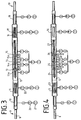
- FIG. 3 a vertical sputtering system is shown schematically in FIG. 3, which is used to apply a coating of ITO, silver and in turn ITO on a substrate at low substrate temperatures and for subsequent heat treatment (tempering).
- a transport carriage 8 with a U-shaped profile travels through such a sputtering system, which allows the substrates 4 shown in FIG. 2 to be attached to the two outer sides.
- the transport carriage 8 is introduced into a first insertion module 10. It then arrives in a second infeed module 11, where the substrates 4 are cleaned either by means of a plasma glow discharge or by briefly heating above 100 ° C.
- the trolleys 8 are then moved into a sputtering process chamber 12, where they are successively coated with ITO, metal and again ITO by sputtering with magnetron cathodes 13, 14, 15 and 13a, 14a, 15a.
- the partial pressure of the oxygen in the plasma of the magnetron cathodes 14 and 14a with a silver target must not exceed a certain value, since otherwise the layer properties of the silver layer are affected. Therefore, almost completely oxidized ITO targets must be used to sputter on the ITO layers, so that little or no addition of oxygen is necessary to achieve good layer properties.
- a target with 85 to 95 wt .-% In2O3 and 15 - 5 wt .-% SnO2 can be selected, a composition of 90 wt .-% In2O3 and 10 wt .-% SnO2 is preferred.
- the speed at which the transport carriage 8 with the substrates 4 in front of the magnetron cathodes 13, 14, 15; 13a, 14a, 15a along is the same in front of all magnetron cathodes. That is why the different layer thicknesses via the different sputtering rates of the magnetron cathodes 13, 14, 15; 13a, 14a, 15a. These sputtering rates can be set, among other things, via the DC or HF powers of the corresponding sputtering power supplies.
- the transport carriage 8 moves the substrates from the sputtering process chamber 12 and into a first discharge module 16, where the substrates 4 are heated up to 300 ° C. by means of a heater 17.
- the heater 17 engages in the U-shaped area of the transport carriage 8 and is therefore located between the substrates 4.
- Corresponding heaters are also provided in the second infeed module 11 and in the sputtering process chamber 12.
- the transport carriage 8 with the coated substrates moves out of the sputtering system via a second discharge module 18 and arrives at an unloading station 19. There, the coated substrates are removed from the transport carriage 8, which then returns to the loading station 9 to be loaded with new substrates there.
- the pumps required for the evacuation are also shown in Figure 3. While the first infeed module 10 and the second outfeed module 18 are only provided, for example, with a root pump 20 and a Trivac pump 21 as the backing pump system, in the second infeed module 11, the sputtering process chamber 12 and the first outfeed module 16, high vacuum pumps 22, for example turbomolecular pumps, are connected.
- the sputtering system according to FIG. 4 differs from that according to FIG. 3 in that the first discharge module 16 has no heating.
- the substrates are already heated to high temperatures of up to 300.degree.
- this temperature is maintained by means of central heating elements 24, 25, 26, 27.
- These heating elements 24, 25, 26, 27 and also the heater 23 protrude from above into a U-shaped bulge in the transport carriage 8 and thereby heat the substrates from behind. Otherwise, apart from the fact that the subsequent heat treatment is omitted, the process proceeds exactly as in the sputtering system according to FIG. 3.
- a further heater (not shown) can be installed on each wall in order to be able to heat up the substrates more quickly.
Landscapes
- Chemical & Material Sciences (AREA)
- Engineering & Computer Science (AREA)
- Chemical Kinetics & Catalysis (AREA)
- Materials Engineering (AREA)
- Organic Chemistry (AREA)
- Physics & Mathematics (AREA)
- General Chemical & Material Sciences (AREA)
- Geochemistry & Mineralogy (AREA)
- Life Sciences & Earth Sciences (AREA)
- General Physics & Mathematics (AREA)
- Optics & Photonics (AREA)
- Metallurgy (AREA)
- Nonlinear Science (AREA)
- Mechanical Engineering (AREA)
- Inorganic Chemistry (AREA)
- Crystallography & Structural Chemistry (AREA)
- Mathematical Physics (AREA)
- Physical Vapour Deposition (AREA)
- Laminated Bodies (AREA)
- Surface Treatment Of Glass (AREA)
Applications Claiming Priority (2)
| Application Number | Priority Date | Filing Date | Title |
|---|---|---|---|
| DE4239355A DE4239355A1 (de) | 1992-11-24 | 1992-11-24 | Transparentes Substrat mit einem transparenten Schichtsystem und Verfahren zur Herstellung eines solchen Schichtsystems |
| DE4239355 | 1992-11-24 |
Publications (1)
| Publication Number | Publication Date |
|---|---|
| EP0599071A1 true EP0599071A1 (fr) | 1994-06-01 |
Family
ID=6473449
Family Applications (1)
| Application Number | Title | Priority Date | Filing Date |
|---|---|---|---|
| EP93117383A Withdrawn EP0599071A1 (fr) | 1992-11-24 | 1993-10-27 | Substrat transparent avec un système de couches transparentes et procédé de production d'un tel système de couches |
Country Status (4)
| Country | Link |
|---|---|
| EP (1) | EP0599071A1 (fr) |
| JP (1) | JPH06199544A (fr) |
| KR (1) | KR940013303A (fr) |
| DE (1) | DE4239355A1 (fr) |
Cited By (15)
| Publication number | Priority date | Publication date | Assignee | Title |
|---|---|---|---|---|
| EP0676379A3 (fr) * | 1994-04-11 | 1996-05-01 | Saint Gobain Vitrage | Technique de fabrication d'une plaque de verre revêtue d'une couche d'argent semi-réfléchissante. |
| GB2300133A (en) * | 1995-04-27 | 1996-10-30 | Glaverbel | Coated substrate having high luminous transmission, low solar factor and neutral aspect in reflection. |
| DE19733053A1 (de) * | 1997-07-31 | 1999-02-04 | Leybold Ag | Transparentes Substrat |
| WO1999043626A1 (fr) * | 1998-02-25 | 1999-09-02 | Interpane Entwicklungs- Und Beratungsgesellschaft Mbh & Co. | Revetement thermoreflechissant, presentant une grande resistance thermique |
| EP1092689A1 (fr) | 1999-10-11 | 2001-04-18 | BPS Alzenau GmbH | Couches transparents et électroconductives et procédé pour leur déposition |
| EP1108693A1 (fr) * | 1999-12-06 | 2001-06-20 | Nippon Sheet Glass Co., Ltd. | Verre protegeant de la chaleur, procédé de fabrication et unité à multiple vitrage dans laquelle est utilisée ladite feuille de verre |
| DE10039412A1 (de) * | 2000-08-11 | 2002-02-21 | Balzers Process Systems Gmbh | Verfahren zur Herstellung eines Substrats mit einer transparenten, leitfähigen Beschichtung |
| WO2002076901A1 (fr) | 2001-03-27 | 2002-10-03 | Pilkington Deutschland Ag | Plaque de verre revetue |
| EP1130420A3 (fr) * | 1999-12-27 | 2002-11-27 | Nitto Denko Corporation | Laminé transparent, méthode de fabrication et panneau d'affichage à plasma |
| WO2002042806A3 (fr) * | 2000-11-22 | 2003-02-27 | Univ Stuttgart Inst Fuer Physi | Filtre uv a bande etroite pour detecteur uv |
| WO2002050579A3 (fr) * | 2000-12-20 | 2003-05-01 | Flabeg Gmbh & Co Kg | Procede de production d'un panneau additionnel pour ecrans plasma et panneau additionnel produit selon ce procede |
| WO2003068500A1 (fr) * | 2002-02-11 | 2003-08-21 | Ppg Industries Ohio, Inc. | Revetement contre le soleil |
| EP1518838A1 (fr) | 2003-09-24 | 2005-03-30 | Nippon Electric Glass Co., Ltd. | Article en verre |
| US20130171469A1 (en) * | 2012-01-04 | 2013-07-04 | Mke Technology Co. Ltd | Transparent conductive thin film |
| US12392023B1 (en) * | 2024-05-03 | 2025-08-19 | Applied Materials, Inc. | Methods and apparatus for depositing amorphous indium tin oxide film |
Families Citing this family (11)
| Publication number | Priority date | Publication date | Assignee | Title |
|---|---|---|---|---|
| DE4422439A1 (de) * | 1994-06-29 | 1996-01-11 | Flachglas Ag | Doppelglasscheibe für Mikrowellenöfen |
| US5667853A (en) * | 1995-03-22 | 1997-09-16 | Toppan Printing Co., Ltd. | Multilayered conductive film, and transparent electrode substrate and liquid crystal device using the same |
| DE19726966C1 (de) * | 1997-06-25 | 1999-01-28 | Flachglas Ag | Verfahren zur Herstellung einer transparenten Silberschicht mit hoher spezifischer elektrischer Leitfähigkeit , Glasscheibe mit einem Dünnschichtsystem mit einer solchen Silberschicht und deren Verwendung |
| KR100601669B1 (ko) | 2004-05-03 | 2006-07-14 | 삼성전자주식회사 | 현상기 및 이를 구비한 전자사진방식 화상형성장치 |
| FR2924723B1 (fr) * | 2007-12-11 | 2010-12-17 | Centre Nat Rech Scient | Support solide revetu d'au moins un film de metal et d'au moins une couche d'oxyde transparent et conducteur pour la detection par spr et/ou par une methode electrochimique |
| KR101172113B1 (ko) * | 2008-11-14 | 2012-08-10 | 엘지이노텍 주식회사 | 터치스크린 및 그 제조방법 |
| WO2014004518A1 (fr) * | 2012-06-26 | 2014-01-03 | Applied Materials, Inc. | Traitement thermique rapide par micro-ondes des dispositifs électrochimiques |
| US8766245B2 (en) | 2012-08-14 | 2014-07-01 | Guardian Industries Corp. | Organic light emitting diode with transparent electrode and method of making same |
| FR3038597B1 (fr) * | 2015-07-08 | 2021-12-10 | Saint Gobain | Materiau muni d'un empilement a proprietes thermiques |
| KR102629160B1 (ko) * | 2018-01-29 | 2024-01-29 | 어플라이드 머티어리얼스, 인코포레이티드 | 광학 디바이스 향상을 위한 습윤 층들 |
| DE102021132627A1 (de) | 2021-12-10 | 2023-06-15 | Schott Ag | Scheibenförmiger Glasartikel, Tür für einen Mikrowellenofen umfassend einen solchen Glasartikel sowie Mikrowellenofen |
Citations (5)
| Publication number | Priority date | Publication date | Assignee | Title |
|---|---|---|---|---|
| GB769697A (en) * | 1954-02-25 | 1957-03-13 | Ass Elect Ind | Improvements in the manufacture of transparent conducting films on transparent insulating backings |
| EP0229921A1 (fr) * | 1985-12-06 | 1987-07-29 | Leybold Aktiengesellschaft | Procédé de fabrication de vitres possédant une transmissivité dans le spectre visible et une réflexivité pour la chaleur rayonnante élevées |
| EP0281894A2 (fr) * | 1987-03-13 | 1988-09-14 | Flachglas Aktiengesellschaft | Procédé de fabrication d'une vitre de verre trempé et/ou bombé avec une couche d'argent, vitre ainsi fabriquée et son utilisation |
| WO1990011975A1 (fr) * | 1989-04-11 | 1990-10-18 | Andus Corporation | Revetements conducteurs transparents |
| EP0464789A1 (fr) * | 1990-07-05 | 1992-01-08 | Asahi Glass Company Ltd. | Film à faible émittance |
Family Cites Families (17)
| Publication number | Priority date | Publication date | Assignee | Title |
|---|---|---|---|---|
| FR2320565A1 (fr) * | 1973-04-12 | 1977-03-04 | Radiotechnique Compelec | Plaque a transparence selective et son procede de fabrication |
| DE2750500A1 (de) * | 1977-11-11 | 1979-05-17 | Leybold Heraeus Gmbh & Co Kg | Verfahren zur herstellung von infrarotreflektierenden, fuer sichtbares licht weitgehend transparenten scheiben und durch die verfahren hergestellte scheibe |
| JPS569249A (en) * | 1979-06-30 | 1981-01-30 | Sanyo Shinku Kogyo Kk | Electrically conductive infrared shielding glass and its manufacture |
| DE2930373A1 (de) * | 1979-07-26 | 1981-02-19 | Siemens Ag | Verfahren zum herstellen transparenter, elektrisch leitender indiumoxid (in tief 2 o tief 3 )-schichten |
| JPS57130303A (en) * | 1981-02-03 | 1982-08-12 | Sharp Kk | Method of producing transparent conductive film |
| DE3211066A1 (de) * | 1982-03-25 | 1983-09-29 | Siemens AG, 1000 Berlin und 8000 München | Transparente leitschicht |
| NO157212C (no) * | 1982-09-21 | 1988-02-10 | Pilkington Brothers Plc | Fremgangsmaate for fremstilling av belegg med lav emisjonsevne. |
| DE3307661A1 (de) * | 1983-03-04 | 1984-09-06 | Leybold-Heraeus GmbH, 5000 Köln | Verfahren zum herstellen von scheiben mit hohem transmissionsverhalten im sichtbaren spektralbereich und mit hohem reflexionsverhalten fuer waermestrahlung |
| DE3316548C2 (de) * | 1983-03-25 | 1985-01-17 | Flachglas AG, 8510 Fürth | Verfahren zur Beschichtung eines transparenten Substrates |
| DE3503851A1 (de) * | 1985-02-05 | 1986-08-07 | Interpane Entwicklungs- und Beratungsgesellschaft mbH & Co. KG, 3471 Lauenförde | Hochtransparenter in durch- und aussenansicht neutral wirkender und waermedaemmender belag |
| JPS6241740A (ja) * | 1985-08-19 | 1987-02-23 | Nippon Sheet Glass Co Ltd | 熱線反射ガラスの製造方法 |
| JPS63100043A (ja) * | 1986-10-15 | 1988-05-02 | Nippon Sheet Glass Co Ltd | 熱線反射ガラス |
| EP0299687B1 (fr) * | 1987-07-17 | 1993-06-23 | LUCAS INDUSTRIES public limited company | Objets transparents |
| US4883721A (en) * | 1987-07-24 | 1989-11-28 | Guardian Industries Corporation | Multi-layer low emissivity thin film coating |
| DE3825671A1 (de) * | 1987-08-08 | 1989-03-02 | Leybold Ag | Verfahren zum herstellen von scheiben mit hohem transmissionsverhalten im sichtbaren spektralbereich und mit hohem reflexionsverhalten fuer waermestrahlung sowie durch das verfahren hergestellte scheiben |
| CA1338926C (fr) * | 1988-07-27 | 1997-02-25 | Jun Kawaguchi | Panneau sandwich reflechissant la chaleur |
| DE4006804A1 (de) * | 1990-03-03 | 1991-09-05 | Renker Gmbh & Co Kg Zweigniede | Mehrschichtsystem mit hohem reflexionsvermoegen im infrarot-spektralbereich und mit hohem transmissionsvermoegen im sichtbaren bereich |
-
1992
- 1992-11-24 DE DE4239355A patent/DE4239355A1/de not_active Withdrawn
-
1993
- 1993-10-27 EP EP93117383A patent/EP0599071A1/fr not_active Withdrawn
- 1993-11-24 KR KR1019930025115A patent/KR940013303A/ko not_active Ceased
- 1993-11-24 JP JP5293115A patent/JPH06199544A/ja active Pending
Patent Citations (5)
| Publication number | Priority date | Publication date | Assignee | Title |
|---|---|---|---|---|
| GB769697A (en) * | 1954-02-25 | 1957-03-13 | Ass Elect Ind | Improvements in the manufacture of transparent conducting films on transparent insulating backings |
| EP0229921A1 (fr) * | 1985-12-06 | 1987-07-29 | Leybold Aktiengesellschaft | Procédé de fabrication de vitres possédant une transmissivité dans le spectre visible et une réflexivité pour la chaleur rayonnante élevées |
| EP0281894A2 (fr) * | 1987-03-13 | 1988-09-14 | Flachglas Aktiengesellschaft | Procédé de fabrication d'une vitre de verre trempé et/ou bombé avec une couche d'argent, vitre ainsi fabriquée et son utilisation |
| WO1990011975A1 (fr) * | 1989-04-11 | 1990-10-18 | Andus Corporation | Revetements conducteurs transparents |
| EP0464789A1 (fr) * | 1990-07-05 | 1992-01-08 | Asahi Glass Company Ltd. | Film à faible émittance |
Cited By (18)
| Publication number | Priority date | Publication date | Assignee | Title |
|---|---|---|---|---|
| EP0676379A3 (fr) * | 1994-04-11 | 1996-05-01 | Saint Gobain Vitrage | Technique de fabrication d'une plaque de verre revêtue d'une couche d'argent semi-réfléchissante. |
| GB2300133A (en) * | 1995-04-27 | 1996-10-30 | Glaverbel | Coated substrate having high luminous transmission, low solar factor and neutral aspect in reflection. |
| GB2300133B (en) * | 1995-04-27 | 1998-07-29 | Glaverbel | Coated substrate having high luminous transmission, low solar factor and neutral aspect in reflection |
| DE19733053A1 (de) * | 1997-07-31 | 1999-02-04 | Leybold Ag | Transparentes Substrat |
| WO1999043626A1 (fr) * | 1998-02-25 | 1999-09-02 | Interpane Entwicklungs- Und Beratungsgesellschaft Mbh & Co. | Revetement thermoreflechissant, presentant une grande resistance thermique |
| EP1092689A1 (fr) | 1999-10-11 | 2001-04-18 | BPS Alzenau GmbH | Couches transparents et électroconductives et procédé pour leur déposition |
| EP1108693A1 (fr) * | 1999-12-06 | 2001-06-20 | Nippon Sheet Glass Co., Ltd. | Verre protegeant de la chaleur, procédé de fabrication et unité à multiple vitrage dans laquelle est utilisée ladite feuille de verre |
| US6855369B2 (en) | 1999-12-27 | 2005-02-15 | Nitto Denko Corporation | Transparent laminate, method for producing the same, and plasma display panel |
| EP1130420A3 (fr) * | 1999-12-27 | 2002-11-27 | Nitto Denko Corporation | Laminé transparent, méthode de fabrication et panneau d'affichage à plasma |
| DE10039412A1 (de) * | 2000-08-11 | 2002-02-21 | Balzers Process Systems Gmbh | Verfahren zur Herstellung eines Substrats mit einer transparenten, leitfähigen Beschichtung |
| WO2002042806A3 (fr) * | 2000-11-22 | 2003-02-27 | Univ Stuttgart Inst Fuer Physi | Filtre uv a bande etroite pour detecteur uv |
| WO2002050579A3 (fr) * | 2000-12-20 | 2003-05-01 | Flabeg Gmbh & Co Kg | Procede de production d'un panneau additionnel pour ecrans plasma et panneau additionnel produit selon ce procede |
| WO2002076901A1 (fr) | 2001-03-27 | 2002-10-03 | Pilkington Deutschland Ag | Plaque de verre revetue |
| WO2003068500A1 (fr) * | 2002-02-11 | 2003-08-21 | Ppg Industries Ohio, Inc. | Revetement contre le soleil |
| EP1518838A1 (fr) | 2003-09-24 | 2005-03-30 | Nippon Electric Glass Co., Ltd. | Article en verre |
| US20130171469A1 (en) * | 2012-01-04 | 2013-07-04 | Mke Technology Co. Ltd | Transparent conductive thin film |
| US8642166B2 (en) * | 2012-01-04 | 2014-02-04 | Mke Technology Co., Ltd. | Transparent conductive thin film |
| US12392023B1 (en) * | 2024-05-03 | 2025-08-19 | Applied Materials, Inc. | Methods and apparatus for depositing amorphous indium tin oxide film |
Also Published As
| Publication number | Publication date |
|---|---|
| JPH06199544A (ja) | 1994-07-19 |
| DE4239355A1 (de) | 1994-05-26 |
| KR940013303A (ko) | 1994-06-25 |
Similar Documents
| Publication | Publication Date | Title |
|---|---|---|
| EP0599071A1 (fr) | Substrat transparent avec un système de couches transparentes et procédé de production d'un tel système de couches | |
| DE69915350T2 (de) | Verfahren und vorrichtung zur herstellung von beschichtungen auf basis von silber mit niedrigem strahlungsvermögen ohne metallprimer | |
| EP1092689B1 (fr) | Couches transparents et électroconductives et procédé pour leur déposition | |
| DE68913068T2 (de) | Neutrale kathodenzerstäubte Metallegierungsoxidfilme. | |
| DE3687336T2 (de) | Durchsichtiger gegenstand mit einer hohen sichtbaren durchlaessigkeit. | |
| DE68915042T2 (de) | Film mit geringerer Emission für Hochtemperaturbehandlung. | |
| EP0281894B1 (fr) | Procédé de fabrication d'une vitre de verre trempé et/ou bombé avec une couche d'argent, vitre ainsi fabriquée et son utilisation | |
| EP0224704B1 (fr) | Procédé de fabrication d'une vitre trempée et/ou bombée avec une transmission réduite | |
| DE69526191T2 (de) | Geglühte Beschichtung mit niedrigem Strahlungsvermögen | |
| DE69418542T2 (de) | Verfahren zur Herstellung funktioneller Beschichtungen | |
| DE69404690T2 (de) | Glassubstrate beschichtet mit einer Häufung von dünnen Schichten, Anwendung für Glasscheiben mit Infrarot reflectierenden Eigenschaften und/oder mit sonnenstrahlungseigenschaften | |
| DE69920278T2 (de) | Verglasungsscheibe | |
| EP0999192B1 (fr) | Système isolant thermique de couches | |
| DE69027590T2 (de) | Verfahren zur Herstellung von Schichten auf basis von Siliziumdioxyd mittels DC Sputtern und Target dafür | |
| DE69701582T2 (de) | Durchsichtiges Substrat mit einem Dünnschichtaufbau mit Eigenschaften im Infrarotgebiet | |
| EP0436045B1 (fr) | Procédé de fabrication d'une plaque de verre trempée ou bombée à revêtement sur la face arrière, vitre ainsi fabriquée et son utilisation | |
| DE4024308A1 (de) | Waermeisolierglas mit dielektrischem vielschichtenueberzug | |
| DE69713663T2 (de) | Oxidfilm, Laminate und Verfahren zu deren Herstellung | |
| DE2750500A1 (de) | Verfahren zur herstellung von infrarotreflektierenden, fuer sichtbares licht weitgehend transparenten scheiben und durch die verfahren hergestellte scheibe | |
| DE8907490U1 (de) | Fassadenplatte | |
| EP1538131B1 (fr) | Empilement multicouche à basse émissivité trempable, procédé pour la fabrication et produit en verre à basse émissivité avec systeme multicouche | |
| DE102009051796A1 (de) | Thermisch belastbares Schichtsystem | |
| DE3503851A1 (de) | Hochtransparenter in durch- und aussenansicht neutral wirkender und waermedaemmender belag | |
| DE69510886T2 (de) | Transparentes Substrat mit einer Häufung von Schichten aus Silber, Verwendung als heizbare Verbundglasscheibe | |
| DE69804866T2 (de) | Hitzebiegbare spiegel |
Legal Events
| Date | Code | Title | Description |
|---|---|---|---|
| PUAI | Public reference made under article 153(3) epc to a published international application that has entered the european phase |
Free format text: ORIGINAL CODE: 0009012 |
|
| AK | Designated contracting states |
Kind code of ref document: A1 Designated state(s): CH DE FR GB LI NL |
|
| STAA | Information on the status of an ep patent application or granted ep patent |
Free format text: STATUS: THE APPLICATION IS DEEMED TO BE WITHDRAWN |
|
| 18D | Application deemed to be withdrawn |
Effective date: 19941202 |