EP0599181A2 - Spannungsfühler - Google Patents
Spannungsfühler Download PDFInfo
- Publication number
- EP0599181A2 EP0599181A2 EP93118477A EP93118477A EP0599181A2 EP 0599181 A2 EP0599181 A2 EP 0599181A2 EP 93118477 A EP93118477 A EP 93118477A EP 93118477 A EP93118477 A EP 93118477A EP 0599181 A2 EP0599181 A2 EP 0599181A2
- Authority
- EP
- European Patent Office
- Prior art keywords
- voltage
- pockels cell
- polarizer
- modulation
- measured
- Prior art date
- Legal status (The legal status is an assumption and is not a legal conclusion. Google has not performed a legal analysis and makes no representation as to the accuracy of the status listed.)
- Granted
Links
Images


Classifications
-
- G—PHYSICS
- G01—MEASURING; TESTING
- G01R—MEASURING ELECTRIC VARIABLES; MEASURING MAGNETIC VARIABLES
- G01R19/00—Arrangements for measuring currents or voltages or for indicating presence or sign thereof
-
- G—PHYSICS
- G01—MEASURING; TESTING
- G01R—MEASURING ELECTRIC VARIABLES; MEASURING MAGNETIC VARIABLES
- G01R15/00—Details of measuring arrangements of the types provided for in groups G01R17/00 - G01R29/00, G01R33/00 - G01R33/26 or G01R35/00
- G01R15/14—Adaptations providing voltage or current isolation, e.g. for high-voltage or high-current networks
- G01R15/24—Adaptations providing voltage or current isolation, e.g. for high-voltage or high-current networks using light-modulating devices
- G01R15/241—Adaptations providing voltage or current isolation, e.g. for high-voltage or high-current networks using light-modulating devices using electro-optical modulators, e.g. electro-absorption
- G01R15/242—Adaptations providing voltage or current isolation, e.g. for high-voltage or high-current networks using light-modulating devices using electro-optical modulators, e.g. electro-absorption based on the Pockels effect, i.e. linear electro-optic effect
Definitions
- the present invention relates to a voltage sensor that is used in an optical PT (Power Transformer) that detects a voltage to ground or a voltage of a driving power source for motors and the like.
- optical PT Power Transformer
- An intensity-modulated voltage sensor arranges, for example, as shown in Fig. 10, along the optical axis, successively from the side of incident light, a first polarizer 35 of set angle 90 degrees, a 1/4 wavelength plate 38, a Pockels cell 2, and a second polarizer 36 of set angle 95 degrees, and a voltage to be measured is applied to Pockels cell 2. Since a change in the output intensity of second polarizer corresponds to the polarization state of the output light of Pockels cell 2, which varies depending on voltage to be measured, the voltage to be measured can be determined by monitoring the change in the output power of polarizer with an optical receiver.
- the modulation depth of an output power is defined as the ratio of the AC component of the output power to the DC component of the output power.
- the object of the present invention is therefore to solve the problem described above in a prior intensity-modulated voltage sensor and to provide a voltage sensor that performs the measurement from DC to high-frequency AC with its simple composition and without being influenced by the external environment.
- the present invention provides a voltage sensor composed by arranging along an optical axis, successively from the side of incident light, a first polarizer, a Pockels cell for detection, a Pockels cell for modulation, and a second polarizer.
- An electric field proportional to the voltage to be measured is applied to the Pockels cell for detection.
- a periodic electric field for modulation that varies the difference of phase angles by 2n ⁇ radians, where n is a positive integer, during each period and that has a frequency higher than the electric field applied to the Pockels cell for detection is applied to the Pockels cell for modulation.
- the voltage sensor detects the voltage to be measured from a phase change in the intensity of the light having passed through the second polarizer.
- the voltage to be measured is determined for a wide range from DC to high frequency without being influenced by the external environment.
- Fig. 1 shows a diagram of a voltage sensor of a first embodiment of the present invention
- Figs. 2, 3, 4 and 5 show a block diagram of the first embodiment, and the graphs of changes in the voltages V and V m applied to Pockels cells and an output power P from the second polarizer.
- the voltage sensor comprises a first polarizer 1 of set angle 90 degrees, a Pockels cell 2 for detection whose set angle ⁇ of the major axis 14 to a horizontal axis 11 thereof is 45 degrees, a Pockels cell 3 for modulation whose major axis is parallel to that of Pockels cell 2 for detection, and a second polarizer 4 of set angle 90 degrees successively arranged in this order from the side of incident light along an optical axis 14.
- a periodic electric field E m for modulation that varies the difference of phase angles by 2n ⁇ radians, where n is a positive integer, during each period and that has a much higher frequency than that of magnetic field E applied to Pockels cell 2 for detection is applied to Pockels cell 3 for modulation with a periodic voltage V m for modulation.
- Pockels cell 2 for detection and Pockels cell 3 for modulation is made of LiNbO3.
- Unpolarized incident light 6 is changed by first polarizer 1 into linearly polarized light 7, which after passing through Pockels cell 2 for detection becomes elliptically polarized light 8 owing to phase angle ⁇ of Pockels cell 2 for detection and, after passing through Pockels cell 3 for modulation, becomes elliptically polarized light 9, which corresponds to the sum ⁇ + ⁇ m of the difference of phase angles ⁇ due to Pockels cell 2 for detection and the difference of phase angles ⁇ m due to Pockels cell 3 for modulation.
- the intensity of linearly polarized light 10, which results from passing through second polarizer 4 shows a change in the intensity proportional to ⁇ cos( ⁇ m + ⁇ ) + 1 ⁇ ⁇ 2 from the intensity of the incident light.
- a signal analyzer 5 for optical calculation compares the phase change ⁇ + ⁇ m of above output 10 with the phase difference ⁇ m of the Pockels cell 3 for modulation to calculate the phase difference ⁇ due to Pockels cell 2 for detection, and determines the voltage to be measured.
- the set angle of each device is an angle with respect to a base angle as indicated by a reference number 11 in Fig. 1, and the angle is measured in units of radians.
- Fig. 2 shows a block diagram of the first embodiment.
- an electric field E for detection is generated by electrodes couple 17 for detection to which voltage to be measured V is applied.
- an electric field E m for modulation is generated by electrodes couple 18 to which periodic voltage V m for modulation is applied.
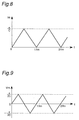
- voltage V to be measured has a sine waveform of amplitude a, frequency f, and initial phase angle ⁇ , as shown in Fig. 3.
- Voltage V m for modulation has a sawtooth waveform of modulation frequency f m and varies linearly with slope 2 ⁇ x f m /C during each period of 1/f m , as shown in Fig. 4.
- constant C is the proportional coefficient between a voltage for modulation and the phase difference of the Pockels cell 3 for modulation.
- phase difference ⁇ which is due to the Pockels cell 2 for detection and proportional to voltage V to be measured, as indicated by a solid line 29 in Fig. 5.
- the waveform of output P of polarizer 4 is changed from the dotted line 28 to the solid line 29 when the voltage V to be detected is applied to Pockels cell 2 for detection.
- signal analyzer 5 for optical calculation demodulates voltage to be measured V proportional to the phase difference ⁇ due to Pockels cell 2 for detection from the phase change ⁇ + ⁇ m of output 10.
- the signal analyzer 5 is comprised of a photo-electric converter 5A for converting the output 10 of the second polarizer 4 into a voltage proportional thereto, a demodulator 5B for demodulating an output of the converter 5A and an integrator 5C for integrating an output of the demodulator 5B.
- modulation frequency f m is required to be sufficiently higher than the frequency f of voltage V to be measured. If voltage V to be measured is of commercial frequency, modulation frequency f m of about 1 kHz is sufficient.
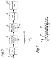
- a second embodiment of the present invention is described with reference to Figs. 6 and 7.
- the second embodiment is the same as the first embodiment in that a first polarizer 1, a Pockels cell 2 for detection, a Pockels cell 3 for modulation, and a second polarizer 4 are arranged in this order along the optical axis of the voltage sensor.
- an integrator 14 that inputs a voltage V to be measured to itself and performs an integrating operation to output an electric field E for detection is inserted between Pockels cell 2 for detection and an input terminal for voltage V to be measured.
- obtaining electric field E that varies by a change equivalent to the integral value of voltage V to be measured suffices.
- the input to integrator 14 may be an electric field proportional to voltage V to be measured.
- the output of polarizer 4 changes in the frequency from a sine wave 31 corresponding to the variation of the phase difference ⁇ m of the Pockels cell 3 for modulation, which is proportional to periodic voltage V m for modulation, by an amount proportional to the phase difference ⁇ of the Pockels cell 2 for detection, which is proportional to voltage V to be measured, as shown in Fig. 7.
- the result is a frequency-modulated waveform 32.
- signal analyzer 30 for optical calculation demodulates frequency-modulated waveform 32 to obtain voltage V to be measured proportional to the phase difference ⁇ of the Pockels cell 2 for detection.
- a voltage is measured through a phase change or a frequency change in intensity modulated light
- the measurement can be performed without being influenced by essential problems in dealing with an optical transmission channel such as a change in the loss of connection in an optical part or a change in light intensity due to the external environment.
- information other than that of the voltage to be measured is not mixed with the phase change or the frequency change, consideration of the distinction between the voltage to be measured and the other external influences in measuring a near DC voltage through an intensity change by a prior method becomes unnecessary, so that the measurement can be performed by a consistent method for voltages from DC to AC.
- the directions of the first polarizer and the second polarizer are arbitrary. If the two directions are parallel or perpendicular to each other, then apart from a sawtooth waveform that varies the phase difference by 2n ⁇ radians, where n is a positive integer, during each period as shown in Fig. 4, voltage V m for modulation that varies the phase difference by n ⁇ from k ⁇ to (k + n) ⁇ , where k is an integer, suffices, so that voltage V m for modulation can be made small. Further, as shown in Fig. 8, the waveform of voltage V m for modulation can be made isosceles triangular unlike the sawtooth waveform shown in Fig. 4, where the phase difference ⁇ m is varied rapidly in a neighborhood of 2(k + n) ⁇ radians, so that the turbulence of the output wave occurs less.
- the phase difference ⁇ m can be varied from k ⁇ + ⁇ /2 to (k + n) ⁇ + ⁇ /2, where k is an integer and n is a positive integer, suffices.
- first and second embodiments detect a voltage using a phase change or temporary phase change (frequency) in output power
- the set angles of first polarizer 1 and second polarizer 4 can be arbitrary so far as they are inclined by 45 degrees from the major axis of the Pockels cells.
- the first and second embodiments arranged Pockels cell 2 for detection and Pockels cell 3 for modulation from the incident side of light in this order. However, the order may be the opposite.
- first polarizer 1 Pockels cell 2 for detection, Pockels cell 3 for modulation, and second polarizer 4 can not be arranged in the same optical axis, such as when first polarizer 1 or Pockels cell 3 for modulation or second polarizer 4 is installed in another apparatus, then an optical transmission channel such as a polarization maintaining fiber where the polarization state is not changed can be used between neighboring devices of first polarizer 1, Pockels cell 2 for detection, Pockels cell 3 for modulation, and second polarizer 4 such that the distance between them is far-or the optical axes differ.
- an optical transmission channel such as a polarization maintaining fiber where the polarization state is not changed can be used between neighboring devices of first polarizer 1, Pockels cell 2 for detection, Pockels cell 3 for modulation, and second polarizer 4 such that the distance between them is far-or the optical axes differ.
- the present invention has the effect of detecting a voltage to be measured from DC to high frequency without being influenced by the external environment.
Landscapes
- Physics & Mathematics (AREA)
- General Physics & Mathematics (AREA)
- Measuring Instrument Details And Bridges, And Automatic Balancing Devices (AREA)
Applications Claiming Priority (2)
| Application Number | Priority Date | Filing Date | Title |
|---|---|---|---|
| JP312203/92 | 1992-11-20 | ||
| JP31220392 | 1992-11-20 |
Publications (3)
| Publication Number | Publication Date |
|---|---|
| EP0599181A2 true EP0599181A2 (de) | 1994-06-01 |
| EP0599181A3 EP0599181A3 (de) | 1995-03-08 |
| EP0599181B1 EP0599181B1 (de) | 1998-09-02 |
Family
ID=18026453
Family Applications (1)
| Application Number | Title | Priority Date | Filing Date |
|---|---|---|---|
| EP93118477A Expired - Lifetime EP0599181B1 (de) | 1992-11-20 | 1993-11-16 | Spannungsfühler |
Country Status (5)
| Country | Link |
|---|---|
| US (1) | US5477134A (de) |
| EP (1) | EP0599181B1 (de) |
| KR (1) | KR100201022B1 (de) |
| DE (1) | DE69320763T2 (de) |
| TW (1) | TW224513B (de) |
Cited By (3)
| Publication number | Priority date | Publication date | Assignee | Title |
|---|---|---|---|---|
| EP0696739A3 (de) * | 1994-08-12 | 1997-03-05 | Matsushita Electric Industrial Co Ltd | Optischer Fühler |
| EP1447890A1 (de) * | 2003-02-12 | 2004-08-18 | Northrop Grumman Corporation | Laserspiegel mit variabler Spiegelung |
| DE19716477B4 (de) * | 1997-03-05 | 2011-11-10 | Areva T&D Sa | Verfahren und Einrichtung zur Messung einer elektrischen Spannung |
Families Citing this family (6)
| Publication number | Priority date | Publication date | Assignee | Title |
|---|---|---|---|---|
| US6252388B1 (en) | 1998-12-04 | 2001-06-26 | Nxtphase Corporation | Method and apparatus for measuring voltage using electric field sensors |
| JP2000258465A (ja) * | 1999-03-09 | 2000-09-22 | Hitachi Ltd | 光電圧センサ |
| US6380725B1 (en) | 2000-02-15 | 2002-04-30 | Nxtphase Corporation | Voltage sensor |
| JP2004093257A (ja) * | 2002-08-30 | 2004-03-25 | Oki Electric Ind Co Ltd | 光センサユニット |
| WO2005026751A1 (en) * | 2003-09-05 | 2005-03-24 | Blake James N | Time division multiplexed optical measuring system |
| KR102251284B1 (ko) * | 2020-11-27 | 2021-05-12 | 국방과학연구소 | 광학 소자를 이용하여 전압을 측정하기 위한 장치 및 방법 |
Family Cites Families (8)
| Publication number | Priority date | Publication date | Assignee | Title |
|---|---|---|---|---|
| US3584949A (en) * | 1968-12-04 | 1971-06-15 | Richard G Clow | Optical computing apparatus and method |
| JPS5647723A (en) * | 1979-09-27 | 1981-04-30 | Nippon Hoso Kyokai <Nhk> | Rotation measuring method for light phase and plane of polarization |
| JPS5918923A (ja) * | 1982-07-23 | 1984-01-31 | Toshiba Corp | 複屈折測定装置 |
| JPS5990061A (ja) * | 1983-07-01 | 1984-05-24 | Masahiko Inoue | コンデンサ形計器用変圧器の出力信号伝送装置 |
| JPH06100619B2 (ja) * | 1985-12-24 | 1994-12-12 | 松下電器産業株式会社 | 光フアイバ応用センサ |
| US5111135A (en) * | 1989-07-12 | 1992-05-05 | Ngk Insulators, Ltd. | Method for optically measuring electric field and optical voltage/electric-field sensor |
| JP2986503B2 (ja) * | 1990-03-09 | 1999-12-06 | 株式会社日立製作所 | 光方式直流電圧変成器 |
| US5134361A (en) * | 1991-02-19 | 1992-07-28 | The United States Of America As Represented By The Secretary Of The Navy | Opitcal system for linearizing non-linear electro-optic |
-
1993
- 1993-07-20 TW TW082105778A patent/TW224513B/zh active
- 1993-11-16 DE DE69320763T patent/DE69320763T2/de not_active Expired - Fee Related
- 1993-11-16 US US08/152,234 patent/US5477134A/en not_active Expired - Lifetime
- 1993-11-16 EP EP93118477A patent/EP0599181B1/de not_active Expired - Lifetime
- 1993-11-19 KR KR1019930024686A patent/KR100201022B1/ko not_active Expired - Fee Related
Cited By (5)
| Publication number | Priority date | Publication date | Assignee | Title |
|---|---|---|---|---|
| EP0696739A3 (de) * | 1994-08-12 | 1997-03-05 | Matsushita Electric Industrial Co Ltd | Optischer Fühler |
| US5635829A (en) * | 1994-08-12 | 1997-06-03 | Matsushita Electric Industrial Co., Ltd. | Optical sensor |
| DE19716477B4 (de) * | 1997-03-05 | 2011-11-10 | Areva T&D Sa | Verfahren und Einrichtung zur Messung einer elektrischen Spannung |
| EP1447890A1 (de) * | 2003-02-12 | 2004-08-18 | Northrop Grumman Corporation | Laserspiegel mit variabler Spiegelung |
| US7173956B2 (en) | 2003-02-12 | 2007-02-06 | Northrop Grumman Corporation | Electrically controlled uniform or graded reflectivity electro-optic mirror |
Also Published As
| Publication number | Publication date |
|---|---|
| TW224513B (de) | 1994-06-01 |
| KR100201022B1 (ko) | 1999-06-15 |
| DE69320763T2 (de) | 1999-01-14 |
| EP0599181B1 (de) | 1998-09-02 |
| KR940011956A (ko) | 1994-06-22 |
| US5477134A (en) | 1995-12-19 |
| EP0599181A3 (de) | 1995-03-08 |
| DE69320763D1 (de) | 1998-10-08 |
Similar Documents
| Publication | Publication Date | Title |
|---|---|---|
| CA1208452A (en) | Device for measuring a phase shift, which is not reciprocal, produced in a ring interferometer | |
| US4629323A (en) | Birefringence type measuring device | |
| US6952107B2 (en) | Optical electric field or voltage sensing system | |
| EP0351171B1 (de) | Verfahren und Anordnung zur optischen Messung von elektrischen und magnetischen Grössen | |
| GB2125960A (en) | Measuring magnetic field | |
| US5477134A (en) | Voltage sensor for use in optical power transformer including a pair of Pockels cells | |
| US6204954B1 (en) | Technique for measuring the Vpi-AC of a mach-zehnder modulator | |
| Hidaka et al. | Simultaneous measurement of two orthogonal components of electric field using a Pockels device | |
| EP0691758B1 (de) | Synchrone Detektion von optischen Signalen | |
| UA35606C2 (uk) | Спосіб вимірювання пропускання, кругового дихроїзму, оптичного обертання оптично активних речовин та дихрограф для його здійснення | |
| JPH08146066A (ja) | 電気信号測定方法および装置 | |
| EP0598356A2 (de) | Polarisationszustands-Detektor und ihn verwendender Stromsensor | |
| US5495100A (en) | Phase difference detecting method, circuit and apparatus | |
| Ookubo et al. | A New Method of Dynamic Electric Birefringence Measurement Using a Sinusoidal Digital Lock-In System | |
| KR100228416B1 (ko) | 광(光)을 이용한 일체형 전류/전압 측정장치 | |
| JPH06207954A (ja) | 電圧センサ | |
| JP3179316B2 (ja) | 光センサ | |
| RU2112937C1 (ru) | Поляриметр | |
| SU1182410A1 (ru) | Устройство дл бесконтактного измерени силы тока | |
| JPH07140181A (ja) | 電圧センサ | |
| SU789758A1 (ru) | Магнитооптический измерительный преобразователь | |
| Funck et al. | A new AC–DC transfer device for high voltages and high frequencies using electrooptic modulation | |
| JPH10111320A (ja) | 光電圧・光電流センサ | |
| JP3201729B2 (ja) | 光センサシステムの使用方法 | |
| JPH06207858A (ja) | 偏光状態検出器およびそれを用いた電流センサ |
Legal Events
| Date | Code | Title | Description |
|---|---|---|---|
| PUAI | Public reference made under article 153(3) epc to a published international application that has entered the european phase |
Free format text: ORIGINAL CODE: 0009012 |
|
| 17P | Request for examination filed |
Effective date: 19931116 |
|
| AK | Designated contracting states |
Kind code of ref document: A2 Designated state(s): DE FR GB |
|
| PUAL | Search report despatched |
Free format text: ORIGINAL CODE: 0009013 |
|
| AK | Designated contracting states |
Kind code of ref document: A3 Designated state(s): DE FR GB |
|
| 17Q | First examination report despatched |
Effective date: 19970707 |
|
| GRAG | Despatch of communication of intention to grant |
Free format text: ORIGINAL CODE: EPIDOS AGRA |
|
| GRAH | Despatch of communication of intention to grant a patent |
Free format text: ORIGINAL CODE: EPIDOS IGRA |
|
| GRAH | Despatch of communication of intention to grant a patent |
Free format text: ORIGINAL CODE: EPIDOS IGRA |
|
| GRAA | (expected) grant |
Free format text: ORIGINAL CODE: 0009210 |
|
| AK | Designated contracting states |
Kind code of ref document: B1 Designated state(s): DE FR GB |
|
| REF | Corresponds to: |
Ref document number: 69320763 Country of ref document: DE Date of ref document: 19981008 |
|
| ET | Fr: translation filed | ||
| PLBE | No opposition filed within time limit |
Free format text: ORIGINAL CODE: 0009261 |
|
| STAA | Information on the status of an ep patent application or granted ep patent |
Free format text: STATUS: NO OPPOSITION FILED WITHIN TIME LIMIT |
|
| 26N | No opposition filed | ||
| REG | Reference to a national code |
Ref country code: GB Ref legal event code: IF02 |
|
| PGFP | Annual fee paid to national office [announced via postgrant information from national office to epo] |
Ref country code: DE Payment date: 20071108 Year of fee payment: 15 |
|
| PGFP | Annual fee paid to national office [announced via postgrant information from national office to epo] |
Ref country code: GB Payment date: 20071114 Year of fee payment: 15 Ref country code: FR Payment date: 20071108 Year of fee payment: 15 |
|
| GBPC | Gb: european patent ceased through non-payment of renewal fee |
Effective date: 20081116 |
|
| REG | Reference to a national code |
Ref country code: FR Ref legal event code: ST Effective date: 20090731 |
|
| PG25 | Lapsed in a contracting state [announced via postgrant information from national office to epo] |
Ref country code: DE Free format text: LAPSE BECAUSE OF NON-PAYMENT OF DUE FEES Effective date: 20090603 |
|
| PG25 | Lapsed in a contracting state [announced via postgrant information from national office to epo] |
Ref country code: GB Free format text: LAPSE BECAUSE OF NON-PAYMENT OF DUE FEES Effective date: 20081116 |
|
| PG25 | Lapsed in a contracting state [announced via postgrant information from national office to epo] |
Ref country code: FR Free format text: LAPSE BECAUSE OF NON-PAYMENT OF DUE FEES Effective date: 20081130 |