EP0599409A2 - Récepteur à conversion directe - Google Patents
Récepteur à conversion directe Download PDFInfo
- Publication number
- EP0599409A2 EP0599409A2 EP93203232A EP93203232A EP0599409A2 EP 0599409 A2 EP0599409 A2 EP 0599409A2 EP 93203232 A EP93203232 A EP 93203232A EP 93203232 A EP93203232 A EP 93203232A EP 0599409 A2 EP0599409 A2 EP 0599409A2
- Authority
- EP
- European Patent Office
- Prior art keywords
- signal
- direct conversion
- conversion receiver
- data
- valid data
- Prior art date
- Legal status (The legal status is an assumption and is not a legal conclusion. Google has not performed a legal analysis and makes no representation as to the accuracy of the status listed.)
- Granted
Links
Images

Classifications
-
- H—ELECTRICITY
- H03—ELECTRONIC CIRCUITRY
- H03J—TUNING RESONANT CIRCUITS; SELECTING RESONANT CIRCUITS
- H03J7/00—Automatic frequency control; Automatic scanning over a band of frequencies
- H03J7/02—Automatic frequency control
-
- H—ELECTRICITY
- H04—ELECTRIC COMMUNICATION TECHNIQUE
- H04B—TRANSMISSION
- H04B1/00—Details of transmission systems, not covered by a single one of groups H04B3/00 - H04B13/00; Details of transmission systems not characterised by the medium used for transmission
- H04B1/06—Receivers
- H04B1/16—Circuits
- H04B1/30—Circuits for homodyne or synchrodyne receivers
-
- H—ELECTRICITY
- H03—ELECTRONIC CIRCUITRY
- H03D—DEMODULATION OR TRANSFERENCE OF MODULATION FROM ONE CARRIER TO ANOTHER
- H03D3/00—Demodulation of angle-, frequency- or phase- modulated oscillations
- H03D3/02—Demodulation of angle-, frequency- or phase- modulated oscillations by detecting phase difference between two signals obtained from input signal
- H03D3/04—Demodulation of angle-, frequency- or phase- modulated oscillations by detecting phase difference between two signals obtained from input signal by counting or integrating cycles of oscillations
-
- H—ELECTRICITY
- H03—ELECTRONIC CIRCUITRY
- H03D—DEMODULATION OR TRANSFERENCE OF MODULATION FROM ONE CARRIER TO ANOTHER
- H03D7/00—Transference of modulation from one carrier to another, e.g. frequency-changing
- H03D7/16—Multiple-frequency-changing
- H03D7/165—Multiple-frequency-changing at least two frequency changers being located in different paths, e.g. in two paths with carriers in quadrature
Definitions
- the present invention relates to a direct conversion receiver comprising a local frequency generating arrangement which is coupled to a pair of quadrature related mixers for mixing down an rf input signal to quadrature related signals, a demodulator for demodulating the quadrature related signals into demodulated data, and a.f.c. means for providing a control signal for the local frequency generating arrangement, the a.f.c. means being coupled to quadrature paths.
- Such direct conversion receivers can be digital paging receivers or transceivers using an FSK (Frequency Shift Keying) modulation scheme, but also transceivers for cordless telephony or the like.
- a direct conversion receiver of this kind is known from the British Patent Application GB 2 180 419.
- an a.f.c. (automatic frequency control) signal for a local oscillator with inherent correct polarity is derived from so-called I- and Q-channel receiver paths.
- a baseband I-channel signal is fed to a phase detector, together with a Q-channel signal, which is also fed to a frequency discriminator.
- Output signals of the phase detector and the frequency discriminator are fed to a multiplier, an output of which providing the control signal, which is fed to the local oscillator via a low pass filter as a loop filter.
- the a.f.c. means are complex in that a closed loop a.f.c.
- a direct conversion receiver is characterized in that the a.f.c. means comprise a digital-to-analog conversion arrangement for providing the control signal, signal quality determining means for determining a valid data signal from the demodulated data, storage means for storing a valid data range during scanning intervals, and means for adjusting an output signal of the digital-to-analog conversion arrangement to an adjustment value within the valid data range.
- a very simple a.f.c. means is achieved, a loop filter being dispensed with.
- the a.f.c. means essentially is based upon open loop control, the control signal being updated from time to time, preferably on a regular basis.
- the valid data range is obtained.
- the present invention is based upon the insight that such scanning need not be repeated very often, temperature drift or aging being slow processes.
- WO 92/08294 discloses an a.f.c. for a superheterodyne receiver having a digital-to-analog converter for supplying a control signal to a local oscillator, but this a.f.c. essentially is a digital closed loop a.f.c., i.e. a closed loop error signal is computed on the basis of a measured offset frequency. Furthermore, a separate RSSI circuit (Received Signal Strength Indication) is necessary, the disclosed method only working for strong signals.
- RSSI circuit Receiveived Signal Strength Indication
- the adjustment value is a value around a mid-range value within the valid data range. In this way a more reliable adjustment value is obtained as would be obtained more at the boundaries of the valid data range where transition from valid to unvalid data occurs more easily, with oscillator drift.
- a first range is scanned, and in a second operating mode a second, limited, range is scanned around a previous adjustment value. It is achieved that frequency scanning time is reduced once an operating point has been adjusted previously.
- valid data scanning is halted during expected data frames. It is achieved, when scanning overlaps expected data frames, that these data frames are not lost. In practice, for robust detection of valid data, such overlap would occur. Thus, the scanning can be done in between data frames.
- the signal quality determining means comprise a frequency-to-voltage converter coupled to an analog-to-digital conversion arrangement or to a comparison arrangement, for determining the valid data signal.
- the signal quality is determined on the basis of a threshold of operation with respect to BER (bit error rate).
- the signal frequency at the threshold of operation can be differentiated from the frequency of a noise signal alone, i.e. where no data are present.
- the signal quality determining means comprise a microcontroller coupled to a gated counter for determining the valid data signal.
- the control signal value is preferably chosen such that a minimum counter value is achieved, corresponding to a mid-range value within the valid data range.
- the signal quality determining means determine the valid data signal on the basis of signal characteristics of the demodulated data, such as a valid CRC, a CRC with a unique error syndrome, a data frame preamble, a sync pattern, or a BER.
- the acronym CRC means Cyclic Redundancy Code
- the acronym BER means Bit Error Rate.
- a microcontroller is to be used, evaluating the signal characteristics. Detection of the signal characteristics can be done according to relevant standards, e.g. the POGSAG paging standard.
- the local frequency generating arrangement comprises a thermally insulated crystal. It is achieved that a period between consecutive scans is prolonged. Especially in a direct conversion communication device as a handheld device, usually being powered by means of batteries, this leads to battery saving.
- a further embodiment of a direct conversion receiver according to the present invention is characterized in that the receiver comprises first a.f.c. means as claimed in any one of the claims 1 to 11, second a.f.c. means particularly suitable for relatively strong rf input signals, and RSSI-means for determining a signal strength of the input signal, the direct conversion communication being arranged for switching over from the first to the second a.f.c. means if the determined signal strength exceeds a predetermined threshold value.
- An optimal a.f.c. means is thus achieved.
- the first a.f.c. means are optimised for relatively low rf input signal power
- the second a.f.c. means are optimised for relatively high rf input power, leading to an overall optimal a.f.c. performance.
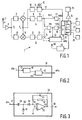
- FIG. 1 schematically shows a direct conversion receiver 1 according to the present invention.
- the direct conversion receiver 1 which can be a paging transceiver, comprises an antenna 2 for receiving an rf (radio frequency) input signal rf, which can be an rf FSK (Frequency Shift Keying) signal carrying FSK modulated digital signals.
- the rf input signal rf is fed to a low noise rf amplifier 3, which is coupled to quadrature paths 4 and 5, so-called I- and Q-channels, for mixing down the rf input signal rf to quadrature related signals I and Q.
- the quadrature path 4 comprises a phase shifting device 6 causing a +45 degrees phase shift of the amplified rf signal.
- the phase shifting device 6 is coupled to a mixer 7 for mixing down the rf signal rf to the signal I, an output of the mixer 7 being filtered and limited by means of a respective filter 8 and a limiter 9.
- the quadrature path 5 comprises a phase shifting device 10 causing a -45 degrees phase shift of the amplified rf signal, a mixer 11, a filter 12, and a limiter 13 for achieving the signal Q.
- the filters 8 and 12 are provided for limiting the noise bandwidth and for channel selectivity. By AC-coupling of the filters 8 and 12 to the mixers 7 and 11, DC-offset effects are avoided.
- the limiters 9 and 13 are provided for removing amplitude signal variations.
- the mixers 7 and 11 are further coupled to a local frequency generating arrangement 14, e.g. a crystal oscillator having a crystal 15 as a frequency determining element, via a frequency multiplication arrangement 16.
- the local frequency generating arrangement 14 can also be a more elaborate arrangement, e.g. a frequency sysnthesizer having a crystal oscillator for providing a reference frequency.
- Such frequency synthesizers can operate on the basis of a PLL (phase locked loop).
- the mixing frequency i.e. an output frequency f L of the multiplication arrangement 16, further denoted as oscillator frequency, is chosen such that zero intermediate-frequency signals I and Q are obtained, with respect to a carrier frequency f c .
- a single 90 degrees phase shifting device can be applied, for phase shifting the oscillator signal for one of mixer signals.
- a frequency offset of the oscillator frequency f L with respect to the rf input signal rf i.e.
- the direct conversion receiver 1 comprises a demodulator 18 to which the quadrature related signals I and Q are fed.
- the demodulator 18 can be a lead-lag phase detector for demodulating FSK data.
- the demodulator 18 is coupled via a data filter 19 to a microcontroller 20 with RAM and ROM memory 21 and 22 and an I/O-interface 23. Such microcontrollers are well known in the art.
- the demodulator 18 provides demodulated data dta, and the data filter 19 provides filtered demodulated data fdta.
- various output signals may be provided for such as a speech signal via an amplifier 24 and a speech reproducing device 25, an information message via a display unit 26, a audible tone signal via a bleeper 27, and a visual alert signal via an LED 28.
- transmission means 29 are provided for sending a return message, which means 29 are controlled by the microcontroller 20, the transmission means being coupled to a transmitting aerial 29.
- the direct conversion receiver 1 comprises a.f.c.
- a digital-to-analog conversion arrangement 31 for providing a control signal ct for the local oscillator 14, signal quality determining means 32 for determining a valid data signal vdta from the demodulated data dta, from the filtered demodulated data fdta, from one of the signals I and Q, i.e. from an output signal of the limiter 9 or 13, or from a product of the signals I and Q, storage means for storing a valid data range during scanning intervals, the storage means being the RAM memory 21 e.g., and means for adjusting the output signal ct of the digital-to-analog conversion arrangement 31 to an adjustment value within the valid data range.
- the signal quality determining means 32 determine the quality of the received signal rf for a stepping range of the digital-to-analog conversion means 31, the stepping being controlled by the microcontroller 20, during scanning intervals.
- the microcontroller 20 determines a valid data range and adjusts the control signal ct to an adjustment value within the valid data range, preferably a mid-range value.
- the scanning preferably is at regular intervals, e.g. every 5 or 10 minutes.
- the scanning can be interrupted in case of overlap with expected data frames, an old adjustement value still being used as the control signal ct.
- a whole output range of the digital-to-analog conversion can be stepped, whereas in a second mode, after an initial first scanning, only a limited stepping can be done around an operating point of the control signal ct, being the last adjustment value obtained during a previous scanning.
- a no signal or weak signal condition during normal data reception intervals, there is no need to start the scanning procedure immediately, since such condition could be due to signal fading, or even due to an interruption of signal transmission. If during regular scanning no valid data is detected, the scanning could be repeated more often. In between scanning intervals, normal reception could be tried using the last adjustment value of the control signal ct.
- the present invention allows for quite higher data rates as with known paging receivers, since the offset frequency is made very small by the a.f.c. means.
- the signal quality determining means 32 can be implemented in hardware or software, in the latter case stored in the ROM memory 22.
- the digital-to-analog conversion arrangement 31 can be built into the microcontroller 20, as shown, but can also be a separate device.
- the a.f.c. means can be implemented as a separate IC (Integrated Circuit).
- Integrated Circuit Integrated Circuit
- the present invention allows for using crystals without temperature compensation.
- the crystal 15 is thermally insulated. Such insulation as such is well known in the art. A lot of heat transfer from the crystal to the environment thereof occurs via electrical connection leads of the crystal. By applying long connection leads which are helically wounded while at the same time insulated, a good heat insulation is obtained.
- Fig. 2 shows an embodiment of the signal quality determining means 32 according to the present invention, the same reference numerals having been used for corresponding features.
- the signal quality determining means 32 comprise a frequency-to-voltage converter 40 coupled to a comparator 41 of which an output 42 provides the valid data signal vdta, e.g. a logic "0" signal representing valid data, and a logic "1" signal representing invalid data.
- the demodulated data dta can be applied, as shown, but also the filtered demodulated data fdta, one of the quadrature related signals I or Q, being output signals of the limiters 9 and 13, or the product if the signals I and Q.
- Fig. 3 shows an embodiment of the frequency-to-voltage converter 40 in signal quality determining means 32 according to the present invention.
- the frequency-to-voltage converter 40 comprises an opamp 50 with a plus input 51 coupled to ground, and with a parallel arrangement of a resistor 52 and a capacitor 53 coupled between a minus input 54 and an output 55 of the opamp 50, the output 55 being an output 56 of the frequency-to-voltage converter 40.
- Coupled between an input 57 of the frequency-to-voltage converter 40 and the input 54 is a series arrangement of a capacitor 58 and a diode 59, and between a connection point 60 of the capacitor 58 and the diode 59 a diode 61 connected to ground.
- the converter 40 operates as a diode-pump frequency indicator on digital input data.
- the determination of a valid data signal is based upon the idea that the presence of a signal can be distinguished from noise alone or a too bad signal from BER (Bit Error Rate) point of view.
- BER Bit Error Rate
- Distinction between valid or invalid data is made by comparing an output of the frequency-to-voltage converter 40 with a threshold value thr, if the comparator 41 is used.
- an analog-to-digital converter can be used, which then provides digital values to the microcontroller 20. In the latter case, the microcontroller 20 determines the valid data signal vdta.
- Fig. 4 shows another embodiment of the signal quality determining means 32 according to the present invention, comprising a gated counter 70 coupled with a counter output 71, and with a gate input 72 to the microcontroller 20, which provides the control signal ct.
- the demodulated data dta as shown, or the filtered demodulated data fdta, or one of the signals I or Q, or the product of the signals I and Q, is fed to a counter input 73.
- the counter exhibits a range of output values around a minimum counter value, whereas higher counter values correspond to invalid data. It has been shown that use of limiter output data gives a more reliable valid data determination, use of demodulated data possibly giving rise to local minima at which an incorrect decision can be made.
- Fig. 5 shows ranges of an output of the digital-to-analog converter 31 according to the present invention. Shown are a full output voltage range DAR of the digital-to-analog conversion arrangement 31, scanned during the first operating mode, a valid data range VR during a scanning interval, and a limited range LR, scanned during the second operating mode.
- an adjustment value for the control signal ct is chosen as a mid-range value or in the vicinity thereof, as it should be realized that there is no sharp transition between valid and invalid data at edges of the valid data range VR.
- the limited range LR is preferably centered around the adjustment value set during the first operating mode.
- Fig. 6 shows frequencies of signals according to the present invention. Shown are the (fictitious) carrier frequency f C , the oscillator frequency f L , a frequency deviation ⁇ f of data "0" and data “1" FSK modulated signals with respect to the fictitious carrier frequency f C , a frequency offset ⁇ f of the oscillator frequency f L with respect to the carrier frequency f C , and f0 and f1 signals, representing demodulated signals for data "0" and data "1", respectively.
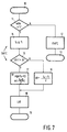
- Fig. 7 shows a flow chart for second a.f.c. means in a direct conversion communication device according to the present invention, which are embodied by means of a stored program in the ROM 22 of the microcontroller 20.
- the described a.f.c. means according to the present invention form first a.f.c. means.
- a further embodiment of a direct conversion communication device 1 according to the present invention is arranged for switching over from the first a.f.c. means to the second a.f.c. means and vice versa on the basis of the signal strength of the input signal rf.
- the direct conversion receiver is provided with RSSI-means (Received Signal Strength Indication), which can be conventional RSSI-means (not shown), or a gated counter such as described in relation to figure 4. In the latter case the signal strength is determined on the basis of the frequency of a counter input signal, being the signal I or Q, or the product of the signals I and Q.
- RSSI-means Received Signal Strength Indication
- a conventional analog RSSI-signal can be obtained from one of the limiters 9 and 13, which analog RSSI-signal can then be compared with a predetermined threshold value thr1 by means of a comparator 33.
- An output signal sdta of the comparator 33 indicating that the limiter signal is above the threshold value thr1, ie.
- a relatively strong signal is fed to the microcontroller 20, implementing the second a.f.c. means.
- the microcontroller switches over from the first to the second a.f.c. means on the basis of the signal sdta.
- the second a.f.c. means are now described with the help of the flow chart of figure 6. Shown is a program begin block 10. In a test block 11, the stored program in the ROM 22 tests the signal sdta. If the signal sdta has got a logical value "1", corresponding to a relatively strong rf input signal, the microcontroller 20 switches over to the second a.f.c. means, being particularly optimized for strong input sigals rt.
- the microcontroller 20 controls the first a.f.c. means, as described, indicated with an acronym FAFC, meaning First A.F.C. means, i.e. the valid data scanning according to the present invention, in block 12.
- the program routine then ends with an end block 13.
- a test block 15 it is tested if f1 > 2 ⁇ f' or f0 > 2 ⁇ f', i.e. whether
- > ⁇ f. It is to be noticed that ⁇ f' ⁇ ⁇ f, whereby the exact value of ⁇ f' depends on an applied pre-modulation de-emphasis. If the condition in block 15 is not true, i.e. an in-range situation applies, ⁇ f is calculated in block 16, according to ⁇ f (f0-f1)/2 . If the condition in block 15 is true, i.e.
- ⁇ f is calculated in block 17, according to [sign(f0-f1)]*[(f0+f1) ⁇ 2] , sign being the well known mathematical sign function.
- the microcontroller determines an input value for the digital-to-analog conversion arrangement 31, providing the control signal ct, the input value e.g. being determined by applying the calculated frequency offset value ⁇ f as an address value for a lookup table LUT in the ROM 22, the lookup table LUT comprising digital representations of control values ct.
- the lookup-table can be filled with data reflecting a known or measured a.f.c. behaviour of the direct conversion device 1.
- the first and second a.f.c. means can be optimised such that an overall a.f.c. performance is approximately linear with the signal power of the input signal rf.
Landscapes
- Engineering & Computer Science (AREA)
- Computer Networks & Wireless Communication (AREA)
- Signal Processing (AREA)
- Digital Transmission Methods That Use Modulated Carrier Waves (AREA)
Priority Applications (1)
| Application Number | Priority Date | Filing Date | Title |
|---|---|---|---|
| EP19930203232 EP0599409B1 (fr) | 1992-11-26 | 1993-11-18 | Récepteur à conversion directe |
Applications Claiming Priority (3)
| Application Number | Priority Date | Filing Date | Title |
|---|---|---|---|
| EP92203648 | 1992-11-26 | ||
| EP92203648 | 1992-11-26 | ||
| EP19930203232 EP0599409B1 (fr) | 1992-11-26 | 1993-11-18 | Récepteur à conversion directe |
Publications (3)
| Publication Number | Publication Date |
|---|---|
| EP0599409A2 true EP0599409A2 (fr) | 1994-06-01 |
| EP0599409A3 EP0599409A3 (en) | 1995-11-08 |
| EP0599409B1 EP0599409B1 (fr) | 2003-02-12 |
Family
ID=26131817
Family Applications (1)
| Application Number | Title | Priority Date | Filing Date |
|---|---|---|---|
| EP19930203232 Expired - Lifetime EP0599409B1 (fr) | 1992-11-26 | 1993-11-18 | Récepteur à conversion directe |
Country Status (1)
| Country | Link |
|---|---|
| EP (1) | EP0599409B1 (fr) |
Cited By (7)
| Publication number | Priority date | Publication date | Assignee | Title |
|---|---|---|---|---|
| WO1997014158A3 (fr) * | 1995-10-11 | 1997-05-09 | Philips Electronics Nv | Circuit recepteur |
| US5633898A (en) * | 1993-12-22 | 1997-05-27 | Matsushita Electric Industrial Co., Ltd. | Automatic frequency control apparatus for FSK receiver and FSK receiver including the same |
| GB2332311A (en) * | 1997-12-12 | 1999-06-16 | Nec Corp | AFC in FSK receiver |
| US6148047A (en) * | 1998-05-06 | 2000-11-14 | Philips Electronics North America Corporation | DC offset compensation for zero if quadrature demodulator |
| US6766148B1 (en) * | 2000-03-21 | 2004-07-20 | Koninklijke Phillips Electronics N.V. | Switched sideband frequency low-IF transmitter |
| KR100466471B1 (ko) * | 1996-03-19 | 2005-05-24 | 코닌클리케 필립스 일렉트로닉스 엔.브이. | 집적수신기 |
| US8768408B2 (en) | 1998-11-26 | 2014-07-01 | Nokia Corporation | Method and arrangement for transmitting and receiving RF signals through various radio interfaces of communication systems |
Family Cites Families (2)
| Publication number | Priority date | Publication date | Assignee | Title |
|---|---|---|---|---|
| GB2180419A (en) * | 1985-09-16 | 1987-03-25 | Philips Electronic Associated | Direct conversion receiver |
| FI91821C (fi) * | 1991-02-22 | 1994-08-10 | Nokia Mobile Phones Ltd | Radiopuhelimen automaattinen taajuudensäätökytkentä |
-
1993
- 1993-11-18 EP EP19930203232 patent/EP0599409B1/fr not_active Expired - Lifetime
Cited By (13)
| Publication number | Priority date | Publication date | Assignee | Title |
|---|---|---|---|---|
| US5633898A (en) * | 1993-12-22 | 1997-05-27 | Matsushita Electric Industrial Co., Ltd. | Automatic frequency control apparatus for FSK receiver and FSK receiver including the same |
| KR100470008B1 (ko) * | 1995-10-11 | 2005-05-27 | 코닌클리케 필립스 일렉트로닉스 엔.브이. | 수신기회로 |
| US5953643A (en) * | 1995-10-11 | 1999-09-14 | U.S. Philips Corporation | Receiver circuit |
| WO1997014158A3 (fr) * | 1995-10-11 | 1997-05-09 | Philips Electronics Nv | Circuit recepteur |
| KR100466471B1 (ko) * | 1996-03-19 | 2005-05-24 | 코닌클리케 필립스 일렉트로닉스 엔.브이. | 집적수신기 |
| GB2332311A (en) * | 1997-12-12 | 1999-06-16 | Nec Corp | AFC in FSK receiver |
| GB2332311B (en) * | 1997-12-12 | 2000-01-26 | Nec Corp | Automatic frequency control in FSK receiver |
| US6332007B1 (en) | 1997-12-12 | 2001-12-18 | Nec Corporation | Automatic frequency control in FSK receiver using voltage window deviation |
| US6148047A (en) * | 1998-05-06 | 2000-11-14 | Philips Electronics North America Corporation | DC offset compensation for zero if quadrature demodulator |
| US8768408B2 (en) | 1998-11-26 | 2014-07-01 | Nokia Corporation | Method and arrangement for transmitting and receiving RF signals through various radio interfaces of communication systems |
| US8838049B1 (en) | 1998-11-26 | 2014-09-16 | Nokia Corporation | Method and arrangement for transmitting and receiving RF signals through various radio interfaces of communication systems |
| US9270301B2 (en) | 1998-11-26 | 2016-02-23 | Nokia Technologies Oy | Method and arrangement for transmitting and receiving RF signals through various radio interfaces of communication systems |
| US6766148B1 (en) * | 2000-03-21 | 2004-07-20 | Koninklijke Phillips Electronics N.V. | Switched sideband frequency low-IF transmitter |
Also Published As
| Publication number | Publication date |
|---|---|
| EP0599409A3 (en) | 1995-11-08 |
| EP0599409B1 (fr) | 2003-02-12 |
Similar Documents
| Publication | Publication Date | Title |
|---|---|---|
| US5438692A (en) | Direct conversion receiver | |
| US5584068A (en) | Direct conversion receiver | |
| EP0394064B1 (fr) | Récepteur à conversion directe avec une fréquence porteuse locale présentant une gigue pour la détection d'une fréquence porteuse transmise | |
| US4816769A (en) | BPSK demodulator and FM receiver for digital data pagers | |
| US6195400B1 (en) | Two-mode demodulating apparatus | |
| US6070062A (en) | Mobile radio wave receiver with adaptive automatic gain control | |
| EP1835628B1 (fr) | Recepteur et transmetteur sans fil | |
| US6034990A (en) | Digital radio transmission and reception system applying a direct modulation and demodulation method | |
| EP0478238A2 (fr) | Système et procédé de contrôle automatique de fréquence pour systèmes de transmission à sauts de fréquence | |
| US5701600A (en) | Radio receiver and method of calibrating same | |
| KR100427854B1 (ko) | 주파수 안정화된 송/수신 회로 | |
| US6240147B1 (en) | Auto frequency control apparatus | |
| EP0599409B1 (fr) | Récepteur à conversion directe | |
| AU670896B2 (en) | Automatic frequency control circuit | |
| US7359448B2 (en) | Remote transmitter system and method | |
| EP0866575B1 (fr) | Calibrage de fréquence à base de microcontrôleur | |
| HK1019024A (en) | A direct conversion receiver | |
| JPH07297779A (ja) | 自動周波数制御機能を備えたディジタル無線機 | |
| EP0599414B1 (fr) | Récepteur à conversion directe | |
| JP3833259B2 (ja) | Fsk受信器における周波数制御信号の生成 | |
| GB2287144A (en) | A radio device | |
| US6621879B1 (en) | Digital radio system, a digital radio device, and a quadrature demodulator | |
| HK1012803B (en) | A direct conversion receiver | |
| WO1987004311A1 (fr) | Procede de communication de donnees par radio et dispositif pour la mise en oeuvre du procede | |
| JPH0260263A (ja) | 無線機に用いる局部発振器の周波数安定化回路 |
Legal Events
| Date | Code | Title | Description |
|---|---|---|---|
| PUAI | Public reference made under article 153(3) epc to a published international application that has entered the european phase |
Free format text: ORIGINAL CODE: 0009012 |
|
| AK | Designated contracting states |
Kind code of ref document: A2 Designated state(s): CH DE FR GB IT LI |
|
| RAP1 | Party data changed (applicant data changed or rights of an application transferred) |
Owner name: N.V. PHILIPS' GLOEILAMPENFABRIEKEN |
|
| PUAL | Search report despatched |
Free format text: ORIGINAL CODE: 0009013 |
|
| AK | Designated contracting states |
Kind code of ref document: A3 Designated state(s): CH DE FR GB IT LI |
|
| 17P | Request for examination filed |
Effective date: 19960508 |
|
| RAP3 | Party data changed (applicant data changed or rights of an application transferred) |
Owner name: KONINKLIJKE PHILIPS ELECTRONICS N.V. |
|
| 17Q | First examination report despatched |
Effective date: 19990903 |
|
| GRAG | Despatch of communication of intention to grant |
Free format text: ORIGINAL CODE: EPIDOS AGRA |
|
| GRAG | Despatch of communication of intention to grant |
Free format text: ORIGINAL CODE: EPIDOS AGRA |
|
| GRAH | Despatch of communication of intention to grant a patent |
Free format text: ORIGINAL CODE: EPIDOS IGRA |
|
| GRAH | Despatch of communication of intention to grant a patent |
Free format text: ORIGINAL CODE: EPIDOS IGRA |
|
| GRAA | (expected) grant |
Free format text: ORIGINAL CODE: 0009210 |
|
| AK | Designated contracting states |
Designated state(s): CH DE FR GB IT LI |
|
| PG25 | Lapsed in a contracting state [announced via postgrant information from national office to epo] |
Ref country code: LI Free format text: LAPSE BECAUSE OF FAILURE TO SUBMIT A TRANSLATION OF THE DESCRIPTION OR TO PAY THE FEE WITHIN THE PRESCRIBED TIME-LIMIT Effective date: 20030212 Ref country code: IT Free format text: LAPSE BECAUSE OF FAILURE TO SUBMIT A TRANSLATION OF THE DESCRIPTION OR TO PAY THE FEE WITHIN THE PRE;WARNING: LAPSES OF ITALIAN PATENTS WITH EFFECTIVE DATE BEFORE 2007 MAY HAVE OCCURRED AT ANY TIME BEFORE 2007. THE CORRECT EFFECTIVE DATE MAY BE DIFFERENT FROM THE ONE RECORDED.SCRIBED TIME-LIMIT Effective date: 20030212 Ref country code: CH Free format text: LAPSE BECAUSE OF FAILURE TO SUBMIT A TRANSLATION OF THE DESCRIPTION OR TO PAY THE FEE WITHIN THE PRESCRIBED TIME-LIMIT Effective date: 20030212 |
|
| REG | Reference to a national code |
Ref country code: GB Ref legal event code: FG4D |
|
| REG | Reference to a national code |
Ref country code: CH Ref legal event code: EP |
|
| REG | Reference to a national code |
Ref country code: GB Ref legal event code: 746 Effective date: 20030219 |
|
| REF | Corresponds to: |
Ref document number: 69332685 Country of ref document: DE Date of ref document: 20030320 Kind code of ref document: P |
|
| ET | Fr: translation filed | ||
| REG | Reference to a national code |
Ref country code: CH Ref legal event code: PL |
|
| REG | Reference to a national code |
Ref country code: FR Ref legal event code: D6 |
|
| PLBE | No opposition filed within time limit |
Free format text: ORIGINAL CODE: 0009261 |
|
| 26N | No opposition filed |
Effective date: 20031113 |
|
| REG | Reference to a national code |
Ref country code: HK Ref legal event code: WD Ref document number: 1019024 Country of ref document: HK |
|
| REG | Reference to a national code |
Ref country code: GB Ref legal event code: 732E |
|
| REG | Reference to a national code |
Ref country code: GB Ref legal event code: 732E |
|
| REG | Reference to a national code |
Ref country code: FR Ref legal event code: TP |
|
| REG | Reference to a national code |
Ref country code: FR Ref legal event code: GC |
|
| REG | Reference to a national code |
Ref country code: GB Ref legal event code: 732E Free format text: REGISTERED BETWEEN 20090618 AND 20090624 |
|
| REG | Reference to a national code |
Ref country code: FR Ref legal event code: GC |
|
| PGFP | Annual fee paid to national office [announced via postgrant information from national office to epo] |
Ref country code: DE Payment date: 20091112 Year of fee payment: 17 |
|
| PGFP | Annual fee paid to national office [announced via postgrant information from national office to epo] |
Ref country code: GB Payment date: 20091118 Year of fee payment: 17 Ref country code: FR Payment date: 20091123 Year of fee payment: 17 |
|
| REG | Reference to a national code |
Ref country code: GB Ref legal event code: 732E Free format text: REGISTERED BETWEEN 20101007 AND 20101013 |
|
| GBPC | Gb: european patent ceased through non-payment of renewal fee |
Effective date: 20101118 |
|
| REG | Reference to a national code |
Ref country code: FR Ref legal event code: ST Effective date: 20110801 |
|
| REG | Reference to a national code |
Ref country code: FR Ref legal event code: GC |
|
| PG25 | Lapsed in a contracting state [announced via postgrant information from national office to epo] |
Ref country code: DE Free format text: LAPSE BECAUSE OF NON-PAYMENT OF DUE FEES Effective date: 20110531 |
|
| PG25 | Lapsed in a contracting state [announced via postgrant information from national office to epo] |
Ref country code: FR Free format text: LAPSE BECAUSE OF NON-PAYMENT OF DUE FEES Effective date: 20101130 |
|
| PG25 | Lapsed in a contracting state [announced via postgrant information from national office to epo] |
Ref country code: GB Free format text: LAPSE BECAUSE OF NON-PAYMENT OF DUE FEES Effective date: 20101118 |
|
| REG | Reference to a national code |
Ref country code: DE Ref legal event code: R119 Ref document number: 69332685 Country of ref document: DE Effective date: 20110601 Ref country code: DE Ref legal event code: R119 Ref document number: 69332685 Country of ref document: DE Effective date: 20110531 |
|
| REG | Reference to a national code |
Ref country code: FR Ref legal event code: AU Effective date: 20120126 |