EP0600382A2 - Tête d'impression à jet d'encre - Google Patents
Tête d'impression à jet d'encre Download PDFInfo
- Publication number
- EP0600382A2 EP0600382A2 EP93119039A EP93119039A EP0600382A2 EP 0600382 A2 EP0600382 A2 EP 0600382A2 EP 93119039 A EP93119039 A EP 93119039A EP 93119039 A EP93119039 A EP 93119039A EP 0600382 A2 EP0600382 A2 EP 0600382A2
- Authority
- EP
- European Patent Office
- Prior art keywords
- ink
- spacer
- pressure generating
- recording head
- type recording
- Prior art date
- Legal status (The legal status is an assumption and is not a legal conclusion. Google has not performed a legal analysis and makes no representation as to the accuracy of the status listed.)
- Granted
Links
- 125000006850 spacer group Chemical group 0.000 claims abstract description 72
- 239000000758 substrate Substances 0.000 claims abstract description 58
- 238000005530 etching Methods 0.000 claims abstract description 51
- 239000013078 crystal Substances 0.000 claims abstract description 44
- 238000005192 partition Methods 0.000 claims abstract description 29
- XUIMIQQOPSSXEZ-UHFFFAOYSA-N Silicon Chemical compound [Si] XUIMIQQOPSSXEZ-UHFFFAOYSA-N 0.000 claims abstract description 25
- 229910052710 silicon Inorganic materials 0.000 claims abstract description 25
- 239000010703 silicon Substances 0.000 claims abstract description 25
- 238000000638 solvent extraction Methods 0.000 claims abstract description 19
- 239000000853 adhesive Substances 0.000 claims description 37
- VYPSYNLAJGMNEJ-UHFFFAOYSA-N Silicium dioxide Chemical compound O=[Si]=O VYPSYNLAJGMNEJ-UHFFFAOYSA-N 0.000 claims description 25
- 230000008859 change Effects 0.000 claims description 8
- NJPPVKZQTLUDBO-UHFFFAOYSA-N novaluron Chemical compound C1=C(Cl)C(OC(F)(F)C(OC(F)(F)F)F)=CC=C1NC(=O)NC(=O)C1=C(F)C=CC=C1F NJPPVKZQTLUDBO-UHFFFAOYSA-N 0.000 claims description 5
- 229910052814 silicon oxide Inorganic materials 0.000 claims description 5
- 230000001154 acute effect Effects 0.000 claims description 3
- 238000006073 displacement reaction Methods 0.000 abstract description 3
- 238000000034 method Methods 0.000 description 15
- 239000000377 silicon dioxide Substances 0.000 description 10
- 235000012239 silicon dioxide Nutrition 0.000 description 10
- 230000001681 protective effect Effects 0.000 description 8
- KRHYYFGTRYWZRS-UHFFFAOYSA-N Fluorane Chemical compound F KRHYYFGTRYWZRS-UHFFFAOYSA-N 0.000 description 7
- 239000012530 fluid Substances 0.000 description 6
- 239000000463 material Substances 0.000 description 6
- NLKNQRATVPKPDG-UHFFFAOYSA-M potassium iodide Chemical compound [K+].[I-] NLKNQRATVPKPDG-UHFFFAOYSA-M 0.000 description 6
- 230000008569 process Effects 0.000 description 6
- 239000007864 aqueous solution Substances 0.000 description 4
- HSJPMRKMPBAUAU-UHFFFAOYSA-N cerium(3+);trinitrate Chemical compound [Ce+3].[O-][N+]([O-])=O.[O-][N+]([O-])=O.[O-][N+]([O-])=O HSJPMRKMPBAUAU-UHFFFAOYSA-N 0.000 description 4
- 238000007639 printing Methods 0.000 description 4
- 239000000243 solution Substances 0.000 description 4
- KWYUFKZDYYNOTN-UHFFFAOYSA-M Potassium hydroxide Chemical compound [OH-].[K+] KWYUFKZDYYNOTN-UHFFFAOYSA-M 0.000 description 3
- 229910000040 hydrogen fluoride Inorganic materials 0.000 description 3
- 229910052751 metal Inorganic materials 0.000 description 3
- 239000002184 metal Substances 0.000 description 3
- 238000000206 photolithography Methods 0.000 description 3
- 229920005989 resin Polymers 0.000 description 3
- 239000011347 resin Substances 0.000 description 3
- ZCYVEMRRCGMTRW-UHFFFAOYSA-N 7553-56-2 Chemical compound [I] ZCYVEMRRCGMTRW-UHFFFAOYSA-N 0.000 description 2
- VYZAMTAEIAYCRO-UHFFFAOYSA-N Chromium Chemical compound [Cr] VYZAMTAEIAYCRO-UHFFFAOYSA-N 0.000 description 2
- MHAJPDPJQMAIIY-UHFFFAOYSA-N Hydrogen peroxide Chemical compound OO MHAJPDPJQMAIIY-UHFFFAOYSA-N 0.000 description 2
- 230000008901 benefit Effects 0.000 description 2
- 230000015572 biosynthetic process Effects 0.000 description 2
- 229910052804 chromium Inorganic materials 0.000 description 2
- 239000011651 chromium Substances 0.000 description 2
- 238000000576 coating method Methods 0.000 description 2
- 230000008602 contraction Effects 0.000 description 2
- 230000000694 effects Effects 0.000 description 2
- 229920006332 epoxy adhesive Polymers 0.000 description 2
- PCHJSUWPFVWCPO-UHFFFAOYSA-N gold Chemical compound [Au] PCHJSUWPFVWCPO-UHFFFAOYSA-N 0.000 description 2
- 239000010931 gold Substances 0.000 description 2
- 229910052737 gold Inorganic materials 0.000 description 2
- 239000011630 iodine Substances 0.000 description 2
- 229910052740 iodine Inorganic materials 0.000 description 2
- 238000010030 laminating Methods 0.000 description 2
- 230000003647 oxidation Effects 0.000 description 2
- 238000007254 oxidation reaction Methods 0.000 description 2
- 230000009467 reduction Effects 0.000 description 2
- 238000007650 screen-printing Methods 0.000 description 2
- DDFHBQSCUXNBSA-UHFFFAOYSA-N 5-(5-carboxythiophen-2-yl)thiophene-2-carboxylic acid Chemical compound S1C(C(=O)O)=CC=C1C1=CC=C(C(O)=O)S1 DDFHBQSCUXNBSA-UHFFFAOYSA-N 0.000 description 1
- MIMUSZHMZBJBPO-UHFFFAOYSA-N 6-methoxy-8-nitroquinoline Chemical compound N1=CC=CC2=CC(OC)=CC([N+]([O-])=O)=C21 MIMUSZHMZBJBPO-UHFFFAOYSA-N 0.000 description 1
- GRYLNZFGIOXLOG-UHFFFAOYSA-N Nitric acid Chemical compound O[N+]([O-])=O GRYLNZFGIOXLOG-UHFFFAOYSA-N 0.000 description 1
- 239000003082 abrasive agent Substances 0.000 description 1
- 230000009471 action Effects 0.000 description 1
- 230000001070 adhesive effect Effects 0.000 description 1
- 239000000956 alloy Substances 0.000 description 1
- 229910045601 alloy Inorganic materials 0.000 description 1
- 238000004891 communication Methods 0.000 description 1
- 239000000470 constituent Substances 0.000 description 1
- 238000005260 corrosion Methods 0.000 description 1
- 230000007797 corrosion Effects 0.000 description 1
- 230000001419 dependent effect Effects 0.000 description 1
- 238000001704 evaporation Methods 0.000 description 1
- 230000008020 evaporation Effects 0.000 description 1
- 238000010438 heat treatment Methods 0.000 description 1
- 230000005764 inhibitory process Effects 0.000 description 1
- 239000000203 mixture Substances 0.000 description 1
- 229910017604 nitric acid Inorganic materials 0.000 description 1
- 239000002245 particle Substances 0.000 description 1
- 238000000059 patterning Methods 0.000 description 1
- 238000003825 pressing Methods 0.000 description 1
- 230000004044 response Effects 0.000 description 1
- 238000000926 separation method Methods 0.000 description 1
- 238000004544 sputter deposition Methods 0.000 description 1
- 239000004575 stone Substances 0.000 description 1
- 239000000126 substance Substances 0.000 description 1
- 230000003746 surface roughness Effects 0.000 description 1
Images


Classifications
-
- B—PERFORMING OPERATIONS; TRANSPORTING
- B41—PRINTING; LINING MACHINES; TYPEWRITERS; STAMPS
- B41J—TYPEWRITERS; SELECTIVE PRINTING MECHANISMS, i.e. MECHANISMS PRINTING OTHERWISE THAN FROM A FORME; CORRECTION OF TYPOGRAPHICAL ERRORS
- B41J2/00—Typewriters or selective printing mechanisms characterised by the printing or marking process for which they are designed
- B41J2/005—Typewriters or selective printing mechanisms characterised by the printing or marking process for which they are designed characterised by bringing liquid or particles selectively into contact with a printing material
- B41J2/01—Ink jet
- B41J2/135—Nozzles
- B41J2/16—Production of nozzles
- B41J2/1621—Manufacturing processes
- B41J2/1626—Manufacturing processes etching
- B41J2/1629—Manufacturing processes etching wet etching
-
- B—PERFORMING OPERATIONS; TRANSPORTING
- B41—PRINTING; LINING MACHINES; TYPEWRITERS; STAMPS
- B41J—TYPEWRITERS; SELECTIVE PRINTING MECHANISMS, i.e. MECHANISMS PRINTING OTHERWISE THAN FROM A FORME; CORRECTION OF TYPOGRAPHICAL ERRORS
- B41J2/00—Typewriters or selective printing mechanisms characterised by the printing or marking process for which they are designed
- B41J2/005—Typewriters or selective printing mechanisms characterised by the printing or marking process for which they are designed characterised by bringing liquid or particles selectively into contact with a printing material
- B41J2/01—Ink jet
- B41J2/135—Nozzles
- B41J2/16—Production of nozzles
- B41J2/1607—Production of print heads with piezoelectric elements
- B41J2/1612—Production of print heads with piezoelectric elements of stacked structure type, deformed by compression/extension and disposed on a diaphragm
-
- B—PERFORMING OPERATIONS; TRANSPORTING
- B41—PRINTING; LINING MACHINES; TYPEWRITERS; STAMPS
- B41J—TYPEWRITERS; SELECTIVE PRINTING MECHANISMS, i.e. MECHANISMS PRINTING OTHERWISE THAN FROM A FORME; CORRECTION OF TYPOGRAPHICAL ERRORS
- B41J2/00—Typewriters or selective printing mechanisms characterised by the printing or marking process for which they are designed
- B41J2/005—Typewriters or selective printing mechanisms characterised by the printing or marking process for which they are designed characterised by bringing liquid or particles selectively into contact with a printing material
- B41J2/01—Ink jet
- B41J2/135—Nozzles
- B41J2/16—Production of nozzles
- B41J2/1621—Manufacturing processes
- B41J2/1623—Manufacturing processes bonding and adhesion
-
- B—PERFORMING OPERATIONS; TRANSPORTING
- B41—PRINTING; LINING MACHINES; TYPEWRITERS; STAMPS
- B41J—TYPEWRITERS; SELECTIVE PRINTING MECHANISMS, i.e. MECHANISMS PRINTING OTHERWISE THAN FROM A FORME; CORRECTION OF TYPOGRAPHICAL ERRORS
- B41J2/00—Typewriters or selective printing mechanisms characterised by the printing or marking process for which they are designed
- B41J2/005—Typewriters or selective printing mechanisms characterised by the printing or marking process for which they are designed characterised by bringing liquid or particles selectively into contact with a printing material
- B41J2/01—Ink jet
- B41J2/135—Nozzles
- B41J2/16—Production of nozzles
- B41J2/1621—Manufacturing processes
- B41J2/1631—Manufacturing processes photolithography
-
- B—PERFORMING OPERATIONS; TRANSPORTING
- B41—PRINTING; LINING MACHINES; TYPEWRITERS; STAMPS
- B41J—TYPEWRITERS; SELECTIVE PRINTING MECHANISMS, i.e. MECHANISMS PRINTING OTHERWISE THAN FROM A FORME; CORRECTION OF TYPOGRAPHICAL ERRORS
- B41J2/00—Typewriters or selective printing mechanisms characterised by the printing or marking process for which they are designed
- B41J2/005—Typewriters or selective printing mechanisms characterised by the printing or marking process for which they are designed characterised by bringing liquid or particles selectively into contact with a printing material
- B41J2/01—Ink jet
- B41J2/135—Nozzles
- B41J2/16—Production of nozzles
- B41J2/1621—Manufacturing processes
- B41J2/1632—Manufacturing processes machining
-
- B—PERFORMING OPERATIONS; TRANSPORTING
- B41—PRINTING; LINING MACHINES; TYPEWRITERS; STAMPS
- B41J—TYPEWRITERS; SELECTIVE PRINTING MECHANISMS, i.e. MECHANISMS PRINTING OTHERWISE THAN FROM A FORME; CORRECTION OF TYPOGRAPHICAL ERRORS
- B41J2/00—Typewriters or selective printing mechanisms characterised by the printing or marking process for which they are designed
- B41J2/005—Typewriters or selective printing mechanisms characterised by the printing or marking process for which they are designed characterised by bringing liquid or particles selectively into contact with a printing material
- B41J2/01—Ink jet
- B41J2/135—Nozzles
- B41J2/16—Production of nozzles
- B41J2/1621—Manufacturing processes
- B41J2/164—Manufacturing processes thin film formation
- B41J2/1646—Manufacturing processes thin film formation thin film formation by sputtering
-
- B—PERFORMING OPERATIONS; TRANSPORTING
- B41—PRINTING; LINING MACHINES; TYPEWRITERS; STAMPS
- B41J—TYPEWRITERS; SELECTIVE PRINTING MECHANISMS, i.e. MECHANISMS PRINTING OTHERWISE THAN FROM A FORME; CORRECTION OF TYPOGRAPHICAL ERRORS
- B41J2/00—Typewriters or selective printing mechanisms characterised by the printing or marking process for which they are designed
- B41J2/005—Typewriters or selective printing mechanisms characterised by the printing or marking process for which they are designed characterised by bringing liquid or particles selectively into contact with a printing material
- B41J2/01—Ink jet
- B41J2/135—Nozzles
- B41J2/14—Structure thereof only for on-demand ink jet heads
- B41J2002/14387—Front shooter
-
- B—PERFORMING OPERATIONS; TRANSPORTING
- B41—PRINTING; LINING MACHINES; TYPEWRITERS; STAMPS
- B41J—TYPEWRITERS; SELECTIVE PRINTING MECHANISMS, i.e. MECHANISMS PRINTING OTHERWISE THAN FROM A FORME; CORRECTION OF TYPOGRAPHICAL ERRORS
- B41J2/00—Typewriters or selective printing mechanisms characterised by the printing or marking process for which they are designed
- B41J2/005—Typewriters or selective printing mechanisms characterised by the printing or marking process for which they are designed characterised by bringing liquid or particles selectively into contact with a printing material
- B41J2/01—Ink jet
- B41J2/135—Nozzles
- B41J2/14—Structure thereof only for on-demand ink jet heads
- B41J2002/14419—Manifold
Definitions
- the present invention relates to an ink-jet type recording head.
- an ink-jet type recording head in which dots on a recording medium are formed from ink droplets
- printing with very high resolution can be made by reducing the ink droplet size, but it is necessary to increase the number of nozzle openings for the purpose of performing printing efficiently.
- piezoelectric vibrators as ink droplet jetting sources
- this is contrary to the requirement of reducing the size of the recording head.
- a method of setting wills partitioning adjacent pressure chambers in such a manner as to be as thin as possible and of making the shape of the pressure generating chambers larger in the direction of the length thereof to thereby increase the volume thereof.
- Such pressure generating chambers or reservoirs are formed by making through-holes in a spacer, i.e ., a member for keeping the distance between a plate member and a nozzle plate it a predetermined value. So as to form through-holes coincident with pressure generating chambers having the required very small and complex shape, an etching technique is used generally.
- a laminate of photosensitive resin films is used generally as a material constituting the aforementioned spacer.
- a photosensitive resin film laminate When such a photosensitive resin film laminate is used, there arises an advantage in that a desired pattern can be formed extremely accurately due to the fact that such materials are well suitable for photolithography, and due to the fact that the adhesive property thereof can be used so that no adhesive agent is required for fixing the laminate to the plate member and the nozzle plate.
- crosstalk, distortion, etc . can occur because of the low mechanical strength of the material, so that the quality in printing is lowered when this material is applied to a recording head with high resolution.
- the present invention relates to an ink-jet type recording head for generating pressure in pressure generating chambers substantially instantaneously by expansion/contraction of piezoelectric vibrators or by heat elements to thereby jet ink droplets from nozzle openings in response to the change in pressure.
- a novel ink-jet type recording head in which pressure generating chambers, ink supply ports and reservoirs can be formed with a high accuracy by etching of a crystalline substrate.
- an ink-jet type recording head comprising: a nozzle plate provided with nozzle openings for jetting ink droplets; a spacer provided with partitions for partitioning pressure generating chambers, ink supply ports and reservoirs; a plate member fixed to the other surface of the spacer so as to be opposite to the nozzle plate, the nozzle plate, the spacer and the plate member being sandwiched and fixed to each other; and pressure generating means for exerting a change of pressure suitable for forming ink droplets on the pressure generating chambers; characterized in that the spacer is formed by etching a silicon crystalline substrate or a silicon oxide crystalline substrate from its opposite surfaces So that the pressure generating chambers, the ink supply ports and the reservoirs are formed in the form of through-holes communicating with each other; and the spacer is formed in the form of a cantilever so that the partitions for partitioning the pressure generating chambers and the ink supply ports are connected to a body on the
- the reservoirs, the pressure generating chambers and the ink supply ports partitioned by the spacer are formed in the form of through-holes from one surface to the other surface, accuracy is provided simply and without the necessity of controlling the etching depth strictly.
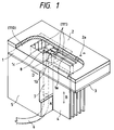
- Fig. 1 shows a first preferred embodiment of the present invention.
- reference numeral 1 designates a spacer constituting a feature of the present invention.
- the spacer is constituted by a silicon single crystal substrate of crystal orientation (110) having a thickness suitable for securing the optimum volume as a pressure generating chamber.
- through-holes 1a, 1a, 1a... to form pressure generating chambers communicating with nozzle openings 2a, 2a, 2a... of a nozzle plate 2 at one end, a through-hole 1c to form a reservoir supplied with ink from an ink tank not shown and through-holes 1b, 1b, 1b... to form ink supply ports for communicating the respective through-holes 1a, 1a, 1a... with the through-hole 1c are formed by anisotropic etching (which will be described later), and are disposed between the nozzle plate 2 and a plate member 3 (which also will be described later).
- reference numeral 2 designates the nozzle plate as described above.
- the nozzle plate is provided with the nozzle openings 2a, 2a, 2a... formed at intervals of a predetermined pitch, for example, 180 DPI, and is airtightly fixed to one surface of the spacer 1.
- Reference numeral 3 designates the plate member which is airtightly fixed to the other surface of the spacer 1 and cooperates with the nozzle plate 2 to form pressure generating chambers.
- Piezoelectric vibrators 4, 4, 4... are fixed to regions of the plate member 3 facing the pressure generating chambers.
- the piezoelectric vibrators 4, 4, 4... are formed as vertical vibration type piezoelectric vibrators which vibrate in the directions of the arrows B in the drawing, that is, in the directions perpendicular to the surface of the plate member 3. While one end of each of the piezoelectric vibrators abuts the plate member 3 as described above, the other end (the region represented by the wavy line A in the drawing) is fixed to a pedestal 5 by an adhesive agent.
- a through-hole 7 having one end communicating with an ink tank (not shown) through a tube 6 and the other, opposite end connected to an ink flow-in port 8 and to the through-hole 1c to form a reservoir as described above
- the reservoir side containing the through-holes 1b, 1b, 1b... to form ink flow passages is fixed so that a region (represented by the wave line D in the drawing) shaped like a cantilever by the through-holes 1a, 1a, 1a... and 1b, 1b, 1b... in supported without inhibition of vibration by the piezoelectric vibrators of the plate member.
- Fig. 2 is an enlarged view of the vicinity of the pressure generating chambers in the aforementioned ink-jet type recording head.
- the plate member 3 which cooperates with the through-holes 1a of the spacer 1 and the nozzle plate 2 to form pressure generating chambers has island portions 3a formed as thick portions for transmitting the expansion/-contraction of the piezoelectric vibrators 4 to the whole of the pressure generating chambers, and thin portions 3b formed to surround the island portions.
- Fig. 3(a) shows an embodiment of the aforementioned spacer.
- the spacer is applied to a recording head of the type in which the nozzle openings are arranged at intervals of a predetermined pitch, for example 141 ⁇ m, will be described as an example.
- reference numerals 1a, 1a, 1a... and 1a', 1a', 1a'... designate through-holes which form respective pressure generating chambers.
- the through-holes are arranged so as to be substantially symmetrical to each other with respect to a center line in accordance with the arrangement of nozzle trains.
- the sides facing each other of the through-holes are communicating with nozzle openings of a nozzle plate (not shown).
- through-holes 1b, 1b... and 1b', 1b'... to form ink supply ports communicating with reservoirs and through-holes 1c and 1c' to form reservoirs connected to the through-holes 1b, 1b,... and 1b', 1b'...
- each of the through-holes 1a forming pressure generating chambers as shown in Fig. 3(b) is substantially shaped like a parallelogram constituted by wall surfaces 1a-a, 1a-b, 1a-c and 1a-d perpendicular to a surface.
- one wall surface side 1a-a abutting an extension line of the wall surface 1a-d at an acute angle ⁇ in the reservoir side is provided with a through-hole 1b to form an ink supply port partitioned by a wall surface 1b-a to form the same plane as the wall surface 1a-a, so that fluid resistance suitable to jetting of ink droplets and supplying of ink to the pressure generating chamber is obtained in accordance with the width and length of the through-hole 1b.
- the wall surface 1c-a forming a through-hole 1c as a reservoir is formed to have the optimum shape as a reservoir by zigzag repetition of fine planes for correction of the orientation due to anisotropic etching.
- These through-holes 1a, 1a, 1a..., 1b, 1b, 1b... and 1c are formed as through-holes each passing through a wall from one side to the other side.
- the wall surfaces partitioning the through-holes are perpendicular to a surface of the substrate formed as spacer 1.
- Fig. 4 shows another form of arrangement of the pressure generating chambers.
- reference numeral 9 designates a silicon single crystal substrate of crystal orientation (110) having the same structure as described above. This embodiment relates to the case where the silicon single substrate is applied to a recording head having 4 nozzle opening trains.
- reference numerals 10, 10, 10... designate through-holes forming respective pressure generating chamber. These are formed as through-holes by anisotropic etching of the two sides of the silicon single crystal substrate in the same inner as described above. In one end of each of the through-holes 10, 10, 10..., that is, in a side opposite to the nozzle opening side, there are formed through-holes 11, 11, 11... to form ink supply ports.
- these through-holes 11, 11, 11... are arranged so as to be parallel to each other to form an angle of 35° with respect to an axial line of the through-holes as pressure generating chambers.
- Through-holes 12, 12, 12... as reservoirs are connected to the through-holes 11, 11, 11... as the respective groups of ink supply ports.
- ink flow-in ports 13, 13, 13... being in communication with an ink tank are connected to respective ones of the through-holes 12, 12,...
- the through-holes 10, 10, 10... forming pressure generating chambers and the through-holes 11, 11, 11... forming ink supply ports are connected to each other at an angle of about 110°, as shown in Fig. 4(b). Because they are accordingly arranged so that discontinuous portions are reduced as much as possible, points of connection between pressure generating chambers and ink supply ports are smoothed so that bubbles and the like can be prevented from stagnation.
- Fig. 6 shows the process of producing the aforementioned spacer.
- reference numeral 20 designates a silicon single crystal substrate of crystal orientation (110) having a thickness of, for example, 220 ⁇ m, necessary for functioning as a spacer.
- a silicon dioxide film 21 having a thickness of, for example, about 1 ⁇ m, necessary for functioning as a protective film in anisotropic etching is formed on the whole surface of the silicon single crystal substrate by the method of heat oxidation (Fig. 6(a)).
- Hydrogen fluoride resisting protective films 22 and 23 having windows 24 and 25 coincident with the aforementioned through-holes 1a, 1b and 1c are formed on front and rear surfaces of the substrate 20 coated with the silicon dioxide film 21 by photolithography (Fig. 6(b)).
- etching is carried out with an aqueous solution of about 17% potassium hydroxide kept at a constant temperature, for example, 80°C, in the stage in which silicon dioxide patterning is finished as described above, portions of the windows 26 and 27 are selectively subjected to etching in parallel to the plane of crystal orientation (111) from the front and rear surfaces at a speed of about 2 ⁇ m per minute with use of the silicon dioxide patterns 28 and 29 as protective films (Fig. 6(d)).
- the silicon dioxide films 28 and 29 used as masks are removed with hydrogen fluoride and then heat oxidation is carried out again to form a silicon dioxide film 31 having a sufficient thickness, for example, about 1 ⁇ m, as a protective film on the whole exposed surface.
- the silicon dioxide film 31 is used as a protective film against ink (Fig. 6(e)).
- Fig. 8 shows a producing process in the case where a silicon oxide crystalline substrate, for example, Z-cut synthetic crystal, is used as a substrate constituting a spacer.
- reference numeral 40 designates a Z-cut synthetic crystal substrate having a thickness, for example, of 220 ⁇ m, necessary for functioning as a spacer.
- a metal film 41 for example, a 50 nm (500 angstrom) chromium and 100 nm (1000 angstrom) gold film, is formed on the whole surface of the substrate by sputtering (Fig. 8(a)).
- Films 44 and 45 having windows 42 and 43 coincident with the aforementioned through-holes 1a, 1b and 1c are formed on front and rear surfaces of the substrate 40 coated with the metal protective film 41 by photolithography (Fig. 8(b)).
- the gold film and the chromium film are etched with an aqueous solution of potassium iodide and iodine and in ammoniated cerium nitrate etching solution, respectively, and then the resist film is removed with a solution of nitric acid and hydrogen peroxide (Fig. 8(c)).
- etching When etching is started from the two surfaces of the substrate with an ammonium bifluoride saturation aqueous solution or a mixture solution of hydrofluoric acid and ammonium fluoride kept at a predetermined temperature, for example, 80°C, in the stage in which a predetermined etching pattern is formed in the aforementioned manner, etching progresses at a speed of 70 ⁇ m per hour (Fig. 8(d)).
- the metal film 41 is removed with an aqueous solution of potassium iodide and iodine and an ammoniated cerium nitrate etching solution (Fig. 8(e)).
- a silicon dioxide film be formed as a protective film. It is, however, unnecessary to form a specific protective film, because the crystal has an inherent resistance to chemical corrosion.
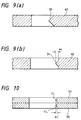
- a through-hole in which overhanging portions 54, 54 having a projecting length ⁇ L' as small as possible remain can be formed by etching a plurality of thin synthetic crystal substrates 53, 53 in the aforementioned manner, and then laminating the plurality of substrates into a predetermined thickness, as shown in Fig. 10.
- one spacer is formed by laminating a plurality of substrates, means of softening the substrates while applying pressure thereto or means of adhering the substrates by a general adhesive agent may be used.
- the spacer formed in the aforementioned manner is fixed to as to be inserted between the nozzle plate and the plate member to thereby define a flow passage constituent member.
- respective joint surfaces may be welded under pressure after applying an adhesive agent onto the respective joint surfaces. Because such assembly using an adhesive agent can be performed at ordinary temperatures with respect to the spacer, the nozzle plate and the plate member, there arises an advantage in that not only is the assembly work simple, but residual heat distortion caused by the difference between the expansion coefficients of the respective members as in the case of on alloy joining method is prevented.
- FIG. 11 shows an embodiment of a spacer improved to cope with this problem.
- reference numeral 60 designates a spacer member constituted by a silicon single crystal substrate or a synthetic crystal.
- the spacer member is formed so that chamfered portions 62a, 62a, 62a... having an angle ⁇ with respect to other surfaces of adhesion are provided in edges of partitions 62 partitioning through-holes 61 constituting pressure generating chambers and ink supply ports so as to extend in the direction of length of the partitions 62.
- the spacer 60 formed in the aforementioned manner is joined with pressure to the plate member 67 abutting the piezoelectric vibrators 66 and the nozzle plate 65 with the nozzle openings 65a after the adhesive agent 63 (Fig. 11(b)) is applied onto the surface thereof.
- an ink-jet type recording head is assembled.
- the adhesive agent 63 overflows from the gap between the spacer 60 and the nozzle plate 65 and the gap between the spacer 60 and the plate member 67 by pressure bonding after application thereof.
- the overflowing adhesive agent 63a enters into sectionally V-shaped spaces 68 formed between the chamfered portions 62a and the surface of the plate member 67 or the nozzle plate 65, is received in these spaces and spreads along the chamfered portions. Accordingly, the formation of spherical projections in specific points is prevented, as well as the change of compliance of the plate member 67, the increase of, fluid resistance of the ink supply ports to a larger value than a set value, and the reduction of the volume of each of the pressure generating chambers to a smaller value than a set value.
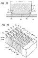
- Fig. 12 shows an embodiment in which a spacer is formed by anisotropic etching of a silicon single crystal substrate.
- isotropic etching with hydrofluoric acid is applied at the stage in which anisotropic etching is finished.
- the speed of etching of acute regions such as edge lines formed by the partitions 62 partitioning the through-holes formed by anisotropic etching and the surface becomes larger than the speed of etching of flat portions so that the edge portions are substantially selectively subjected to etching.
- each section is shaped like a circular arc, but sectionally V-shaped concave spaces are formed between the nozzle plate and the plane of the plate member so that the adhesive agent overflowing from the surfaces of adhesion can be absorbed by the spaces.
- An adhesive agent having a high viscosity such as an epoxy adhesive agent, etc ., is used for joining of these members. Because the adhesive agent is applied by a screen printing method, a pad transferring method, a roll coating method, etc ., the quantity of the adhesive agent applied can be controlled with a high accuracy. As a result, the function of the chamfered portions 62a and 62b is not affected as long as spaces capable of absorbing the adhesive agent overflowing from the surfaces of adhesion are available.
- a volume capable of absorbing the adhesive agent can be secured without reduction of the strength of the wall surfaces as long as the width ⁇ w or radius R of each of the spaces is in a range of from about 1/12 to about 1/6 the thickness of each of the partitions 62.
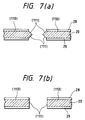
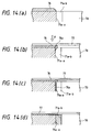
- Fig. 13 shows another embodiment of an ink-jet type recording head according to the present invention.
- reference numeral 70 designates a silicon single crystal substrate or a crystal substrate having crystal orientation (110) and having a thickness sufficient to form a spacer.
- through-holes 71, 71, 71... to form pressure generating chambers, through-holes 72, 72, 72... to form ink supply ports, and a through-hole to form a reservoir (not shown) are formed by etching.
- wall surfaces 71a , 71a of the through-holes 71, 71 to form pressure generating chambers and wall surfaces 72a, 72a of the through-holes 72, 72 to form ink supply ports are arranged sectionally rectangularly so that one surface thereof has a plurality of fine planes 71a-a, 71a-a, 71a- a... and 72a-a, 72a-a, 72a-a... and predetermined ,steps 71a-b, 71a-b, 71a-b... and 72a-b, 72a-b, 72-a-b...
- Grooves 73a and 74a extending in the direction of thickness are formed in surfaces 73, 73, 73..., 74, 74, 74, ... which do not substantially contribute to forming the aforementioned fine planes.
- an adhesive agent 76 such as an epoxy adhesive agent is applied onto surfaces of the thus-formed spacer 70 by a screen printing method, a pad transferring method, a roll coating method or the like to form a predetermined thickness (Fig. 14(a)) and then the nozzle plate or plate member 77 is pressed by a predetermined amount of pressure F, the adhesive agent surplus 76a overflows to the wall surface side of the spacer 70 (Fig. 14(b)).
- the adhesive agent spreads along the fine planes 71a-a and 72a-a due to its surface tension (Fig. 14(c)), and then the rectangular spaces constituted by the fine planes 71a-a and 72a-a and the steps 71a-b and 72a-b are filled with the adhesive agent (Fig. 14(d)).
- the adhesive agent overflowing to relatively narrow wall surfaces 73 and 74, is brought into the grooves 73a and 74a by capillary force so that the adhesive agent cannot overflow to the surface.
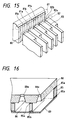
- Fig. 16 shows a further embodiment of an ink-jet type recording head according to the present invention.
- reference numeral 85 designates a silicon single crystal substrate or a synthetic crystal substrate having a thickness suitable for forming a spacer.
- Through-holes to form pressure generating chambers 86, ink supply ports and reservoirs are formed by etching.
- the surface of the spacer joined with the nozzle plate 88 having the nozzle openings 88a and the plate meter 89 by the adhesive agent is roughed by an abrasive material or grinding stone of mean particle size such that concave-convex portions 85a and 85b with surface roughnesses of the order of micrometers are formed.
- the applied adhesive agent flows into the concave-convex portions of the surfaces.
- the adhesive agent surplus tending to flow out of the regions of adhesion is kept back by the capillary force of the concave-convex portions or the rough surfaces so that the adhesive agent surplus is prevented from overflowing.
- the choking of the nozzle openings and the change of the volume of each of the pressure generating chambers and the ink supply ports is prevented.
- FIG. 17 shows a further embodiment of the present invention.
- reference numeral 90 designates a spacer constituted by a silicon single crystal substrate or a synthetic crystal substrate.
- a nozzle plate 91 having nozzle openings 91a and a plate member 92 are fixed to one surface of the spacer and the other surface of the spacer respectively by an adhesive agent.
- the spacer and pressure generating devices such as piezoelectric vibrators 93 in this embodiment are fixed to a pedestal 94 so that a pressure change is induced in the pressure generating chambers by the displacements of the piezoelectric vibrators 93 to thereby discharge ink droplets.
- through-holes 95 to form pressure generating chambers, through-holes 96 to form ink supply ports and a through-hole 97 to form a reservoir are formed by etching in the aforementioned manner.
- a plurality of partition portions 98a, 98a, 98a... for limiting fluid resistance of the ink supply ports are arranged as shown in Fig 18.
- the partition portions extend toward the through-hole 97 side, that is, toward the reservoir side, so that the length of a partition portion increases as the partition portion is arranged every four through-holes so as to be far from an ink flow-in port 99 communicating with an ink tank.
- the flow of ink from the ink supply port 99 is partly inhibited by the partition portions 98b, 98b... extending toward the reservoir so that the ink flow is converted into an ink flow toward the through-holes 96, 96, 96... to form ink supply ports in the vicinity of the partition portions.
- a part of the ink flow not inhibited by the partition portions 98b, 98b... enters the deeper side so that the other partition portions 98b, 98b... extending thereto convert the ink flow into an ink flow toward the through-holes 96, 96, 96... to form ink supply ports placed in the vicinity of the partition portions.
- an ink-jet type recording head including a nozzle plate provided with nozzle openings for jetting ink droplets; a spacer provided with partitions for partitioning pressure generating chambers, ink supply ports and reservoirs; a plate member fixed to the other surface of the spacer so as to be opposite to the nozzle plate, the nozzle plate, the spacer and the plate member being fixed to each other in a sandwich-like arrangement; and a pressure generating means for applying a change of pressure suitable for forming ink droplets to the pressure generating chambers; characterized in that the spacer is formed by etching a silicon crystalline substrate or a silicon oxide crystalline substrate from its opposite surfaces so that the pressure generating chambers, the ink supply ports and the reservoirs are formed in the form of through-holes communicating with each other; and the spacer is formed in the form of a cantilever so that the partitions for partitioning the pressure generating chambers and the ink supply ports are connected to a body on the nozzle opening
Landscapes
- Engineering & Computer Science (AREA)
- Manufacturing & Machinery (AREA)
- Particle Formation And Scattering Control In Inkjet Printers (AREA)
Applications Claiming Priority (12)
| Application Number | Priority Date | Filing Date | Title |
|---|---|---|---|
| JP31533592 | 1992-11-25 | ||
| JP315335/92 | 1992-11-25 | ||
| JP11975/93 | 1993-01-27 | ||
| JP1197593 | 1993-01-27 | ||
| JP2819193 | 1993-02-17 | ||
| JP28191/93 | 1993-02-17 | ||
| JP105578/93 | 1993-05-06 | ||
| JP10557893A JP3257140B2 (ja) | 1993-05-06 | 1993-05-06 | インクジェット記録装置 |
| JP11856193 | 1993-05-20 | ||
| JP118561/93 | 1993-05-20 | ||
| JP291187/93 | 1993-10-27 | ||
| JP29118793A JP3324621B2 (ja) | 1992-11-25 | 1993-10-27 | インクジェット式記録ヘッド |
Publications (3)
| Publication Number | Publication Date |
|---|---|
| EP0600382A2 true EP0600382A2 (fr) | 1994-06-08 |
| EP0600382A3 EP0600382A3 (en) | 1994-08-17 |
| EP0600382B1 EP0600382B1 (fr) | 1997-03-19 |
Family
ID=27548371
Family Applications (1)
| Application Number | Title | Priority Date | Filing Date |
|---|---|---|---|
| EP93119039A Expired - Lifetime EP0600382B1 (fr) | 1992-11-25 | 1993-11-25 | Tête d'impression à jet d'encre |
Country Status (4)
| Country | Link |
|---|---|
| US (2) | US5896150A (fr) |
| EP (1) | EP0600382B1 (fr) |
| DE (1) | DE69308996T2 (fr) |
| HK (1) | HK1006444A1 (fr) |
Cited By (17)
| Publication number | Priority date | Publication date | Assignee | Title |
|---|---|---|---|---|
| GB2302842A (en) * | 1995-07-03 | 1997-02-05 | Seiko Epson Corp | Nozzle plate, ink jet head and manufacturing method thereof |
| EP0694389A3 (fr) * | 1994-07-25 | 1997-03-05 | Seiko Epson Corp | Tête d'enregistrement à jet d'encre et procédé pour sa fabrication |
| EP0738599A3 (fr) * | 1995-04-19 | 1997-09-10 | Seiko Epson Corp | Tête d'enregistrement à jet d'encre et procédé pour sa fabrication |
| EP0748690A3 (fr) * | 1995-06-12 | 1998-01-28 | Seiko Epson Corporation | Tête d'impression du type à jet d'encre |
| US5723053A (en) * | 1993-11-05 | 1998-03-03 | Seiko Epson Corporation | Ink jet print head and a method of manufacturing the same |
| EP0839654A3 (fr) * | 1996-10-18 | 1998-06-10 | Seiko Epson Corporation | Tête d'impression et sa méthode de fabrication |
| EP0799700A3 (fr) * | 1996-04-05 | 1998-12-23 | Seiko Epson Corporation | Tête d'enregistrement à jet d'encre, procédé pour sa fabrication et appareil d'enregistrement à jet d'encre |
| EP0838336A3 (fr) * | 1996-10-24 | 1999-04-21 | Seiko Epson Corporation | Tête à jet d'encre et son procédé de fabrication |
| EP0875380A3 (fr) * | 1997-04-30 | 1999-10-06 | Seiko Epson Corporation | Tête d'impression à jet d'encre |
| EP0875381A3 (fr) * | 1997-04-30 | 1999-10-13 | Seiko Epson Corporation | Tête d'impression à jet d'encre |
| US5992974A (en) * | 1995-07-03 | 1999-11-30 | Seiko Epson Corporation | Ink-jet head having nozzle openings with a constant width and manufacturing method thereof |
| EP1293343A3 (fr) * | 2001-09-12 | 2003-09-24 | Canon Kabushiki Kaisha | Tête d'éjection de liquide et sa méthode de fabrication |
| EP1356939A3 (fr) * | 2002-04-25 | 2004-04-28 | Brother Kogyo Kabushiki Kaisha | Tête et imprimante jet d'encre |
| KR100474836B1 (ko) * | 2000-08-05 | 2005-03-08 | 삼성전자주식회사 | 액적 분사 장치의 제조 방법 |
| EP1642719A1 (fr) * | 2004-09-30 | 2006-04-05 | Brother Kogyo Kabushiki Kaisha | Tête jet d'encre |
| CN103072377A (zh) * | 2011-09-16 | 2013-05-01 | 株式会社理光 | 液体排出头以及图像形成装置 |
| CN115720551A (zh) * | 2020-06-24 | 2023-02-28 | 柯尼卡美能达株式会社 | 图像形成装置 |
Families Citing this family (22)
| Publication number | Priority date | Publication date | Assignee | Title |
|---|---|---|---|---|
| US6371598B1 (en) | 1994-04-20 | 2002-04-16 | Seiko Epson Corporation | Ink jet recording apparatus, and an ink jet head |
| US7003857B1 (en) | 1995-11-24 | 2006-02-28 | Seiko Epson Corporation | Method of producing an ink-jet printing head |
| JP3460218B2 (ja) * | 1995-11-24 | 2003-10-27 | セイコーエプソン株式会社 | インクジェットプリンタヘッドおよびその製造方法 |
| US6433471B1 (en) * | 1996-01-19 | 2002-08-13 | Philips Electronics North America Corporation | Plasma addressed liquid crystal display with glass spacers |
| US6334672B1 (en) * | 1996-04-18 | 2002-01-01 | Minolta Co., Ltd. | Inkjet recording head having a driving source attached by a chamfered adhesive layer |
| JPH10264374A (ja) * | 1997-03-27 | 1998-10-06 | Seiko Epson Corp | インクジェット式記録ヘッド |
| JP3887137B2 (ja) * | 1999-01-29 | 2007-02-28 | セイコーインスツル株式会社 | 圧電振動子の製造方法 |
| US6303042B1 (en) * | 1999-03-02 | 2001-10-16 | Eastman Kodak Company | Making ink jet nozzle plates |
| US6258286B1 (en) * | 1999-03-02 | 2001-07-10 | Eastman Kodak Company | Making ink jet nozzle plates using bore liners |
| US6631980B2 (en) | 2000-01-19 | 2003-10-14 | Seiko Epson Corporation | Liquid jetting head |
| US20020134749A1 (en) * | 2001-01-26 | 2002-09-26 | Chromux Technologies. Inc. | Method of making a vertical, mirror quality surface in silicon and mirror made by the method |
| CN1549962A (zh) * | 2001-08-30 | 2004-11-24 | �ձ�д��ӡˢ��ʽ���� | 可再剥离透明触摸板安装结构及其中所用的安装用片 |
| JP2004312666A (ja) * | 2003-03-25 | 2004-11-04 | Fuji Photo Film Co Ltd | 固体撮像装置及び固体撮像装置の製造方法 |
| JP4228239B2 (ja) | 2006-09-13 | 2009-02-25 | セイコーエプソン株式会社 | 液体噴射ヘッド及び液体噴射装置 |
| JP4911189B2 (ja) * | 2009-03-30 | 2012-04-04 | ブラザー工業株式会社 | 液体吐出装置およびその製造方法 |
| JP5914969B2 (ja) | 2011-01-13 | 2016-05-11 | セイコーエプソン株式会社 | 液体噴射ヘッド及び液体噴射装置 |
| KR101846400B1 (ko) * | 2011-12-31 | 2018-04-09 | 삼성전자주식회사 | 잉크젯 프린트 헤드 및 그 제조방법 |
| JP6569088B2 (ja) * | 2014-06-27 | 2019-09-04 | パナソニックIpマネジメント株式会社 | インクジェットヘッドとそれを用いた塗布装置 |
| JP2017080946A (ja) * | 2015-10-26 | 2017-05-18 | セイコーエプソン株式会社 | Memsデバイスの製造方法、memsデバイス、液体噴射ヘッド、および液体噴射装置 |
| WO2017150085A1 (fr) * | 2016-03-03 | 2017-09-08 | 株式会社リコー | Tête de décharge de liquide, unité de décharge de liquide, et dispositif servant à décharger un liquide |
| JP7087521B2 (ja) * | 2018-03-22 | 2022-06-21 | ブラザー工業株式会社 | 液体吐出ヘッド及び液体吐出ヘッドの製造方法 |
| CN111204136A (zh) * | 2018-11-22 | 2020-05-29 | 东芝泰格有限公司 | 液体喷出头及流路部件 |
Family Cites Families (16)
| Publication number | Priority date | Publication date | Assignee | Title |
|---|---|---|---|---|
| US4047184A (en) * | 1976-01-28 | 1977-09-06 | International Business Machines Corporation | Charge electrode array and combination for ink jet printing and method of manufacture |
| US4216483A (en) * | 1977-11-16 | 1980-08-05 | Silonics, Inc. | Linear array ink jet assembly |
| JPS5840512B2 (ja) * | 1978-10-04 | 1983-09-06 | 株式会社リコー | インクジェット記録装置 |
| JPS5586767A (en) * | 1978-12-23 | 1980-06-30 | Seiko Epson Corp | Print head |
| JPS5644671A (en) * | 1979-09-21 | 1981-04-23 | Seiko Epson Corp | Ink-jet head |
| US4312008A (en) * | 1979-11-02 | 1982-01-19 | Dataproducts Corporation | Impulse jet head using etched silicon |
| JPS57201665A (en) * | 1981-06-05 | 1982-12-10 | Hitachi Ltd | Ink jet device |
| JPS5869068A (ja) * | 1981-10-20 | 1983-04-25 | Ricoh Co Ltd | インクジエツト記録装置 |
| US4611219A (en) * | 1981-12-29 | 1986-09-09 | Canon Kabushiki Kaisha | Liquid-jetting head |
| JPS58220756A (ja) * | 1982-06-18 | 1983-12-22 | Canon Inc | インクジエツト記録ヘツドの製造方法 |
| US4516140A (en) * | 1983-12-27 | 1985-05-07 | At&T Teletype Corporation | Print head actuator for an ink jet printer |
| US4786357A (en) * | 1987-11-27 | 1988-11-22 | Xerox Corporation | Thermal ink jet printhead and fabrication method therefor |
| US4829324A (en) * | 1987-12-23 | 1989-05-09 | Xerox Corporation | Large array thermal ink jet printhead |
| US5157420A (en) * | 1989-08-17 | 1992-10-20 | Takahiro Naka | Ink jet recording head having reduced manufacturing steps |
| DE3938282A1 (de) * | 1989-11-17 | 1991-05-23 | Bayer Ag | Verfahren zur herstellung von 3,8-dihydroxy-5a,10b-diphenylcumarano-2',3',2,3-cumaran |
| US5265315A (en) * | 1990-11-20 | 1993-11-30 | Spectra, Inc. | Method of making a thin-film transducer ink jet head |
-
1993
- 1993-11-24 US US08/156,909 patent/US5896150A/en not_active Expired - Fee Related
- 1993-11-25 EP EP93119039A patent/EP0600382B1/fr not_active Expired - Lifetime
- 1993-11-25 DE DE69308996T patent/DE69308996T2/de not_active Expired - Fee Related
-
1998
- 1998-06-19 HK HK98105738A patent/HK1006444A1/en not_active IP Right Cessation
-
1999
- 1999-01-22 US US09/235,401 patent/US6309057B1/en not_active Expired - Fee Related
Cited By (39)
| Publication number | Priority date | Publication date | Assignee | Title |
|---|---|---|---|---|
| EP0980757A3 (fr) * | 1993-11-05 | 2000-12-06 | Seiko Epson Corporation | Tête d'impression par jet d'encre |
| US5956058A (en) * | 1993-11-05 | 1999-09-21 | Seiko Epson Corporation | Ink jet print head with improved spacer made from silicon single-crystal substrate |
| EP0980759A3 (fr) * | 1993-11-05 | 2000-12-06 | Seiko Epson Corporation | Tête d'impression par jet d'encre et sa méthode de fabrication |
| US5723053A (en) * | 1993-11-05 | 1998-03-03 | Seiko Epson Corporation | Ink jet print head and a method of manufacturing the same |
| EP0652108A3 (fr) * | 1993-11-05 | 1998-04-01 | Seiko Epson Corporation | Tête d'impression par jet d'encre et sa méthode de fabrication |
| EP0980756A3 (fr) * | 1993-11-05 | 2000-12-06 | Seiko Epson Corporation | Tête d'impression par jet d'encre |
| EP0980755A3 (fr) * | 1993-11-05 | 2000-12-06 | Seiko Epson Corporation | Tête d'impression par jet d'encre et sa méthode de fabrication |
| EP0694389A3 (fr) * | 1994-07-25 | 1997-03-05 | Seiko Epson Corp | Tête d'enregistrement à jet d'encre et procédé pour sa fabrication |
| US6048053A (en) * | 1994-07-25 | 2000-04-11 | Seiko Epson Corporation | Ink jet recording head including a spacing member for defining a gap between a fixed board and a piezoelectric element |
| US5754205A (en) * | 1995-04-19 | 1998-05-19 | Seiko Epson Corporation | Ink jet recording head with pressure chambers arranged along a 112 lattice orientation in a single-crystal silicon substrate |
| EP0738599A3 (fr) * | 1995-04-19 | 1997-09-10 | Seiko Epson Corp | Tête d'enregistrement à jet d'encre et procédé pour sa fabrication |
| US5896149A (en) * | 1995-06-12 | 1999-04-20 | Seiko Epson Corporation | Ink jet type recording head having a flow passage substrate with a stepped configuration and recesses formed in a surface thereof |
| EP0748690A3 (fr) * | 1995-06-12 | 1998-01-28 | Seiko Epson Corporation | Tête d'impression du type à jet d'encre |
| GB2302842B (en) * | 1995-07-03 | 1998-12-30 | Seiko Epson Corp | A nozzle plate, ink-jet head and manufacturing method thereof |
| GB2302842A (en) * | 1995-07-03 | 1997-02-05 | Seiko Epson Corp | Nozzle plate, ink jet head and manufacturing method thereof |
| US5992974A (en) * | 1995-07-03 | 1999-11-30 | Seiko Epson Corporation | Ink-jet head having nozzle openings with a constant width and manufacturing method thereof |
| US6238585B1 (en) * | 1995-07-03 | 2001-05-29 | Seiko Epson Corporation | Method for manufacturing an ink-jet head having nozzle openings with a constant width |
| US6137511A (en) * | 1996-04-05 | 2000-10-24 | Seiko Epson Corporation | Ink jet recording head having an ink reservoir comprising a plurality of grooves with increased strength and volume capacity and ink jet recording apparatus having the same |
| EP0799700A3 (fr) * | 1996-04-05 | 1998-12-23 | Seiko Epson Corporation | Tête d'enregistrement à jet d'encre, procédé pour sa fabrication et appareil d'enregistrement à jet d'encre |
| US6290341B1 (en) | 1996-10-18 | 2001-09-18 | Seiko Epson Corporation | Ink jet printing head which prevents the stagnation of ink in the vicinity of the nozzle orifices |
| US6789319B2 (en) | 1996-10-18 | 2004-09-14 | Seiko Epson Corporation | Method of manufacturing an ink jet print head |
| EP0839654A3 (fr) * | 1996-10-18 | 1998-06-10 | Seiko Epson Corporation | Tête d'impression et sa méthode de fabrication |
| EP1108545A1 (fr) * | 1996-10-18 | 2001-06-20 | Seiko Epson Corporation | Tête d'impression et sa méthode de fabrication |
| US7153442B2 (en) | 1996-10-18 | 2006-12-26 | Seiko Epson Corporation | Method of manufacturing an ink jet print head |
| US6260960B1 (en) | 1996-10-24 | 2001-07-17 | Seiko Epson Corporation | Ink jet print head formed through anisotropic wet and dry etching |
| EP0838336A3 (fr) * | 1996-10-24 | 1999-04-21 | Seiko Epson Corporation | Tête à jet d'encre et son procédé de fabrication |
| US6231169B1 (en) | 1997-04-30 | 2001-05-15 | Seiko Epson Corporation | Ink jet printing head including a backing member for reducing displacement of partitions between pressure generating chambers |
| EP0875380A3 (fr) * | 1997-04-30 | 1999-10-06 | Seiko Epson Corporation | Tête d'impression à jet d'encre |
| EP0875381A3 (fr) * | 1997-04-30 | 1999-10-13 | Seiko Epson Corporation | Tête d'impression à jet d'encre |
| US6332672B1 (en) | 1997-04-30 | 2001-12-25 | Seiko Epson Corporation | Ink jet recording head including a cap member sealing piezoelectric vibrators |
| KR100474836B1 (ko) * | 2000-08-05 | 2005-03-08 | 삼성전자주식회사 | 액적 분사 장치의 제조 방법 |
| US6799831B2 (en) | 2001-09-12 | 2004-10-05 | Canon Kabushiki Kaisha | Liquid discharge recording head and method for manufacturing the same |
| EP1293343A3 (fr) * | 2001-09-12 | 2003-09-24 | Canon Kabushiki Kaisha | Tête d'éjection de liquide et sa méthode de fabrication |
| EP1356939A3 (fr) * | 2002-04-25 | 2004-04-28 | Brother Kogyo Kabushiki Kaisha | Tête et imprimante jet d'encre |
| US6926382B2 (en) | 2002-04-25 | 2005-08-09 | Brother Kogyo Kabushiki Kaisha | Ink-jet head and ink-jet printer |
| EP1642719A1 (fr) * | 2004-09-30 | 2006-04-05 | Brother Kogyo Kabushiki Kaisha | Tête jet d'encre |
| CN103072377A (zh) * | 2011-09-16 | 2013-05-01 | 株式会社理光 | 液体排出头以及图像形成装置 |
| CN103072377B (zh) * | 2011-09-16 | 2015-11-18 | 株式会社理光 | 液体排出头以及图像形成装置 |
| CN115720551A (zh) * | 2020-06-24 | 2023-02-28 | 柯尼卡美能达株式会社 | 图像形成装置 |
Also Published As
| Publication number | Publication date |
|---|---|
| US6309057B1 (en) | 2001-10-30 |
| EP0600382A3 (en) | 1994-08-17 |
| DE69308996T2 (de) | 1997-10-23 |
| DE69308996D1 (de) | 1997-04-24 |
| US5896150A (en) | 1999-04-20 |
| HK1006444A1 (en) | 1999-02-26 |
| EP0600382B1 (fr) | 1997-03-19 |
Similar Documents
| Publication | Publication Date | Title |
|---|---|---|
| EP0600382B1 (fr) | Tête d'impression à jet d'encre | |
| HK1006444B (en) | Ink-jet type recording head | |
| US4639748A (en) | Ink jet printhead with integral ink filter | |
| US4216477A (en) | Nozzle head of an ink-jet printing apparatus with built-in fluid diodes | |
| US5041190A (en) | Method of fabricating channel plates and ink jet printheads containing channel plates | |
| GB2182611A (en) | Impulse ink jet print head and methods of making the same | |
| EP0565280B1 (fr) | Méthode de fabrication d'une tête d'impression utilisant un élément piézo-électrique | |
| EP0967080B1 (fr) | Tête d'impression à jet d' encre et procédé de fabrication | |
| JPH0655733A (ja) | インクジェットヘッド及びその製造方法 | |
| JP3324621B2 (ja) | インクジェット式記録ヘッド | |
| EP0839654B1 (fr) | Tête d'impression et sa méthode de fabrication | |
| JPH05229128A (ja) | インクジェット印字ヘッドの製造方法 | |
| JPH07178909A (ja) | インクジェット式記録ヘッド | |
| US6332667B1 (en) | Orifice member of nozzle for ink-jet printing | |
| JPH06206315A (ja) | インクジェットヘッドの製造方法 | |
| EP0757940B1 (fr) | Tête d'enregistrement à jet de liquide et son procédé de fabrication ainsi qu'un appareil d'enregistrement à jet de liquide dans lequel est montée ladite tête d'enregistrement à jet de liquide | |
| US6958125B2 (en) | Method for manufacturing liquid jet recording head | |
| JP4033371B2 (ja) | インクジェットヘッド及びその製造方法、画像形成装置 | |
| JP2861117B2 (ja) | インクジェットプリンタヘッド及びその製造方法 | |
| JP3324622B2 (ja) | シリコン単結晶基板のエッチング加工方法 | |
| JPH0331584B2 (fr) | ||
| JP2002326360A (ja) | 液体吐出ヘッドの製造方法 | |
| JPS61163863A (ja) | インクジエツトプリンタ用ヘツドの製造方法 | |
| JPH04191054A (ja) | インクジェット記録ヘッド及びその製造方法 | |
| JPH0323346B2 (fr) |
Legal Events
| Date | Code | Title | Description |
|---|---|---|---|
| PUAI | Public reference made under article 153(3) epc to a published international application that has entered the european phase |
Free format text: ORIGINAL CODE: 0009012 |
|
| AK | Designated contracting states |
Kind code of ref document: A2 Designated state(s): CH DE FR GB IT LI NL SE |
|
| PUAL | Search report despatched |
Free format text: ORIGINAL CODE: 0009013 |
|
| AK | Designated contracting states |
Kind code of ref document: A3 Designated state(s): CH DE FR GB IT LI NL SE |
|
| 17P | Request for examination filed |
Effective date: 19941013 |
|
| 17Q | First examination report despatched |
Effective date: 19951116 |
|
| GRAG | Despatch of communication of intention to grant |
Free format text: ORIGINAL CODE: EPIDOS AGRA |
|
| GRAH | Despatch of communication of intention to grant a patent |
Free format text: ORIGINAL CODE: EPIDOS IGRA |
|
| GRAH | Despatch of communication of intention to grant a patent |
Free format text: ORIGINAL CODE: EPIDOS IGRA |
|
| GRAA | (expected) grant |
Free format text: ORIGINAL CODE: 0009210 |
|
| AK | Designated contracting states |
Kind code of ref document: B1 Designated state(s): CH DE FR GB IT LI NL SE |
|
| REG | Reference to a national code |
Ref country code: CH Ref legal event code: EP |
|
| ITF | It: translation for a ep patent filed | ||
| REF | Corresponds to: |
Ref document number: 69308996 Country of ref document: DE Date of ref document: 19970424 |
|
| ET | Fr: translation filed | ||
| REG | Reference to a national code |
Ref country code: CH Ref legal event code: NV Representative=s name: BOVARD AG PATENTANWAELTE |
|
| PLBE | No opposition filed within time limit |
Free format text: ORIGINAL CODE: 0009261 |
|
| STAA | Information on the status of an ep patent application or granted ep patent |
Free format text: STATUS: NO OPPOSITION FILED WITHIN TIME LIMIT |
|
| 26N | No opposition filed | ||
| REG | Reference to a national code |
Ref country code: GB Ref legal event code: IF02 |
|
| PGFP | Annual fee paid to national office [announced via postgrant information from national office to epo] |
Ref country code: NL Payment date: 20071115 Year of fee payment: 15 Ref country code: DE Payment date: 20071122 Year of fee payment: 15 |
|
| PGFP | Annual fee paid to national office [announced via postgrant information from national office to epo] |
Ref country code: IT Payment date: 20071127 Year of fee payment: 15 Ref country code: CH Payment date: 20071128 Year of fee payment: 15 |
|
| PGFP | Annual fee paid to national office [announced via postgrant information from national office to epo] |
Ref country code: SE Payment date: 20071106 Year of fee payment: 15 |
|
| PGFP | Annual fee paid to national office [announced via postgrant information from national office to epo] |
Ref country code: GB Payment date: 20071121 Year of fee payment: 15 Ref country code: FR Payment date: 20071108 Year of fee payment: 15 |
|
| REG | Reference to a national code |
Ref country code: CH Ref legal event code: PL |
|
| EUG | Se: european patent has lapsed | ||
| GBPC | Gb: european patent ceased through non-payment of renewal fee |
Effective date: 20081125 |
|
| PG25 | Lapsed in a contracting state [announced via postgrant information from national office to epo] |
Ref country code: NL Free format text: LAPSE BECAUSE OF NON-PAYMENT OF DUE FEES Effective date: 20090601 |
|
| NLV4 | Nl: lapsed or anulled due to non-payment of the annual fee |
Effective date: 20090601 |
|
| PG25 | Lapsed in a contracting state [announced via postgrant information from national office to epo] |
Ref country code: IT Free format text: LAPSE BECAUSE OF NON-PAYMENT OF DUE FEES Effective date: 20081125 |
|
| REG | Reference to a national code |
Ref country code: FR Ref legal event code: ST Effective date: 20090731 |
|
| PG25 | Lapsed in a contracting state [announced via postgrant information from national office to epo] |
Ref country code: LI Free format text: LAPSE BECAUSE OF NON-PAYMENT OF DUE FEES Effective date: 20081130 Ref country code: DE Free format text: LAPSE BECAUSE OF NON-PAYMENT OF DUE FEES Effective date: 20090603 Ref country code: CH Free format text: LAPSE BECAUSE OF NON-PAYMENT OF DUE FEES Effective date: 20081130 |
|
| PG25 | Lapsed in a contracting state [announced via postgrant information from national office to epo] |
Ref country code: GB Free format text: LAPSE BECAUSE OF NON-PAYMENT OF DUE FEES Effective date: 20081125 |
|
| PG25 | Lapsed in a contracting state [announced via postgrant information from national office to epo] |
Ref country code: SE Free format text: LAPSE BECAUSE OF NON-PAYMENT OF DUE FEES Effective date: 20081126 |
|
| PG25 | Lapsed in a contracting state [announced via postgrant information from national office to epo] |
Ref country code: FR Free format text: LAPSE BECAUSE OF NON-PAYMENT OF DUE FEES Effective date: 20081130 |