EP0600499B1 - Steuerschaltung für Flüssigkristallanzeigevorrichtung - Google Patents
Steuerschaltung für Flüssigkristallanzeigevorrichtung Download PDFInfo
- Publication number
- EP0600499B1 EP0600499B1 EP93119471A EP93119471A EP0600499B1 EP 0600499 B1 EP0600499 B1 EP 0600499B1 EP 93119471 A EP93119471 A EP 93119471A EP 93119471 A EP93119471 A EP 93119471A EP 0600499 B1 EP0600499 B1 EP 0600499B1
- Authority
- EP
- European Patent Office
- Prior art keywords
- liquid crystal
- switching means
- output
- period
- driving circuit
- Prior art date
- Legal status (The legal status is an assumption and is not a legal conclusion. Google has not performed a legal analysis and makes no representation as to the accuracy of the status listed.)
- Expired - Lifetime
Links
- 239000004973 liquid crystal related substance Substances 0.000 title claims description 60
- 238000010586 diagram Methods 0.000 description 14
- 230000004044 response Effects 0.000 description 8
- 239000000758 substrate Substances 0.000 description 4
- XUIMIQQOPSSXEZ-UHFFFAOYSA-N Silicon Chemical compound [Si] XUIMIQQOPSSXEZ-UHFFFAOYSA-N 0.000 description 3
- 230000000694 effects Effects 0.000 description 3
- 229910052710 silicon Inorganic materials 0.000 description 3
- 239000010703 silicon Substances 0.000 description 3
- 230000008859 change Effects 0.000 description 2
- 239000004020 conductor Substances 0.000 description 2
- 238000010276 construction Methods 0.000 description 2
- 238000004519 manufacturing process Methods 0.000 description 2
- 239000011159 matrix material Substances 0.000 description 2
- 230000004048 modification Effects 0.000 description 2
- 238000012986 modification Methods 0.000 description 2
- 230000009471 action Effects 0.000 description 1
- 230000003213 activating effect Effects 0.000 description 1
- 230000007547 defect Effects 0.000 description 1
- 230000001419 dependent effect Effects 0.000 description 1
- 239000004065 semiconductor Substances 0.000 description 1
- 239000010409 thin film Substances 0.000 description 1
Images


Classifications
-
- G—PHYSICS
- G09—EDUCATION; CRYPTOGRAPHY; DISPLAY; ADVERTISING; SEALS
- G09G—ARRANGEMENTS OR CIRCUITS FOR CONTROL OF INDICATING DEVICES USING STATIC MEANS TO PRESENT VARIABLE INFORMATION
- G09G3/00—Control arrangements or circuits, of interest only in connection with visual indicators other than cathode-ray tubes
- G09G3/20—Control arrangements or circuits, of interest only in connection with visual indicators other than cathode-ray tubes for presentation of an assembly of a number of characters, e.g. a page, by composing the assembly by combination of individual elements arranged in a matrix no fixed position being assigned to or needed to be assigned to the individual characters or partial characters
- G09G3/34—Control arrangements or circuits, of interest only in connection with visual indicators other than cathode-ray tubes for presentation of an assembly of a number of characters, e.g. a page, by composing the assembly by combination of individual elements arranged in a matrix no fixed position being assigned to or needed to be assigned to the individual characters or partial characters by control of light from an independent source
- G09G3/36—Control arrangements or circuits, of interest only in connection with visual indicators other than cathode-ray tubes for presentation of an assembly of a number of characters, e.g. a page, by composing the assembly by combination of individual elements arranged in a matrix no fixed position being assigned to or needed to be assigned to the individual characters or partial characters by control of light from an independent source using liquid crystals
- G09G3/3611—Control of matrices with row and column drivers
- G09G3/3685—Details of drivers for data electrodes
- G09G3/3688—Details of drivers for data electrodes suitable for active matrices only
-
- G—PHYSICS
- G09—EDUCATION; CRYPTOGRAPHY; DISPLAY; ADVERTISING; SEALS
- G09G—ARRANGEMENTS OR CIRCUITS FOR CONTROL OF INDICATING DEVICES USING STATIC MEANS TO PRESENT VARIABLE INFORMATION
- G09G3/00—Control arrangements or circuits, of interest only in connection with visual indicators other than cathode-ray tubes
- G09G3/20—Control arrangements or circuits, of interest only in connection with visual indicators other than cathode-ray tubes for presentation of an assembly of a number of characters, e.g. a page, by composing the assembly by combination of individual elements arranged in a matrix no fixed position being assigned to or needed to be assigned to the individual characters or partial characters
- G09G3/2007—Display of intermediate tones
- G09G3/2011—Display of intermediate tones by amplitude modulation
-
- G—PHYSICS
- G09—EDUCATION; CRYPTOGRAPHY; DISPLAY; ADVERTISING; SEALS
- G09G—ARRANGEMENTS OR CIRCUITS FOR CONTROL OF INDICATING DEVICES USING STATIC MEANS TO PRESENT VARIABLE INFORMATION
- G09G2230/00—Details of flat display driving waveforms
-
- G—PHYSICS
- G09—EDUCATION; CRYPTOGRAPHY; DISPLAY; ADVERTISING; SEALS
- G09G—ARRANGEMENTS OR CIRCUITS FOR CONTROL OF INDICATING DEVICES USING STATIC MEANS TO PRESENT VARIABLE INFORMATION
- G09G2310/00—Command of the display device
- G09G2310/02—Addressing, scanning or driving the display screen or processing steps related thereto
- G09G2310/0264—Details of driving circuits
- G09G2310/027—Details of drivers for data electrodes, the drivers handling digital grey scale data, e.g. use of D/A converters
-
- G—PHYSICS
- G09—EDUCATION; CRYPTOGRAPHY; DISPLAY; ADVERTISING; SEALS
- G09G—ARRANGEMENTS OR CIRCUITS FOR CONTROL OF INDICATING DEVICES USING STATIC MEANS TO PRESENT VARIABLE INFORMATION
- G09G2310/00—Command of the display device
- G09G2310/02—Addressing, scanning or driving the display screen or processing steps related thereto
- G09G2310/0264—Details of driving circuits
- G09G2310/0286—Details of a shift registers arranged for use in a driving circuit
-
- G—PHYSICS
- G09—EDUCATION; CRYPTOGRAPHY; DISPLAY; ADVERTISING; SEALS
- G09G—ARRANGEMENTS OR CIRCUITS FOR CONTROL OF INDICATING DEVICES USING STATIC MEANS TO PRESENT VARIABLE INFORMATION
- G09G2330/00—Aspects of power supply; Aspects of display protection and defect management
- G09G2330/02—Details of power systems and of start or stop of display operation
- G09G2330/021—Power management, e.g. power saving
Definitions
- the present invention relates to a liquid crystal device driving circuit, and more specifically, to a circuit for driving a liquid crystal display panel capable of displaying an image with a multiple tone level.
- a liquid crystal device driving circuit for generating a source voltage driving a liquid crystal display panel typified by an active matrix type
- a circuit for enabling a multiple tone or gray scale image on the order of eight gray scale levels has been implemented in the form of a LSI (large scale integrated circuit) and is now under mass production and widely used.
- Figure 1 is a block diagram showing one example of a conventional liquid crystal device driving circuit.
- a drive voltage corresponding to a required luminance is required to supply a drive voltage corresponding to a required luminance, from drive voltage output terminals T1 to Tk of a transistor switch circuit 3 to corresponding source lines of the liquid crystal display panel.
- the drive circuit includes "k" stages of "n"-bit shift registers 15a to 15k receiving an image input data Vi from an image data input terminal, a corresponding number of "n"-bit latches 16a to 16k each for latching the "n”-bit data of a corresponding one of the "n”-bit shift registers 15a to 15k, and a corresponding number of selector circuits 14a to 14k for selectively turning on output transistors Q11 to Qmk included in the transistor switch circuit 3 on the basis of an output of the latches 16a to 16k.
- an "n"-bit digital image input data Vi indicative of "m” gray scale levels is supplied from the image data input terminal 7, and shifted and stored in the "n"-bit shift registers 15a to 15k in response to a clock pulse Vc applied to a clock input terminal 1.
- a latch pulse Vr applied to a latch pulse input terminal 2 the data stored in each of the registers is transferred to a corresponding one of the "n"-bit latches 16a to 16k.
- the "n"-bit data latched in each latch is decoded by a corresponding one of the selector circuits 14a to 14k to the effect that one transistor of the first "m” output stage transistors Q11 to Qm1 connected to the drive output terminal T1 of the transistor switch circuit 3 is turned on, and one transistor of the "k"th "m” output stage transistors Q1k to Qmk connected to the drive output terminal Tk is turned on.
- voltages V1, V2, ⁇ ⁇ ⁇ , V m corresponding to drain voltage terminals 8a to 8m of "m” gray scale levels are supplied, so that voltages of "m” gray scale levels are supplied to an external liquid crystal display.
- the voltage Vo appearing on the drive output terminal T1 is as shown in Figure 2.
- Figure 3 is a block diagram of this liquid crystal display driving circuit, and in Figure 3, the elements similar to those shown in Figure 1 are given the same Reference Numerals.
- the drive circuit includes "k" stages of "(n+1)"-bit shift registers 5a to 5k receiving an image input data from an image data input terminal 7, a corresponding number of "(n+1)"-bit latches 6a to 6k each for latching the "(n+1)"-bit data of a corresponding one of the "(n+1)”-bit shift registers 5a to 5k, and a corresponding number of selector circuits 4a to 4k for selectively turning on output transistors Q11 to Qmk included in the transistor switch circuit 3 by decoding the data outputted from the latches 6a to 6k.
- a drive output voltage Vo is generated on each of the drive voltage output terminals T 1 to T k .
- a digital image input data Vi formed of "(n+1)" bits (D 0 , D 1 , ⁇ ⁇ ⁇ , D n ) is supplied from the input terminal 7, and sequentially shifted and stored in the "(n+1)"-bit shift registers 5a to 5k in response to a clock pulse Vc.
- a latch pulse Vr the data stored in each of the registers is transferred to a corresponding one of the "(n+1)"-bit latches 6a to 6k.
- the "(n+1 )"-bit data latched in each latch is decoded by a corresponding one of the selector circuits 4a to 4k to the effect that either one transistor or two transistors of the first "m” output stage transistors Q11 to Qm1 connected to the drive output terminal T1 of the transistor switch circuit 3 is simultaneously turned on, and either one transistor or two transistors of the "k"th "m” output stage transistors Q1k to Qmk connected to the drive output terminal Tk is simultaneously turned on.
- voltages V1, V2, ⁇ ⁇ ⁇ , V m corresponding to drain voltage terminals 8a to 8m of "m” gray scale levels or their combined voltages are generated.
- the output transistors are equally formed on the same silicon substrate, the characteristics of the output transistors Q 11 to Q mk have only a little variation in a relative small zone within the same chip, even if it greatly varies from one manufacturing lot to another and from one wafer to another. Namely, the variation of the transistors is on the order of 10% at maximum. Therefore, it becomes Vo ⁇ (V 1 +V 2 )/2, depending on a ratio in on-resistance ratio of the output transistors Q 11 and Q 21 . Furthermore, in order to realize a multiple gray scale level in the liquid crystal display panel, the intervals of voltage steps are obtained by dividing the voltage of about 3 V to 4 V applied to the liquid crystal display, by the number of required gray scale levels.
- the switching elements of the transistor switch circuit 3 have been composed of the transistors Q 11 to Q mk .
- the transistors are replaced with transfer gates, the same effect can be obtained.
- the conventional liquid crystal device driving circuit can realize the (2m - 1) gray scale levels, by simultaneously turning on any two transistors of each "m" transistors of the output transistors Q 1k to Q mk by action of the selector circuit 4k.
- the potential difference between the simultaneously turned-on transistors is large, a very large current is required for the conventional liquid crystal device driving circuit, and therefore, the consumed electric power correspondingly becomes large. This is not practical.
- EP-A-0,478,386 discloses a drive circuit for a display apparatus.
- a plurality of parallel signal electrodes are provided, one of a plurality of signal voltages having different levels is output in accordance with a digital video signal being input, or two adjacent ones of said signal voltages are simultaneously output.
- one of the signal voltages is supplied to a signal electrode in one portion of one output period, and another of the signal voltages is supplied to the signal electrode in another portion of the output period.
- Another object of the present invention is to provide a driving circuit for a multiple gray scale liquid crystal device, with a reduced number of external voltage supplies and with a reduced consumed electric power.
- a liquid crystal display driving circuit according to the present invention is defined in claim 1.
- Dependent claims 2 to 6 disclose particular embodiments of the invention.
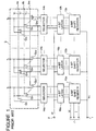
- FIG. 5 there is shown a block diagram of one embodiment of the liquid crystal device driving circuit in accordance with the present invention.
- the most significant bit of the 5-bit image data is labelled “D M3 "
- the least significant bit of the 8-bit image data is labelled "D H0 ".
- the bits “D M3 " to "D M0 " of the 5-bit image data are called “main bits”
- the bit "D H0 " of the 5-bit image data is called a "sub (interpolating) bit”.
- the shown drive circuit includes "k" stages of 5-bit shift registers 20a to 20k receiving an image input data from an image data input terminal 7, a corresponding number of 5-bit latches 21a to 21k each for latching the 5-bit data of a corresponding one of the 5-bit shift registers 20a to 20k, external gray scale level voltages V R0 , V R1 , ⁇ ⁇ ⁇ , V R16 corresponding to 16 gray scale levels, a corresponding number of output circuits 22a to 22k each generating an intermediate voltage between each pair of adjacent voltages of the gray scale level voltages V R0 , V R1 , ⁇ ⁇ ⁇ , V R16 on the basis of the interpolating bit "D H0 ", and a corresponding number of AND gates ANDa to ANDk for controlling the output of the interpolating bit "D H0 " from the 5-bit latches 21a to 21k to the output circuits 22a to 22k on the basis of an output voltage interpolating input Vh.
- FIG. 6 shows a circuit diagram of the output circuits 22a to 22k.
- Each of the output circuits 22a to 22k includes a decoder 24 receiving the main bits "D M3 " to "D M0 " of 4 bits for activating one selection signal, transfer gates TG 0 to TG 16 connected to the external gray scale level voltages V R0 , v R1 , ⁇ , V R16 , respectively, and control circuits SE 0 to SE 16 each receiving the interpolating bit "D H0 " and a corresponding one of outputs O M0 to O M16 of the decoder 24 for controlling a corresponding one of the transfer gates.
- Each of the control circuits SE 0 to SE 16 is formed of one AND gate and one OR gate connected as shown.
- the 5-bit image input data D M3 to D M0 and D H0 is supplied through the image input terminal 7, and transferred through the 5-bit shift registers 20a to 20k in response to the clock pulse Vc.
- the image input data in the 5-bit shift registers 20a to 20k is transferred and latched in the 5-bit latches 21a to 21k.
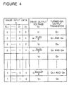
- the main bits D M3 to D M0 of the data latched in each latch are supplied to the decoder 24 of a corresponding output circuit 22a to 22k, so that an active selection pulse is outputted from one of the outputs O M0 to O M16 of the decoder in accordance with the content of the main bits D M3 to D M0 , as shown in Figure 7.
- the label "ON" shows an active condition
- the label "OFF" indicates an inactive condition.
- the sub bit D H0 of the data latched in each latch is supplied through the AND gates ANDa to ANDk to the control circuits SE 0 to SE 16 of each output circuit 22a to 22k when the output voltage interpolating input Vh is "1" (high level).
- the control circuits SE 0 to SE 16 output the signals received from the outputs O M0 to O M16 of the decoder, without modification.
- a voltage supplied from a source side liquid crystal device driving circuit is charged through a wiring conductor on the liquid crystal display panel, to a thin film transistor associated with a corresponding pixel on the liquid crystal display panel, during one horizontal scan period T 0 .
- the transfer gates TG 0 and TG 1 are selected in accordance with Figure 7, so that the voltage of (V 0 + V 1 )/2 is outputted, and the display panel is charged from V 0 to (V 0 + V 1 )/2 during a second and final partial period T 2 of the horizontal scan period T 0 .
- the voltage before the charging is V 16
- the voltage is required to change over a full swing range between V 0 and V 16 , and therefore, a sufficient time period T 1 is required to change over the full swing range.
- the time period T 2 it is sufficient if the voltage changes only from V 0 to (V 0 +V 1 )/2, namely, over 1/32 of the full swing range. Accordingly, the time period T 2 can be sufficiently shortened in comparison with the times T 0 and T 1 .
- the time constant for charging the liquid crystal display panel is T 0 /6.
- an error rate of the charged voltage in the charging over the period T 0 is about 0.3%, namely 15mV.
- the error rate of the charged voltage is about 13%, namely, about 20 mV. Accordingly, the time period T 1 and T 2 can be made to 2T 0 /3 and T 0 /3, respectively.
- the period in which two transfer gates of the transfer gates TG 0 to TG 16 are simultaneously in the on condition is the period T 2 . Accordingly, the time period in which the two transfer gates are simultaneously turned on so that the current flows through the gray scale level voltage supplies and therefore the electric power is consumed, is shortened to 1/3. If the time constant for charging the liquid crystal display panel is extremely smaller than the time period T 0 , or if the number of gray scale levels is increased so as to make the voltage interval of each one gray scale level further small, the period of T2 can be further made small, and therefore, the averaged current of the gray scale level voltage supplies can correspondingly further be reduced.
- a second embodiment of the liquid crystal device driving circuit in accordance with the present invention which is configured to reduce the current of the gray scale level voltage supplies in accordance with the principle of the first embodiment, and which can obtain a multiple gray scale increased by one bit, with the same number of external gray scale level voltage supplies.
- the four most significant bits D M3 to D M0 of the 6-bit image input data are called the "main bits”, and the two least significant bits D H1 to D H0 of the 6-bit image input data are called the "sub bits”.
- the shown drive circuit includes "k" stages of 6-bit shift registers 28a to 28k receiving an image input data from an image data input terminal 7, a corresponding number of 6-bit latches 29a to 29k each for latching the 6-bit data of a corresponding one of the 6-bit shift registers 28a to 28k, and a number of AND gates AND 1 a to AND 1 k and AND 0 a to AND 0 k for controlling the output of the interpolating bits on the basis of an output voltage interpolating input Vh, and a number of output circuits 26a to 26k each receiving external gray scale level voltages V R0 , V R1 , ⁇ ⁇ , V R16 for generating voltages of 64 gray scale levels.
- Each of the output circuits 26a to 26k has a construction as shown in Figure 10.
- Each gray scale level voltages V Rn is connected to one end of a main transfer gate TGMn and one end of a sub transfer gate TGHn in parallel, and the other end of all the transfer gates are connected in common to an output terminal OUT (T 1 to T k ).
- Figure 11 shows a detailed logic circuit of the transfer gate used as the main transfer gate TGMn and the sub transfer gate TGHn.
- One N-channel transistor NMOS and a P-channel transistor PMOS are connected in parallel to each other between an input "I” and an output "O", and a gate signal G is supplied to a gate of the N-channel transistor NMOS and through an inverter INV to a gate of the P-channel transistor PMOS.
- a gate signal G is supplied to a gate of the N-channel transistor NMOS and through an inverter INV to a gate of the P-channel transistor PMOS.
- the main transfer gates TG M 0 to TG M 16 and the sub transfer gates TG H 0 to TG H 16 are on-off controlled by a selector circuit 25.
- Figure 12 shows a detailed block diagram of the selector circuit 25.
- the selector circuit 25 includes a decoder 24 receiving the main bits D M3 to D M0 for generating 16 selection signals OM 15 to OM 0 , similarly to the first embodiment, and control circuits SEL 0 to SEL 16 which correspond to the control circuits SE 0 to SE 16 of the first embodiment, but which receive the sub bits D H1 and D H0 .
- a specific circuit of each of the control circuits SEL 0 to SEL 16 which is shown in Figure 13, and its truth table is shown in Figure 14.
- Each of the control circuits SEL 0 to SEL 16 includes three OR gates OR 1 , OR 2 and OR 3 , three AND gates AND 1 , AND 2 and AND 3 and one NAND gate NAND 1 , connected as shown in Figure 13.
- All the main transfer gates TG M 0 to TG M 16 and all the sub transfer gates TG H 0 to TG H 16 have the same on-resistance, respectively. For example, this can be realized if all the transfer gates have the same construction and the same size when the liquid crystal device driving circuit is implemented on a silicon substrate.
- a ratio between the on-resistance of the main transfer gates TG M 0 to TG M 16 and the on-resistance of the sub transfer gates TG H 0 to TG H 16 is set to be 1 : 2.
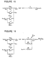
- the output TGHn of the control circuits SEL 0 to SEL 16 are "0", and the output TGMn is Mn, as will be understood from the truth table of Figure 14. Therefore, only one transfer gate TGMn selected in accordance with the content of the main bits D M3 to D M0 is selected, so that Vn is outputted from the output OUT.
- An equivalent circuit of the output circuit in this condition is shown in Figure 15.
- the resistance value "R” shows the on-resistance of the main transfer gates TGM 0 to TGM 16 and the resistance value "2R” shows the on-resistance of the sub transfer gates TGH 0 to TGH 16 .
- a multiple of different voltages can be generated by connecting the main transfer gates TG M 0 to TG M 16 and the sub transfer gates TG H 0 to TG H 16 in parallel to the gray scale level voltage supplies, and by turning on these transfer gates in various different combinations.
- the image input data D M3 to D M0 and D H1 and D H0 are transferred through the 6-bit shift registers 28a to 28k, and then latched into the 6-bit latches 29a to 29k in response to the latch pulse Vr.
- the AND gates AND 0a to AND 0k and AND 1a to AND 1k are controlled by the output voltage interpolating input Vh, so as to control application of the sub bits D H1 and D H0 to the output circuit.
- the relation between the image data and the output voltage as shown in the tables of Figures 19 and 20 can be obtained. Accordingly, operation similarly to the first embodiment can be performed, and the average current flowing through the gray scale level voltage supplied can be effectively reduced.
- the number of the transfer gates is increased, it is possible to increase the number of gray scale level voltages.
Landscapes
- Engineering & Computer Science (AREA)
- Physics & Mathematics (AREA)
- Computer Hardware Design (AREA)
- General Physics & Mathematics (AREA)
- Theoretical Computer Science (AREA)
- Chemical & Material Sciences (AREA)
- Crystallography & Structural Chemistry (AREA)
- Liquid Crystal Display Device Control (AREA)
- Liquid Crystal (AREA)
Claims (6)
- Flüssigkristallanzeige-Treiberschaltung, die folgendes aufweist:eine Vielzahl von Schalteinrichtungen (22a, 22b 22k), die jeweils ein erstes Ende aufweisen, das gemeinsam an einer Quellenleitung einer Flüssigkristallanzeigetafel angeschlossen ist, und ein zweites Ende, das jeweils an einer Vielzahl von Treiberspannungen (VR0, VR1, ..., VR16) angeschlossen ist, um eine unterschiedliche Spannung zur Quellenleitung zuzuführen, undeine Steuereinrichtung (20a, 20b 20k), die Bildeingabedaten zum selektiven Einschalten der Schalteinrichtungen empfängt, um eine Anzeige mit vielen Grautönen zu realisieren,wobei die Steuereinrichtung (20a, 20b 20k) Einrichtungen enthält, die basierend auf den Bildeingabedaten angeordnet sind, um nur eine Schalteinrichtung aus der Vielzahl von Schalteinrichtungen (22a, 22b 22k) während einer ersten Teilperiode einer horizontalen Anzeigeperiode einzuschalten und um wenigstens zwei Schalteinrichtungen aus der Vielzahl von Schalteinrichtungen (22a, 22b, ... 22k) während einer zweiten Teilperiode der einen horizontalen Anzeigeperiode gleichzeitig einzuschalten, wobei die wenigstens zwei Schalteinrichtungen die eine Schalteinrichtung enthalten, die während der ersten Teilperiode eingeschaltet ist,wobei die zweite Teilperiode von der ersten Teilperiode unterschiedlich ist und der ersten Teilperiode folgt.
- Flüssigkristallanzeige-Treiberschaltung nach Anspruch 1, wobei jede der Schalteinrichtungen (22a, 22b ..., 22k) eine Vielzahl von Schaltelementen (TG0, TG1, ..., TG16) enthält, und
wobei dann, wenn die Vielzahl von Schalteinrichtungen ausgewählt ist, die Steuereinrichtung (20a, 20b 20k) auf der Basis der Bildeingabedaten so steuert, daß eine Kombination von Schaltelementen, die in der Vielzahl der ausgewählten Schalteinrichtungen enthalten ist, eingeschaltet wird. - Flüssigkristallanzeige-Treiberschaltung nach Anspruch 1, wobei die zweite Teilperiode kürzer als die der ersten Teilperiode und die der einen horizontalen Anzeigeperiode ist.
- Flüssigkristallanzeige-Treiberschaltung nach Anspruch 3, wobei die erste Teilperiode eine Dauer von 2/3 von derjenigen der einen horizontalen Anzeigeperiode hat, und die zweite Teilperiode eine Dauer von etwa 1/3 von derjenigen der einen horizontalen Anzeigeperiode hat.
- Flüssigkristallanzeige-Treiberschaltung nach Anspruch 1, wobei während der ersten Teil periode nur die eine Schalteinrichtung ausgewählt wird, um einen Wert nahe einem vorbestimmten Sollwert auszuwählen, und eingeschaltet wird, und
wobei während der zweiten Teilperiode die eine Schalteinrichtung oder wenigstens einige der Vielzahl von Schalteinrichtungen gleichzeitig eingeschaltet werden, so daß der Sollspannungswert erhalten wird. - Flüssigkristallanzeige-Treiberschaltung nach Anspruch 1, wobei die nur eine Schalteinrichtung, die während der ersten Teilperiode eingeschaltet wird, durch einen Teil mit dem signifikantesten Bit (MSB) der Bildeingabedaten ausgewählt wird, wenn ein Teil mit dem am wenigsten signifikanten Bit (LSB) der Bildeingabedaten ein vorbestimmter Wert ist.
Applications Claiming Priority (2)
| Application Number | Priority Date | Filing Date | Title |
|---|---|---|---|
| JP4349887A JP2500417B2 (ja) | 1992-12-02 | 1992-12-02 | 液晶駆動回路 |
| JP349887/92 | 1992-12-02 |
Publications (2)
| Publication Number | Publication Date |
|---|---|
| EP0600499A1 EP0600499A1 (de) | 1994-06-08 |
| EP0600499B1 true EP0600499B1 (de) | 1997-09-24 |
Family
ID=18406785
Family Applications (1)
| Application Number | Title | Priority Date | Filing Date |
|---|---|---|---|
| EP93119471A Expired - Lifetime EP0600499B1 (de) | 1992-12-02 | 1993-12-02 | Steuerschaltung für Flüssigkristallanzeigevorrichtung |
Country Status (5)
| Country | Link |
|---|---|
| US (1) | US5534885A (de) |
| EP (1) | EP0600499B1 (de) |
| JP (1) | JP2500417B2 (de) |
| KR (1) | KR960016730B1 (de) |
| DE (1) | DE69314139T2 (de) |
Families Citing this family (15)
| Publication number | Priority date | Publication date | Assignee | Title |
|---|---|---|---|---|
| FR2708129B1 (fr) * | 1993-07-22 | 1995-09-01 | Commissariat Energie Atomique | Procédé et dispositif de commande d'un écran fluorescent à micropointes. |
| JPH08212793A (ja) * | 1994-11-29 | 1996-08-20 | Sanyo Electric Co Ltd | シフトレジスタおよび表示装置 |
| JP2715943B2 (ja) * | 1994-12-02 | 1998-02-18 | 日本電気株式会社 | 液晶表示装置の駆動回路 |
| CN100530332C (zh) * | 1995-02-01 | 2009-08-19 | 精工爱普生株式会社 | 液晶显示装置 |
| JP3367808B2 (ja) * | 1995-06-19 | 2003-01-20 | シャープ株式会社 | 表示パネルの駆動方法および装置 |
| JP3854329B2 (ja) * | 1995-12-27 | 2006-12-06 | シャープ株式会社 | マトリクス型表示装置の駆動回路 |
| KR100205371B1 (ko) * | 1996-03-26 | 1999-07-01 | 구자홍 | 액정의 다계화 구동회로 |
| TW376501B (en) * | 1998-01-26 | 1999-12-11 | Au Optronics Corp | Digital image driving circuit for LCD |
| KR100414647B1 (ko) * | 1998-11-30 | 2004-05-22 | 주식회사 대우일렉트로닉스 | 박막 트랜지스터-액정 화면용 게이트 드라이버 회로 |
| JP4747426B2 (ja) * | 2001-03-14 | 2011-08-17 | 日本テキサス・インスツルメンツ株式会社 | 駆動回路 |
| KR100456987B1 (ko) * | 2001-04-10 | 2004-11-10 | 가부시키가이샤 히타치세이사쿠쇼 | 표시 데이터를 표시하기 위한 표시 장치 및 표시 구동 장치 |
| JP4803902B2 (ja) * | 2001-05-25 | 2011-10-26 | 株式会社 日立ディスプレイズ | 表示装置 |
| KR20030066051A (ko) * | 2002-02-04 | 2003-08-09 | 일진다이아몬드(주) | 폴리 박막 트랜지스터를 이용한 액정 디스플레이 장치 |
| US7941336B1 (en) * | 2005-09-14 | 2011-05-10 | D2C Solutions, LLC | Segregation-of-duties analysis apparatus and method |
| JP2009008948A (ja) * | 2007-06-28 | 2009-01-15 | Nec Electronics Corp | データ線の駆動回路と駆動方法 |
Family Cites Families (4)
| Publication number | Priority date | Publication date | Assignee | Title |
|---|---|---|---|---|
| FR2633764B1 (fr) * | 1988-06-29 | 1991-02-15 | Commissariat Energie Atomique | Procede et dispositif de commande d'un ecran matriciel affichant des niveaux de gris |
| EP0458169A3 (en) * | 1990-05-15 | 1993-02-03 | Kabushiki Kaisha Toshiba | Drive circuit for active matrix type liquid crystal display device |
| EP0478386B1 (de) * | 1990-09-28 | 1995-12-13 | Sharp Kabushiki Kaisha | Steuerschaltung für ein Anzeigegerät |
| JPH04194896A (ja) * | 1990-11-28 | 1992-07-14 | Internatl Business Mach Corp <Ibm> | 階調表示方法及び装置 |
-
1992
- 1992-12-02 JP JP4349887A patent/JP2500417B2/ja not_active Expired - Lifetime
-
1993
- 1993-12-02 KR KR1019930026195A patent/KR960016730B1/ko not_active Expired - Fee Related
- 1993-12-02 EP EP93119471A patent/EP0600499B1/de not_active Expired - Lifetime
- 1993-12-02 US US08/162,734 patent/US5534885A/en not_active Expired - Lifetime
- 1993-12-02 DE DE69314139T patent/DE69314139T2/de not_active Expired - Fee Related
Also Published As
| Publication number | Publication date |
|---|---|
| JPH06175617A (ja) | 1994-06-24 |
| JP2500417B2 (ja) | 1996-05-29 |
| DE69314139T2 (de) | 1998-05-07 |
| DE69314139D1 (de) | 1997-10-30 |
| KR940015957A (ko) | 1994-07-22 |
| EP0600499A1 (de) | 1994-06-08 |
| US5534885A (en) | 1996-07-09 |
| KR960016730B1 (ko) | 1996-12-20 |
Similar Documents
| Publication | Publication Date | Title |
|---|---|---|
| US5617111A (en) | Circuit for driving liquid crystal device | |
| EP0600499B1 (de) | Steuerschaltung für Flüssigkristallanzeigevorrichtung | |
| US7400320B2 (en) | Digital/analog converter circuit, level shift circuit, shift register utilizing level shift circuit, sampling latch circuit, latch circuit and liquid crystal display device incorporating the same | |
| US8159486B2 (en) | Level converter circuit and a liquid crystal display device employing the same | |
| US7098882B2 (en) | Bidirectional shift register shifting pulse in both forward and backward directions | |
| USRE39366E1 (en) | Liquid crystal driver and liquid crystal display device using the same | |
| US7212183B2 (en) | Liquid crystal display apparatus having pixels with low leakage current | |
| US6747624B1 (en) | Driving circuit for supplying tone voltages to liquid crystal display panel | |
| US5196738A (en) | Data driver circuit of liquid crystal display for achieving digital gray-scale | |
| US6304241B1 (en) | Driver for a liquid-crystal display panel | |
| US6335721B1 (en) | LCD source driver | |
| US6191779B1 (en) | Liquid crystal display device, device for controlling drive of liquid crystal display device and D/A converting semiconductor device | |
| US7463234B2 (en) | Liquid crystal display and data latch circuit | |
| US6201523B1 (en) | Flat panel display device | |
| US6344814B1 (en) | Driving circuit | |
| WO1999014732A1 (en) | High density column drivers for an active matrix display | |
| US4736137A (en) | Matrix display device | |
| US7209057B2 (en) | Decode circuitry and a display device using the same | |
| US7245283B2 (en) | LCD source driving circuit having reduced structure including multiplexing-latch circuits | |
| US20060164368A1 (en) | Display apparatus with reduced power consumption in charging/discharging of data line | |
| KR100551738B1 (ko) | 액정표시장치의 구동회로 | |
| EP0493820B1 (de) | Treiberschaltung für eine Flüssigkristallanzeige | |
| US6727835B2 (en) | Analog multiplex level shifter with reset | |
| JPH0612027A (ja) | 液晶駆動回路 | |
| JP2006018087A (ja) | 画像表示装置 |
Legal Events
| Date | Code | Title | Description |
|---|---|---|---|
| PUAI | Public reference made under article 153(3) epc to a published international application that has entered the european phase |
Free format text: ORIGINAL CODE: 0009012 |
|
| 17P | Request for examination filed |
Effective date: 19940331 |
|
| AK | Designated contracting states |
Kind code of ref document: A1 Designated state(s): DE FR GB IT NL |
|
| 17Q | First examination report despatched |
Effective date: 19960327 |
|
| GRAG | Despatch of communication of intention to grant |
Free format text: ORIGINAL CODE: EPIDOS AGRA |
|
| GRAH | Despatch of communication of intention to grant a patent |
Free format text: ORIGINAL CODE: EPIDOS IGRA |
|
| GRAH | Despatch of communication of intention to grant a patent |
Free format text: ORIGINAL CODE: EPIDOS IGRA |
|
| GRAA | (expected) grant |
Free format text: ORIGINAL CODE: 0009210 |
|
| AK | Designated contracting states |
Kind code of ref document: B1 Designated state(s): DE FR GB IT NL |
|
| REF | Corresponds to: |
Ref document number: 69314139 Country of ref document: DE Date of ref document: 19971030 |
|
| ITF | It: translation for a ep patent filed | ||
| ET | Fr: translation filed | ||
| PLBE | No opposition filed within time limit |
Free format text: ORIGINAL CODE: 0009261 |
|
| STAA | Information on the status of an ep patent application or granted ep patent |
Free format text: STATUS: NO OPPOSITION FILED WITHIN TIME LIMIT |
|
| 26N | No opposition filed | ||
| PGFP | Annual fee paid to national office [announced via postgrant information from national office to epo] |
Ref country code: GB Payment date: 20011205 Year of fee payment: 9 |
|
| PGFP | Annual fee paid to national office [announced via postgrant information from national office to epo] |
Ref country code: FR Payment date: 20011212 Year of fee payment: 9 |
|
| PGFP | Annual fee paid to national office [announced via postgrant information from national office to epo] |
Ref country code: DE Payment date: 20011217 Year of fee payment: 9 |
|
| PGFP | Annual fee paid to national office [announced via postgrant information from national office to epo] |
Ref country code: NL Payment date: 20011228 Year of fee payment: 9 |
|
| REG | Reference to a national code |
Ref country code: GB Ref legal event code: IF02 |
|
| PG25 | Lapsed in a contracting state [announced via postgrant information from national office to epo] |
Ref country code: GB Free format text: LAPSE BECAUSE OF NON-PAYMENT OF DUE FEES Effective date: 20021202 |
|
| PG25 | Lapsed in a contracting state [announced via postgrant information from national office to epo] |
Ref country code: NL Free format text: LAPSE BECAUSE OF NON-PAYMENT OF DUE FEES Effective date: 20030701 Ref country code: DE Free format text: LAPSE BECAUSE OF NON-PAYMENT OF DUE FEES Effective date: 20030701 |
|
| GBPC | Gb: european patent ceased through non-payment of renewal fee | ||
| NLV4 | Nl: lapsed or anulled due to non-payment of the annual fee |
Effective date: 20030701 |
|
| PG25 | Lapsed in a contracting state [announced via postgrant information from national office to epo] |
Ref country code: FR Free format text: LAPSE BECAUSE OF NON-PAYMENT OF DUE FEES Effective date: 20030901 |
|
| REG | Reference to a national code |
Ref country code: FR Ref legal event code: ST |
|
| PG25 | Lapsed in a contracting state [announced via postgrant information from national office to epo] |
Ref country code: IT Free format text: LAPSE BECAUSE OF NON-PAYMENT OF DUE FEES Effective date: 20051202 |