EP0600501A1 - Dispositif semi-conducteur en résine moulée - Google Patents
Dispositif semi-conducteur en résine moulée Download PDFInfo
- Publication number
- EP0600501A1 EP0600501A1 EP93119473A EP93119473A EP0600501A1 EP 0600501 A1 EP0600501 A1 EP 0600501A1 EP 93119473 A EP93119473 A EP 93119473A EP 93119473 A EP93119473 A EP 93119473A EP 0600501 A1 EP0600501 A1 EP 0600501A1
- Authority
- EP
- European Patent Office
- Prior art keywords
- film
- island
- enveloper
- resin
- leads
- Prior art date
- Legal status (The legal status is an assumption and is not a legal conclusion. Google has not performed a legal analysis and makes no representation as to the accuracy of the status listed.)
- Withdrawn
Links
Images




Classifications
-
- H—ELECTRICITY
- H10—SEMICONDUCTOR DEVICES; ELECTRIC SOLID-STATE DEVICES NOT OTHERWISE PROVIDED FOR
- H10W—GENERIC PACKAGES, INTERCONNECTIONS, CONNECTORS OR OTHER CONSTRUCTIONAL DETAILS OF DEVICES COVERED BY CLASS H10
- H10W70/00—Package substrates; Interposers; Redistribution layers [RDL]
- H10W70/40—Leadframes
- H10W70/464—Additional interconnections in combination with leadframes
- H10W70/466—Tape carriers or flat leads
-
- H—ELECTRICITY
- H10—SEMICONDUCTOR DEVICES; ELECTRIC SOLID-STATE DEVICES NOT OTHERWISE PROVIDED FOR
- H10W—GENERIC PACKAGES, INTERCONNECTIONS, CONNECTORS OR OTHER CONSTRUCTIONAL DETAILS OF DEVICES COVERED BY CLASS H10
- H10W40/00—Arrangements for thermal protection or thermal control
- H10W40/70—Fillings or auxiliary members in containers or in encapsulations for thermal protection or control
- H10W40/77—Auxiliary members characterised by their shape
- H10W40/778—Auxiliary members characterised by their shape in encapsulations
-
- H—ELECTRICITY
- H10—SEMICONDUCTOR DEVICES; ELECTRIC SOLID-STATE DEVICES NOT OTHERWISE PROVIDED FOR
- H10W—GENERIC PACKAGES, INTERCONNECTIONS, CONNECTORS OR OTHER CONSTRUCTIONAL DETAILS OF DEVICES COVERED BY CLASS H10
- H10W74/00—Encapsulations, e.g. protective coatings
- H10W74/01—Manufacture or treatment
- H10W74/016—Manufacture or treatment using moulds
-
- H—ELECTRICITY
- H10—SEMICONDUCTOR DEVICES; ELECTRIC SOLID-STATE DEVICES NOT OTHERWISE PROVIDED FOR
- H10W—GENERIC PACKAGES, INTERCONNECTIONS, CONNECTORS OR OTHER CONSTRUCTIONAL DETAILS OF DEVICES COVERED BY CLASS H10
- H10W90/00—Package configurations
- H10W90/701—Package configurations characterised by the relative positions of pads or connectors relative to package parts
- H10W90/731—Package configurations characterised by the relative positions of pads or connectors relative to package parts of die-attach connectors
- H10W90/736—Package configurations characterised by the relative positions of pads or connectors relative to package parts of die-attach connectors between a chip and a stacked lead frame, conducting package substrate or heat sink
Definitions
- the present invention relates to a resin molded semiconductor device for a combination of a film carrier type semiconductor element and a lead frame.
- a film carrier type semiconductor element includes a film having a plurality of internal leads thereon, and a semiconductor chip contacted to inner portions of the internal leads.
- a lead frame includes an island for supporting the semiconductor chip, and a plurality of external leads. The film carrier type semiconductor element is assembled into the lead frame by contacting the semiconductor chip to the island and by connecting the outer portions of the internal leads to the external leads, to complete a semiconductor assembly.
- the above-mentioned semiconductor assembly is sandwiched by two metal molds, so that the semiconductor assembly is located in a cavity between the metal molds. Then, hot resin is injected into the cavity, and the injected resin is cooled and hardened by the metal molds, to thereby form an enveloper made of resin for the semiconductor assembly. Thus, a resin molded semiconductor is completed, which will be explained later in more detail.
- the island since a lower cavity below the island is remarkably larger than an upper cavity above the film, so that the amount of resin injected into the lower cavity is remarkably larger than that injected into the upper cavity at an initial stage of injection of resin, the island may be moved up by the pressure of the resin injected into the lower cavity. Simultaneously, since the island is wider than the film, so that resin is hardly injected into a middle cavity between the film and the island, the film may be moved down by the pressure of resin injected into the upper cavity.
- an edge of the semiconductor chip may be in contact with an inner portion of one of the internal leads, thus inviting a short circuit. Also, the injected resin may be cracked, thus deteriorating the reliability of the resin molded semiconductor device.
- a film carrier type semiconductor element includes a film, internal leads adhered thereto, and a semiconductor chip contacted to inner portions of the internal leads.
- a lead frame includes an island and external leads.
- the film carrier semiconductor element is assembled in the lead frame by contacting the semiconductor chip to the island and by connecting outer portions of the internal leads to the external leads.
- An enveloper made of resin encapusulates the film carrier type semiconductor element and a part of the external leads.
- the thickness of resin from the island to a rear face of the enveloper is substantially the same as that from the film to a front face of the enveloper.
- the island is narrower than the film.
- the pressure of resin between the film and the island is increased, and as a result, the amount of moving-down of the film is reduced.
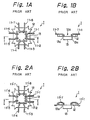
- a film carrier type semiconductor element 1 is prepared.
- the film carrier type semiconductor element 1 is manufactured by adhering a lead pattern of internal leads 11-1, 11-2, ..., and 11-8 made of copper foil or the like, to an insulating film carrier tape (not shown) made of polyimid or the like and which includes a film 12 as a part thereof.
- a semiconductor chip 13 is mounted on the film carrier tape via a device hole 12a, and metal protrusions, i.e., bumps 13a of the semiconductor chip 13 are bonded to inner portions of the internal leads 11-1, 11-2, ..., and 11-8 using a thermal pressure method or a eutectic method. Then, the film carrier tape and the outer portions internal leads 11-1, 11-2, ..., and 11-8 are cut by a cut mold, to thereby complete the film carrier type semiconductor element 1 as illustrated in Figs. 1A and 1B.
- Fig. 2A and Fig. 2B which is a cross-sectional view taken along the II - II of Fig. 2A, the outer portions of the internal leads 11-1, 11-2, ..., and 11-8 are bent down by using a pressing tool (not shown).
- a lead frame 2 made of metal such as copper is prepared.
- the lead frame 2 includes external leads 21-1, 21-2, ..., and 21-8, four suspenders 22-1, 22-2, 22-3 and 22-4, and an island 23 suspended by the suspenders 22-1, 22-2, 22-3 and 22-4.
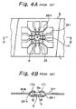
- the film carrier type semiconductor element 1 of Figs. 2A and 2B is mounted on the lead frame of Figs. 3A and 3B, thus obtaining a semiconductor assembly.
- the outer portions of the internal leads 11'-1, 11'-2, ..., and 11'-8 are bonded to the inner portions of the external leads 21-1, 21-2, ..., and 21-8, respectively, by using a thermal pressure method or a eutectic method.
- the semiconductor chip 13 is bonded to the island 23 by an adhesive member 3 which is hardened by a heat treatment.
- the semiconductor device of Figs. 4A and 4B is sandwiched by a lower metal mold 4-1 and 4-2. Then, hot resin is injected into a cavity between the lower metal mold 4-1 and the upper metal mold 4-2, as indicated in the figure by an arrow.
- Fig. 6A and Fig. 6B which is a cross-sectional view taken along the line VI - VI of Fig. 6A
- the lower metal mold 4-1 and the upper metal mold 4-2 are removed, and as a result, an enveloper 5 made of resin encapsulates the semiconductor assembly.
- probes are in contact with the external leads 21-1, 21-2, ..., and 21-8, to thereby carry out a test, thus completing a resin molded semiconductor device.
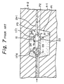
- a cavity between the lower metal mold 4-1 and the upper metal mold 4-2 is divided into three partitions P1, P2 and P3 before the injection of resin.
- the partition P1 is defined by the lower metal mold 4-1 and the island 23;
- the partition P2 is defined by the island 23 and the film 12 (and the semiconductor chip 13);
- the partition P3 is defined by the film 12 (and the semiconductor chip) and the upper metal mold 4-2.
- the film 12 may be moved down as indicated by an arrow Y.
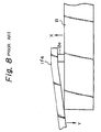
- an edge of the semiconductor chip 13 may be in contact with an inner portion of the internal lead such as 11'-6, as illustrated in Fig. 8.
- a short-circuit may occur between the semiconductor chip 13 and the internal leads.
- the moving-up of the island 23 and the moving-down of the film 12 may break the injected resin, thus deteriorating the reliability thereof.
- the moving-up of the island 23 and/or the moving-down of the film 12 are suppressed.
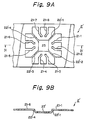
- a lead frame 2' has a narrower island 23' than the island 23 of Figs. 3A and 3B, and accordingly, has suspenders 22'-1, 22'-2, 22'-3 and 22'-4 longer than the suspenders 22-1, 22-2, 22-3 and 22-4 of Figs. 3A and 3B.
- the island 23' is narrower than the film 12 of the film carrier type semiconductor element 1 of Figs. 1A and 1B.
- Figs. 10A and 10B which correspond to Figs. 4A and 4B, respectively, the film carrier type semiconductor element 1 of Figs. 1A and 1B is mounted on the lead frame 2' of Figs. 4A and 4B, thus completing a semiconductor assembly.
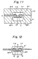
- Fig. 11 which corresponds to Fig. 5, the semiconductor device of Figs. 10A and 10B are sandwiched by the lower metal mold 4-1 and the upper metal mold 4-2, and hot resin is injected into a cavity between the lower metal mold 4-1 and the upper metal mold 4-2.
- Fig. 12 which corresponds to Fig. 6B, the lower metal mold 4-1 and the upper metal mold 4-2 are removed, and as a result, an enveloper 5' made of resin encapsulates the semiconductor assembly. Thus, a resin molded semiconductor device is completed.
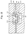
- Fig. 13 which explains an effect of the resin molded semiconductor device according to the first embodiment of the present invention
- a space or distance D1' between the lower metal mold 4-1 and the island 23' is only slightly larger than a space or distance D2' between the film 12 and the upper metal mold 4-2, for example, a ratio D1'/D2' is 1.1
- the amount of resin injected into the partition P1 is slightly larger than the amount of resin injected into the partition P3 at an initial stage of injection of resin, as illustrated in Fig. 13.
- the island 23' having the semiconductor chip 13 mounted thereon is hardly moved up.
- the island 23' is narrower than the film 12, i.e., since the width D3' of the island 23' is smaller than the width of the film 13, resin is smoothly injected into the partition P2. Therefore, the amount of resin injected into the partition P3 is not much larger than the amount of resin injected into the partition P2 at an initial stage of injection of resin, as illustrated in Fig. 13. As a result, the film 12 is hardly moved down.
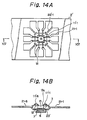
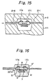
- Figs. 14A and 14B which correspond to Figs. 10A and 10B, respectively, the film carrier type semiconductor element 1 of Figs. 2A and 2B is mounted on the lead frame 2' of Figs. 4A and 4B.
- a heat dissipation plate 6 is adhered by a polyimid member 7 to a rear face of the island 23'.
- Fig. 15 which corresponds to Fig. 11, the semiconductor device of Figs. 14A and 14B is sandwiched by the lower metal mold 4-1 and the upper metal mold 4-2, and hot resin is injected into a cavity between the lower metal mold 4-1 and the upper metal mold 4-2.
- Fig. 16 which corresponds to Fig. 12, the lower metal mold 4-1 and the upper metal mold 4-2 are removed, and as a result, an enveloper 5'' made of resin encapsulates the semiconductor device. Thus, a resin molded semiconductor device is completed.
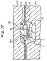
- Fig. 17 which explains an effect of the resin molded semiconductor device according to the second embodiment of the present invention
- a space or distance D1'' between the lower metal mold 4-1 and the heat dissipation member 6 is only slightly larger than a space or distance D2'' between the film 12 and the upper metal mold 4-2, for example, a ratio D1''/D2'' is 1.1
- the amount of resin injected into the partition P1 is slightly larger than the amount of resin injected into the partition P3 at an initial stage of injection of resin, as illustrated in Fig. 17.
- the island 23' mounting the semiconductor chip 13 is hardly moved up.
- the island 23' is narrower than the film 12, i.e., since the width D3'' of the island 23' is smaller than the width of the film 13, resin is smoothly injected in the partition P2. Therefore, the amount of resin injected into the partition P3 is not much larger than the amount of resin injected into the partition P2 at an initial stage of injection of resin, as illustrated in Fig. 17. As a result, the film 12 is hardly moved down.
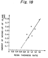
- the amount of moving up of the island 23 (23') is dependent upon a resin thickness ratio defined by the space or distance D1 (D1', D1'') between the rear face of the island 23' (or the heat dissipation member 6) and the lower metal mold 4-1 to the space or distance D2 (D2', D2'') between the film 23 and the upper metal mold 4-2.
- a resin thickness ratio defined by the space or distance D1 (D1', D1'') between the rear face of the island 23' (or the heat dissipation member 6) and the lower metal mold 4-1 to the space or distance D2 (D2', D2'') between the film 23 and the upper metal mold 4-2.
- the resin thickness ratio is less than 1.1
- the amount of moving-up of the island 23' is less than 0.4mm.
- the resin thickness ratio is made 1.0 to 1.6, preferably, a value close to 1.0, such as 1.0 to 1.1.
- the amount of moving-down of the film 12 is 0.54mm, and if the ratio of the width D3 (D3', D3'') of the island 23 (23') to the width D4 (D4', D4'') of the film 12 is 0.534, the amount of moving down of the film 12 is approximately 0mm (neglible).
Landscapes
- Encapsulation Of And Coatings For Semiconductor Or Solid State Devices (AREA)
- Lead Frames For Integrated Circuits (AREA)
- Structures Or Materials For Encapsulating Or Coating Semiconductor Devices Or Solid State Devices (AREA)
- Wire Bonding (AREA)
Applications Claiming Priority (2)
| Application Number | Priority Date | Filing Date | Title |
|---|---|---|---|
| JP323887/92 | 1992-12-03 | ||
| JP4323887A JPH06177283A (ja) | 1992-12-03 | 1992-12-03 | 樹脂封止型半導体装置 |
Publications (1)
| Publication Number | Publication Date |
|---|---|
| EP0600501A1 true EP0600501A1 (fr) | 1994-06-08 |
Family
ID=18159715
Family Applications (1)
| Application Number | Title | Priority Date | Filing Date |
|---|---|---|---|
| EP93119473A Withdrawn EP0600501A1 (fr) | 1992-12-03 | 1993-12-02 | Dispositif semi-conducteur en résine moulée |
Country Status (2)
| Country | Link |
|---|---|
| EP (1) | EP0600501A1 (fr) |
| JP (1) | JPH06177283A (fr) |
Cited By (1)
| Publication number | Priority date | Publication date | Assignee | Title |
|---|---|---|---|---|
| WO1996013068A1 (fr) * | 1994-10-19 | 1996-05-02 | Telefonaktiebolaget Lm Ericsson | Injection d'un materiau d'encapsulage sur un composant optoelectronique |
Families Citing this family (2)
| Publication number | Priority date | Publication date | Assignee | Title |
|---|---|---|---|---|
| JPH0888312A (ja) * | 1994-09-14 | 1996-04-02 | Nec Corp | 樹脂封止型半導体装置 |
| JP3483238B2 (ja) * | 1997-08-29 | 2004-01-06 | 三井金属鉱業株式会社 | フィルムキャリアおよびこれを用いたフィルムキャリアデバイス |
Citations (6)
| Publication number | Priority date | Publication date | Assignee | Title |
|---|---|---|---|---|
| JPS60119756A (ja) * | 1983-12-01 | 1985-06-27 | New Japan Radio Co Ltd | 半導体装置の製造方法 |
| JPS61184855A (ja) * | 1985-02-13 | 1986-08-18 | Oki Electric Ind Co Ltd | 樹脂封止形半導体装置 |
| JPH02271648A (ja) * | 1989-04-13 | 1990-11-06 | Matsushita Electric Ind Co Ltd | 樹脂モールド電子部品及びその成形金型 |
| JPH0394435A (ja) * | 1989-09-06 | 1991-04-19 | Toshiba Corp | 半導体装置 |
| JPH0395959A (ja) * | 1989-09-07 | 1991-04-22 | Shinko Electric Ind Co Ltd | リードフレーム |
| JPH04316356A (ja) * | 1991-04-15 | 1992-11-06 | Mitsubishi Electric Corp | 樹脂封止形半導体装置 |
Family Cites Families (1)
| Publication number | Priority date | Publication date | Assignee | Title |
|---|---|---|---|---|
| JP2661442B2 (ja) * | 1991-12-03 | 1997-10-08 | 日本電気株式会社 | 樹脂封止型半導体装置及びその製造方法 |
-
1992
- 1992-12-03 JP JP4323887A patent/JPH06177283A/ja active Pending
-
1993
- 1993-12-02 EP EP93119473A patent/EP0600501A1/fr not_active Withdrawn
Patent Citations (6)
| Publication number | Priority date | Publication date | Assignee | Title |
|---|---|---|---|---|
| JPS60119756A (ja) * | 1983-12-01 | 1985-06-27 | New Japan Radio Co Ltd | 半導体装置の製造方法 |
| JPS61184855A (ja) * | 1985-02-13 | 1986-08-18 | Oki Electric Ind Co Ltd | 樹脂封止形半導体装置 |
| JPH02271648A (ja) * | 1989-04-13 | 1990-11-06 | Matsushita Electric Ind Co Ltd | 樹脂モールド電子部品及びその成形金型 |
| JPH0394435A (ja) * | 1989-09-06 | 1991-04-19 | Toshiba Corp | 半導体装置 |
| JPH0395959A (ja) * | 1989-09-07 | 1991-04-22 | Shinko Electric Ind Co Ltd | リードフレーム |
| JPH04316356A (ja) * | 1991-04-15 | 1992-11-06 | Mitsubishi Electric Corp | 樹脂封止形半導体装置 |
Non-Patent Citations (6)
| Title |
|---|
| PATENT ABSTRACTS OF JAPAN vol. 009, no. 277 (E - 355) 6 November 1985 (1985-11-06) * |
| PATENT ABSTRACTS OF JAPAN vol. 011, no. 007 (E - 469) 9 January 1987 (1987-01-09) * |
| PATENT ABSTRACTS OF JAPAN vol. 015, no. 026 (E - 1025) 22 January 1991 (1991-01-22) * |
| PATENT ABSTRACTS OF JAPAN vol. 015, no. 277 (E - 108) 15 July 1991 (1991-07-15) * |
| PATENT ABSTRACTS OF JAPAN vol. 015, no. 280 (E - 109) 16 July 1991 (1991-07-16) * |
| PATENT ABSTRACTS OF JAPAN vol. 017, no. 150 (E - 1339) 25 March 1993 (1993-03-25) * |
Cited By (2)
| Publication number | Priority date | Publication date | Assignee | Title |
|---|---|---|---|---|
| WO1996013068A1 (fr) * | 1994-10-19 | 1996-05-02 | Telefonaktiebolaget Lm Ericsson | Injection d'un materiau d'encapsulage sur un composant optoelectronique |
| US6326680B1 (en) | 1994-10-19 | 2001-12-04 | Telefonaktiebolaget Lm Ericsson (Publ) | Injection of encapsulating material on a optocomponent |
Also Published As
| Publication number | Publication date |
|---|---|
| JPH06177283A (ja) | 1994-06-24 |
Similar Documents
| Publication | Publication Date | Title |
|---|---|---|
| JP2849594B2 (ja) | 電子モジュールの封止方法 | |
| US4598307A (en) | Integrated circuit device having package with bypass capacitor | |
| US4822988A (en) | Card containing a component and a micromodule having side contacts | |
| EP0390996A2 (fr) | Module de carte de circuit intégré | |
| US4246697A (en) | Method of manufacturing RF power semiconductor package | |
| JP2524606B2 (ja) | メモリ―・カ―ドを製造する方法 | |
| JPH06244360A (ja) | 半導体装置 | |
| EP0329459A2 (fr) | Support à puce moulé | |
| JPS62209844A (ja) | 封入式テ−プ自動接着化集積回路モジユ−ルのための表面装着自在包装装置 | |
| US6177720B1 (en) | Method of manufacturing a semiconductor device with a pair of radiating terminals and a plurality of lead terminals formed from a single lead frame | |
| EP0600501A1 (fr) | Dispositif semi-conducteur en résine moulée | |
| EP0438165B1 (fr) | Parties de dispositif semi-conducteur | |
| US5105261A (en) | Semiconductor device package having particular lead structure for mounting multiple circuit boards | |
| JPS58173853A (ja) | 集積回路用容器の製造方法及びダイス−ヒ−トシンク組合せ | |
| CN213401185U (zh) | 一种防弯折变形的引线框架及封装料片 | |
| JP2829567B2 (ja) | チップマウント型led | |
| KR20010022252A (ko) | 칩 모듈 제조방법 | |
| JPH01120856A (ja) | リードフレーム | |
| JP2574605Y2 (ja) | 複合半導体装置 | |
| JP3126782B2 (ja) | 薄型半導体装置の製造方法 | |
| JPH02268471A (ja) | 光送受信モジュール用リードフレーム | |
| JPH01164056A (ja) | リードフレーム | |
| JPH10163376A (ja) | 高周波電力用半導体装置 | |
| JP2917556B2 (ja) | 絶縁物封止型電子部品の製造方法 | |
| JPS6334510B2 (fr) |
Legal Events
| Date | Code | Title | Description |
|---|---|---|---|
| PUAI | Public reference made under article 153(3) epc to a published international application that has entered the european phase |
Free format text: ORIGINAL CODE: 0009012 |
|
| 17P | Request for examination filed |
Effective date: 19940318 |
|
| AK | Designated contracting states |
Kind code of ref document: A1 Designated state(s): DE FR GB |
|
| 17Q | First examination report despatched |
Effective date: 19950912 |
|
| STAA | Information on the status of an ep patent application or granted ep patent |
Free format text: STATUS: THE APPLICATION HAS BEEN WITHDRAWN |
|
| 18W | Application withdrawn |
Withdrawal date: 19980209 |