EP0600643A2 - Anordnung, die einen ballistischen Heteroübergang-Transistor enthält - Google Patents
Anordnung, die einen ballistischen Heteroübergang-Transistor enthält Download PDFInfo
- Publication number
- EP0600643A2 EP0600643A2 EP93309227A EP93309227A EP0600643A2 EP 0600643 A2 EP0600643 A2 EP 0600643A2 EP 93309227 A EP93309227 A EP 93309227A EP 93309227 A EP93309227 A EP 93309227A EP 0600643 A2 EP0600643 A2 EP 0600643A2
- Authority
- EP
- European Patent Office
- Prior art keywords
- base
- transistor
- emitter
- frequency
- collector
- Prior art date
- Legal status (The legal status is an assumption and is not a legal conclusion. Google has not performed a legal analysis and makes no representation as to the accuracy of the status listed.)
- Granted
Links
Images


Classifications
-
- H—ELECTRICITY
- H10—SEMICONDUCTOR DEVICES; ELECTRIC SOLID-STATE DEVICES NOT OTHERWISE PROVIDED FOR
- H10D—INORGANIC ELECTRIC SEMICONDUCTOR DEVICES
- H10D10/00—Bipolar junction transistors [BJT]
- H10D10/80—Heterojunction BJTs
- H10D10/821—Vertical heterojunction BJTs
Definitions
- This application pertains to heterojunction bipolar transistors (HBTs).
- the cut-off frequency f r (defined as the frequency at which the current gain ( ⁇ , i.e., the absolute value of the parameter h fe ⁇ ⁇ J c / ⁇ J B , is unity) is used as a figure of meritthat is indicative of the high frequency capability of a transistor. See for instance, S. M. Sze, "Physics of Semiconductor Devices", 2nd Edition, John Wiley & Sons, 1981, Chapter 3. It is well known that ( ⁇ at high frequencies decreases at a value of 10 dB/decade.
- Another parameter that can be used to characterize the high frequency capabilities of a (typically microwave) transistor is the unilateral (power) gain U. See S. M. Sze, op. cit, pp. 160-165.
- the frequency at which the unilateral gain is unity is the maximum oscillating frequency fmax, which can, but need not, be larger than f T .
- f max is conventionally determined by extrapolation of the measured roll-off in h fe and U, respectively.
- G. T. Wright (see, for instance, Solid State Electronics, Vol. 22, p. 399, 1979) proposed extension of active transistor operation to frequencies beyond the conventional cutoff frequency f T .
- the proposal involved the utilization of transit time resonances that arise from carrier drift in the collector space charge region.
- the proposed model suggested for an ideal transistor (i.e., a transistor without any parasitic impedances) the possibility that
- S. Tiwari IEEE Electron Device Letter, Vol. 10, No. 12, p.
- HBTs with substantially collisionless base transport are known. See, for instance, U. S. patent 4,819,343.
- free carrier (not necessarily electron) base transport is considered to be "ballistic" if the mean free path (A) of the carriers in the base material is ⁇ W B , the base width.
- the mean free path can, at least in principle, be determined by transport measurements in a magnetic field.
- the cut-off frequency of a prior art ballistic HBT cannot be less than (2 ⁇ B ) -1 , where ⁇ B is the average base transit time of the minority carriers. Therefore, prior art ballistic HBTs are typically designed to minimize ⁇ B . This generally involves maximizing carrier velocity through choice of low effective mass minority carriers (almost invariably resulting in the choice of n-p-n III/V transistors), and through choice of a design that exhibits a relatively large value of the parameter A, the injection energy. It also typically involves minimization of the base width W B .
- the invention is as defined by the claims. Broadly speaking, the invention is a novel HBT that can exhibit power gain (preferably also current gain) at frequencies above the conventionally defined f r and fmax.
- the invention typically is embodied in an article that comprises a HBT that compromises first, second and third semiconductor regions, to be referred to as emitter, base and collector, respectively.
- the article also comprises means for electrically contacting the emitter, base and collector, respectively.
- the base is intermediate the emitter and collector and has a width W B
- the emitter and collector each comprises material of a first conductivity type, and the base comprises material of a second conductivity type.
- Associated with the transistor is a current gain ( ⁇ , a unilateral power gain U, and conven-] tional cut-off frequences f T and f max .
- the transistor is selected such that ⁇ B is less than about 0.5 ⁇ B , where ⁇ B is the variance of ⁇ B , and such that the absolute value of U is greater than unity at least at one frequency above f max and f T .
- the minority carriers are injected to the base over a (typically relatively abrupt) barrier, with the average injection energy A of the carriers being selected such that kT ⁇ ⁇ h ⁇ oPt , where k is the Boltz- mann constant, T is the absolute temperature of the transistor during operation, h is Planck's constant, and ⁇ oPt is the frequency of the lowest optical phonon in the base material.
- A a 3 kT. Since h ⁇ oPt is, exemplarily, about 59 meV in Si and about 38 meV in GaAs, it can be readily seen that typically T ⁇ 77 K.
- a significant aspect of the invention is substantially collimated (in the forward direction) injection of substantially mono-energetic minority carriers into the base, and substantially ballistic transport of these carriers through the base to the base/collector junction.
- ⁇ B is much less than ⁇ B (preferably, ⁇ B ⁇ ⁇ B /5) where ⁇ B is the average base transit time for the carriers, and ⁇ B is the variance of ⁇ B .
- Operation of the transistor at cryogenic temperatures, together with the choice of injection energy less than the energy of any relevant optical phonon call result in a ballistic scattering length (herein equivalent to A) of about 100 nm or even more.
- ⁇ B typically is proportional to T, as those skilled in the art know.
- the condition that ⁇ B is substantially less than ⁇ B can, in general, be readily met by appropriate choice of operating temperature.
- the quantities i B and ⁇ B thus are well defined and also determinable for any particular transistor according to the invention. For instance, for the typical case of a thermal distribution of carriers on the top of the barrier, it is known that ( ⁇ B / ⁇ B ) is approximately equal to (kT/2A).
- a HTB that meets the fundamental requirement ⁇ B « i B will herein be referred to as a "coherent" transistor (CT) since, in such a device, a minority carrier pulse experiences relatively little dispersion during its propagation through the base.
- CT coherent transistor
- a CT can exhibit (current and/or power) gain at frequencies about f r and f max , thus making possible operation at previously unattainable frequences.
- the magnitude of the resonance peaks decreases with frequency as 2(2 ⁇ f n ⁇ B ) -2 .
- the above described properties are modified to some extent.
- the positions of the resonant peaks in the current gain are no longer simple multiples of f T .
- the basic advantage of the CT namely the possibility of providing gain at a frequency above f T and f max , is preserved.
- FIG. 1 schematically depicts the band diagram of an abrupt-junction HBT that can, assuming an appropriate choice of parameters, advantageously embody the invention.
- an "abrupt-junction" HBT we mean herein a HBT in which the width of the emitter/base junction "transition" region is small, typically no more than 0.1 W B , frequently only a few crystal layers.
- the "transition” region is the region in which the relevant band edge drops from the peak of the emitter/base energy barrier to the constant base value.
- the exemplary band diagram corresponds to a conventionally biased n-p-n HBT.
- Numerals 11-13 designate emitter, base and collector, respectively.
- the base has width W B , a voltage V BE is applied between base and emitter, and a voltage - V BC is applied between base and collector. Minority carriers (i.e. electrons in the instant case) are injected into the base over a (desirably abrupt) energy barrier of height A.
- Minority carriers i.e. electrons in the instant case
- An analogous band diagram can readily be drawn for a p-n-p HBT according to the invention.
- the gain peaks occur approximately at f n , their magnitude decreasing with frequency as 1/f 2 n . It can be shown that, underthe stated conditions, the maximum current gain of the nth peak ( ⁇ n is approximately equal to
- the figure clearly demonstrates the existence in the CT of the large gain in the frequency range in which not only the diffusive transistor but even the transistor with no base delay at all, are completely damped.
- FIG. 4 represents an appropriate equivalent circuit of an abrupt junction HBT, wherein dashed line 40 encloses the intrinsic portion of the transistor, and E, B and C refer to emitter, base and collector, respectively.
- the intrinsic parameters R E and C E are the differential resistance and capacitance of the emitter/base junction, respectively, C c and g A are the collector junction capacitance and the Early conductance, respectively, ⁇ B and ⁇ c are the base and collector transport factors, respectively, and R B is the intrinsic base resistance.
- C cx is the extrinsic collector capacitance, and R cx and R EX are the parasitic base, collector and emitter resistances.
- phase delay is associated with the current transport through any bipolar transistor.
- a CT will typically be designed such that ⁇ ⁇ 0, with ⁇ B ⁇ 2 ⁇ f ⁇ B ⁇ forfrequen- cies above f r and f max . This implies design choices that are contrary to the prior art teachings.
- the emitter phase angle ⁇ E is defined only in the limit ⁇ E « (typically ⁇ E ⁇ ⁇ /4), and in that limit is approximately equal to 2 ⁇ fR e C e .
- FIG. 5 schematically shows relevant aspects of an exemplary CT, wherein numerals 50-56 refer, respectively, to the collector contact, collector, collector depletion region, base, emitter, emitter contact and base contact. Numeral 540 refers to the emitter/base space charge layer. The emitter stripe with L E , base width W B and collector depletion layer with W c are also indicated. The relevant characteristics of a CT as shown in FIG. 5 were determined from the equivalent circuit of FIG.
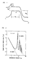
- FIG. 6 shows results of the numerical analysis. In particular, it shows the absolute values of current gain and unilateral power gain, both as a function of frequency.
- the conventional f T of the exemplary transistor is about 100 GHz.
- the figure shows, however, that the transistor is active up to frequencies of about 2 ⁇ f T .
- the analysis revealed that the current gain is largely damped away by the parasitics (although a trace of the peak is clearly seen nearf ⁇ B ⁇ 1), and that the unilateral power gain U in the region between the two peaks in
- An abrupt junction CT of design substantially as shown in FIG. 5 is made as follows: on a conventional single crystal Si substrate is grown by conventional MBE an epitaxial layer sequence that comprises a 200 nm thick n-type (10 19 cm- 3 B) collector layer, a 100 nm thick substantially undoped ( ⁇ 10 16 CM -3 ) collector depletion layer, a 100 nm thick p-type (10 19 cm-3 As) Si 1-x Ge x (X ⁇ 0.1) base layer, a 5 nm thick light p-type ( ⁇ 10 17 cm- 3 As) Si emitter/base spaced charge layer, and a 200 nm thick n-type (10 19 cm- 3 B) emitter layer.
- the wafer is patterned by conventional lithography and etching to define a HBT, and emitter, base and collector contacts are provided, all as known in the art.
- the HBT is cooled to 4.2K and conventional measurements are carried out.
- the measurements show that the device is a CT, and ⁇ and U substantially as shown in FIG. 6. Measurements at 15K show little change in behavior. This temperature can readily be reached by means of a commercially available re-circulating He-refrigerator.
Landscapes
- Bipolar Transistors (AREA)
Applications Claiming Priority (2)
| Application Number | Priority Date | Filing Date | Title |
|---|---|---|---|
| US981588 | 1992-11-25 | ||
| US07/981,588 US5304816A (en) | 1992-11-25 | 1992-11-25 | Article comprising a "ballistic" heterojunction bipolar transistor |
Publications (3)
| Publication Number | Publication Date |
|---|---|
| EP0600643A2 true EP0600643A2 (de) | 1994-06-08 |
| EP0600643A3 EP0600643A3 (de) | 1995-01-11 |
| EP0600643B1 EP0600643B1 (de) | 2001-07-11 |
Family
ID=25528491
Family Applications (1)
| Application Number | Title | Priority Date | Filing Date |
|---|---|---|---|
| EP93309227A Expired - Lifetime EP0600643B1 (de) | 1992-11-25 | 1993-11-18 | Verfahren zum Betrieb eines ballistischen Heteroübergang-Transistors |
Country Status (4)
| Country | Link |
|---|---|
| US (1) | US5304816A (de) |
| EP (1) | EP0600643B1 (de) |
| JP (1) | JP2851994B2 (de) |
| DE (1) | DE69330420T2 (de) |
Cited By (1)
| Publication number | Priority date | Publication date | Assignee | Title |
|---|---|---|---|---|
| DE19824110A1 (de) * | 1998-05-29 | 1999-12-09 | Daimler Chrysler Ag | Resonanz Phasen Transistor mit Laufzeitverzögerung |
Families Citing this family (2)
| Publication number | Priority date | Publication date | Assignee | Title |
|---|---|---|---|---|
| JP2005229074A (ja) * | 2004-02-16 | 2005-08-25 | Toshiba Corp | バイポーラ型トランジスタ |
| US7902635B2 (en) * | 2005-07-11 | 2011-03-08 | Wisconsin Alumni Research Foundation | High-power-gain, bipolar transistor amplifier |
Family Cites Families (9)
| Publication number | Priority date | Publication date | Assignee | Title |
|---|---|---|---|---|
| US4866488A (en) * | 1985-03-29 | 1989-09-12 | Texas Instruments Incorporated | Ballistic transport filter and device |
| GB8708926D0 (en) * | 1987-04-14 | 1987-05-20 | British Telecomm | Bipolar transistor |
| US4829343A (en) * | 1987-07-17 | 1989-05-09 | American Telephone & Telegraph Company, At&T Bell Laboratories | Hot electron transistor |
| US4958208A (en) * | 1987-08-12 | 1990-09-18 | Nec Corporation | Bipolar transistor with abrupt potential discontinuity in collector region |
| CA1303754C (en) * | 1988-09-07 | 1992-06-16 | American Telephone And Telegraph Company | Bipolar hot electron transistor |
| US5206524A (en) * | 1988-09-28 | 1993-04-27 | At&T Bell Laboratories | Heterostructure bipolar transistor |
| US5198689A (en) * | 1988-11-30 | 1993-03-30 | Fujitsu Limited | Heterojunction bipolar transistor |
| DE69032597T2 (de) * | 1990-02-20 | 1999-03-25 | Kabushiki Kaisha Toshiba, Kawasaki, Kanagawa | Bipolartransistor mit Heteroübergang |
| JPH0669220A (ja) * | 1991-10-09 | 1994-03-11 | Furukawa Electric Co Ltd:The | ヘテロ接合GaAs系バイポーラトランジスタ |
-
1992
- 1992-11-25 US US07/981,588 patent/US5304816A/en not_active Expired - Lifetime
-
1993
- 1993-11-18 EP EP93309227A patent/EP0600643B1/de not_active Expired - Lifetime
- 1993-11-18 DE DE69330420T patent/DE69330420T2/de not_active Expired - Lifetime
- 1993-11-22 JP JP5314018A patent/JP2851994B2/ja not_active Expired - Lifetime
Cited By (2)
| Publication number | Priority date | Publication date | Assignee | Title |
|---|---|---|---|---|
| DE19824110A1 (de) * | 1998-05-29 | 1999-12-09 | Daimler Chrysler Ag | Resonanz Phasen Transistor mit Laufzeitverzögerung |
| US6255674B1 (en) | 1998-05-29 | 2001-07-03 | Daimlerchrysler Ag | Silicon-germanium heterobipolar transistor with a step-wise graded base |
Also Published As
| Publication number | Publication date |
|---|---|
| DE69330420D1 (de) | 2001-08-16 |
| US5304816A (en) | 1994-04-19 |
| EP0600643A3 (de) | 1995-01-11 |
| JP2851994B2 (ja) | 1999-01-27 |
| EP0600643B1 (de) | 2001-07-11 |
| JPH06216147A (ja) | 1994-08-05 |
| DE69330420T2 (de) | 2002-05-23 |
Similar Documents
| Publication | Publication Date | Title |
|---|---|---|
| Ishibashi et al. | A possible near-ballistic collection in an AlGaAs/GaAs HBT with a modified collector structure | |
| Kurishima et al. | Fabrication and characterization of high-performance InP/InGaAs double-heterojunction bipolar transistors | |
| US5006912A (en) | Heterojunction bipolar transistor with SiGe | |
| US6025615A (en) | Microwave heterojunction bipolar transistors with emitters designed for high power applications and method for fabricating same | |
| US4933732A (en) | Heterojunction bipolar transistor | |
| CA1092723A (en) | High speed semiconductor device | |
| EP0541971B1 (de) | Heteroübergang-Bipolartransistor mit Emitter aus gradiertem Bandabstand-Monokristall | |
| EP0033876B1 (de) | Halbleitervorrichtung mit drei Anschlussklemmen | |
| US5041882A (en) | Heterojunction bipolar transistor | |
| WO1998035388A1 (en) | Aluminium gallium nitride (algan) based heterojunction bipolar transistor | |
| US5561306A (en) | Hetero-bipolar transistor having a plurality of emitters | |
| EP0621642B1 (de) | Verfahren zur Verwendung eines Heteroübergang-Bipolartransistors | |
| EP0600643A2 (de) | Anordnung, die einen ballistischen Heteroübergang-Transistor enthält | |
| US5798539A (en) | Bipolar transistor for very high frequencies | |
| Hobart et al. | Si/Si/sub 1-x/Ge x heterojunction bipolar transistors with high breakdown voltage | |
| US4860064A (en) | Transistor comprising a 2-dimensional carrier gas collector situated between emitter and gate | |
| Masuda et al. | Device technology of InP/InGaAs HBTs for 40-Gb/s optical transmission application | |
| Bird et al. | Gunn diodes with improved frequency-stability/temperature variations | |
| Levi et al. | Ultrahigh‐Speed Bipolar Transistors | |
| EP0361759A2 (de) | Heterostrukturbipolartransistor | |
| Moise et al. | Integration of resonant-tunneling transistors and hot-electron transistors | |
| Liu | Heterostructure Bipolar Transistors (HBTs) | |
| Kawanaka et al. | 112-GHz collector-up Ge/GaAs heterojunction bipolar transistors with low turn-on voltage | |
| Chu-Kung et al. | Process and performance improvements to type-II GaAsSb/InP DHBTs | |
| Liu | Heterostructure bipolar transistors |
Legal Events
| Date | Code | Title | Description |
|---|---|---|---|
| PUAI | Public reference made under article 153(3) epc to a published international application that has entered the european phase |
Free format text: ORIGINAL CODE: 0009012 |
|
| AK | Designated contracting states |
Kind code of ref document: A2 Designated state(s): DE FR GB |
|
| RAP3 | Party data changed (applicant data changed or rights of an application transferred) |
Owner name: AT&T CORP. |
|
| PUAL | Search report despatched |
Free format text: ORIGINAL CODE: 0009013 |
|
| AK | Designated contracting states |
Kind code of ref document: A3 Designated state(s): DE FR GB |
|
| 17P | Request for examination filed |
Effective date: 19950630 |
|
| 17Q | First examination report despatched |
Effective date: 19960703 |
|
| RTI1 | Title (correction) |
Free format text: OPERATING METHOD OF A BALLISTIC HETEROJUNCTION BIPOLAR TRANSISTOR |
|
| GRAG | Despatch of communication of intention to grant |
Free format text: ORIGINAL CODE: EPIDOS AGRA |
|
| GRAG | Despatch of communication of intention to grant |
Free format text: ORIGINAL CODE: EPIDOS AGRA |
|
| GRAH | Despatch of communication of intention to grant a patent |
Free format text: ORIGINAL CODE: EPIDOS IGRA |
|
| GRAH | Despatch of communication of intention to grant a patent |
Free format text: ORIGINAL CODE: EPIDOS IGRA |
|
| GRAA | (expected) grant |
Free format text: ORIGINAL CODE: 0009210 |
|
| AK | Designated contracting states |
Kind code of ref document: B1 Designated state(s): DE FR GB |
|
| REF | Corresponds to: |
Ref document number: 69330420 Country of ref document: DE Date of ref document: 20010816 |
|
| ET | Fr: translation filed | ||
| REG | Reference to a national code |
Ref country code: GB Ref legal event code: IF02 |
|
| PLBE | No opposition filed within time limit |
Free format text: ORIGINAL CODE: 0009261 |
|
| 26N | No opposition filed | ||
| PGFP | Annual fee paid to national office [announced via postgrant information from national office to epo] |
Ref country code: DE Payment date: 20121114 Year of fee payment: 20 Ref country code: FR Payment date: 20121130 Year of fee payment: 20 |
|
| PGFP | Annual fee paid to national office [announced via postgrant information from national office to epo] |
Ref country code: GB Payment date: 20121114 Year of fee payment: 20 |
|
| REG | Reference to a national code |
Ref country code: DE Ref legal event code: R071 Ref document number: 69330420 Country of ref document: DE |
|
| REG | Reference to a national code |
Ref country code: GB Ref legal event code: PE20 Expiry date: 20131117 |
|
| PG25 | Lapsed in a contracting state [announced via postgrant information from national office to epo] |
Ref country code: GB Free format text: LAPSE BECAUSE OF EXPIRATION OF PROTECTION Effective date: 20131117 Ref country code: DE Free format text: LAPSE BECAUSE OF EXPIRATION OF PROTECTION Effective date: 20131119 |