EP0600680A2 - Détecteur de verrouillage sur une fréquence harmonique - Google Patents
Détecteur de verrouillage sur une fréquence harmonique Download PDFInfo
- Publication number
- EP0600680A2 EP0600680A2 EP93309462A EP93309462A EP0600680A2 EP 0600680 A2 EP0600680 A2 EP 0600680A2 EP 93309462 A EP93309462 A EP 93309462A EP 93309462 A EP93309462 A EP 93309462A EP 0600680 A2 EP0600680 A2 EP 0600680A2
- Authority
- EP
- European Patent Office
- Prior art keywords
- clock signal
- phase
- shift register
- harmonic
- circuit
- Prior art date
- Legal status (The legal status is an assumption and is not a legal conclusion. Google has not performed a legal analysis and makes no representation as to the accuracy of the status listed.)
- Granted
Links
Images

Classifications
-
- H—ELECTRICITY
- H03—ELECTRONIC CIRCUITRY
- H03K—PULSE TECHNIQUE
- H03K4/00—Generating pulses having essentially a finite slope or stepped portions
- H03K4/06—Generating pulses having essentially a finite slope or stepped portions having triangular shape
- H03K4/08—Generating pulses having essentially a finite slope or stepped portions having triangular shape having sawtooth shape
- H03K4/90—Linearisation of ramp; Synchronisation of pulses
-
- H—ELECTRICITY
- H03—ELECTRONIC CIRCUITRY
- H03L—AUTOMATIC CONTROL, STARTING, SYNCHRONISATION OR STABILISATION OF GENERATORS OF ELECTRONIC OSCILLATIONS OR PULSES
- H03L7/00—Automatic control of frequency or phase; Synchronisation
- H03L7/06—Automatic control of frequency or phase; Synchronisation using a reference signal applied to a frequency- or phase-locked loop
- H03L7/08—Details of the phase-locked loop
- H03L7/085—Details of the phase-locked loop concerning mainly the frequency- or phase-detection arrangement including the filtering or amplification of its output signal
- H03L7/095—Details of the phase-locked loop concerning mainly the frequency- or phase-detection arrangement including the filtering or amplification of its output signal using a lock detector
-
- H—ELECTRICITY
- H03—ELECTRONIC CIRCUITRY
- H03L—AUTOMATIC CONTROL, STARTING, SYNCHRONISATION OR STABILISATION OF GENERATORS OF ELECTRONIC OSCILLATIONS OR PULSES
- H03L2207/00—Indexing scheme relating to automatic control of frequency or phase and to synchronisation
- H03L2207/14—Preventing false-lock or pseudo-lock of the PLL
-
- Y—GENERAL TAGGING OF NEW TECHNOLOGICAL DEVELOPMENTS; GENERAL TAGGING OF CROSS-SECTIONAL TECHNOLOGIES SPANNING OVER SEVERAL SECTIONS OF THE IPC; TECHNICAL SUBJECTS COVERED BY FORMER USPC CROSS-REFERENCE ART COLLECTIONS [XRACs] AND DIGESTS
- Y10—TECHNICAL SUBJECTS COVERED BY FORMER USPC
- Y10S—TECHNICAL SUBJECTS COVERED BY FORMER USPC CROSS-REFERENCE ART COLLECTIONS [XRACs] AND DIGESTS
- Y10S331/00—Oscillators
- Y10S331/02—Phase locked loop having lock indicating or detecting means
Definitions
- This invention relates generally to integrated circuits having a frequency generator and in particular to a harmonic lock detector circuit for detecting whether a frequency generator has locked to a harmonic frequency.
- Frequency synthesizers are used to expand a clock signal or to generate a high frequency clock signal from a low frequency reference clock signal. Upon being initially powered, frequency synthesizers are permitted to oscillate and settle into a frequency of operation. Frequency synthesizers use a phase-locked loop that includes a phase detector to determine whether the oscillator is operating at the desired clock signal frequency, to adjust the oscillator frequency until the desired clock signal frequency is generated, and to maintain operation of the oscillator at the desired clock signal frequency.
- the phase detector compares the oscillator generated clock signal to the reference clock signal only at predetermined intervals to ascertain whether the compared signals are aligned
- the phase-locked loop of a frequency synthesizer can lock onto a harmonic of the desired clock signal because harmonics of the oscillator generated clock signal exhibit the same characteristics during the predetermined intervals. Alignment of the oscillator generated clock signal with the reference clock signal is a necessary condition, hut not a sufficient condition, to be certain that the frequcncy synthesizer is generating the desired clock signal frequency.
- a phase-locked loop can appear to be locked on the desired clock signal frequency when being harmonically locked.
- Analog circuits to detect harmonic lock are known, but have been unreliablc or complex to implement. It is desirable to digitally detect harmonic locking in a manner that is easy to implement and reliable.
- an integrated circuit for detecting harmonic lock of a frequency generator includes a frequency synthesizer for receiving a reference clock signal and for generating an oscillator clock signal.
- a phase generator receives the oscillator clock signal and generates a phase of the oscillator clock signal.
- a shift register receives as an input the reference clock signal and is clocked by the phase of the oscillator clock signal to produce an output that is a repetitive sequence of logic states.
- a harmonic decode circuit decodes the shift register output to determine which harmonic the phase-locked loop has locked onto.
- the frequency generation and harmonic lock detector circuit 10 includes a frequency synthesizer phase-locked loop clock generation circuit 12.
- Clock generation circuit 12 receives a reference clock signal CLKIN at a first frequency as an input and generates an oscillator clock signal CLKOUT at a second frequency as an output.
- the frequency of the oscillator clock signal is typically higher than the frequency of the reference clock signal.
- the reference clock signal is coupled to the input of divide by N counter 14.
- the output of divide by N counter 14 is coupled to phase detector 16 as a first input and to phase generator circuit 26.
- the output of phase detector 16 is coupled to the input of oscillator control 20.
- the output of oscillator control 20 is coupled to the input of oscillator 22.
- the output of oscillator 22 is the oscillator clock signal, CLKOUT.
- the oscillator output is coupled to the clock input of divide by M counter 24.
- the divide by M counter provides an output at the same frequency as the output of the divide by N counter 24.
- the divide by M counter output is coupled as the second input to phase detector 16 and as the D input a flip-flop 18.
- the output of phase generator circuit 26 is coupled as the clock input to flip-flop 18.
- the output from flip-flop 18 provides the output from the harmonic lock detector circuit 10.
- Harmonic decode circuit 28 may be present to decode the output of flip-flop 18.
- the presence of divide by N and divide by M counters represent the general case. When N and M are unity, the circuits may or may not be present.
- FIG. 2 shows an alternate embodiment frequency generator 12' with a harmonic lock detector.
- the reference clock signal CLKIN provides the D input to flip flop 18.
- the oscillator clock signal CLKOUT provides the input to the phase generator circuit 26.
- the output of shift register 18 provides the input to a reset 34 which is used to control frequency generator 12', when the frequency generator locks onto a harmonic frequency, to force the frequency generator 12' out of harmonic lock to a lower frequency of operation.
- parameters M and N are defined based on the frequency of CLKIN and the desired frequency of CLKOUT.
- the oscillator clock signal is generated to clock integrated circuits on a circuit board on which the integrated circuit containing the harmonic lock detector circuit is mounted.
- the oscillator clock signal has a frequency of (M/N) multiplied times the frequency of CLKIN when the phase-locked loop is locked to the oscillator clock signal frequency and a multiple thereof when harmonically locked.
- Frequency synthesizer phase-locked loop 12 generates the oscillator clock signal CLKOUT that is divided down by divide by M counter 24 for comparison by phase detector 16 with tht reference clock signal CLKIN as divided down by divide by N counter 14.
- Phase generator circuit 26 receives the divided down oscillator clock signal as an input and generates an output that is a phase of the divided down oscillator clock signal.
- the phase may be generated in any manner known in the art.
- the phase generated is a quadrature phase as quadrature signals are often present for other purposes and are easily used.
- Phase generation may be a separate circuit as shown or may be part of the oscillator.
- the phase of the divided down oscillator clock signal generated by phase generator circuit 26 provides the clock input to a shift register such as D flip-flop 18.
- Flip-flop 18 provides an output that is either a logic one or a logic zero that can be input to oscillator control 20 directly to control the phase-locked loop or can be decoded by harmonic decode circuit 28.
- Harmonic decode circuit 28 decodes the output from the shift register as described in more detail below to ascertain whether the phase-locked loop is locked to a harmonic of the desired clock signal, and if so to which harmonic it is locked.
- Harmonic decode circuit 28 can provide an output in any known manner to identify the harmonic to which the phase-locked loop is locked, such as binary.
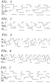
- a representative divided down clock reference signal output from divide by N counter 14 is shown in FIG. 3 as signal f B .
- a representative divided down desired clock signal output from divide by M counter 24 is shown in FIG. 3 as signal f A .
- Signals f A and f B have the same frequency.
- Signal f AQUAD is signal f A phase delayed by 90° by phase generator circuit 26.
- Signal OUT represents the output from the shift register and, with these inputs to the shift register, is a sequence of logic ones.
- Reset 34 detects when the output of shift register 18 does not remain all logic ones, corresponding the frequency generator locking onto a harmonic frequency, and forces the frequency generator to a lower frequency of operation.
- the output from the shift register could also be provided to a harmonic decode circuit (not shown) to determine which harmonic the frequency generator locks onto.
- Harmonic decode circuit 28 decodes the sequence of logic ones to indicate the phase-locked loop has locked onto the desired clock signal frequency. When each output from the shift register is repetitive of the previous states, the phase-locked loop has locked onto the desired clock signal frequency. In the preferred embodiment, the sequence of logic ones provides the sufficient condition to be certain that the phase-locked loop has locked onto the desired clock signal frequency. Since the phase-locked loop locked onto the desired clock signal frequency, no oscillator control action is initiated based on the output from shift register 18.
- the second harmonic of signal f A is represented in FIG. 4.
- the second harmonic, designated 2xf A by definition is twice the frequency of signal f A .
- the rising leading edge of every other cycle of the second harmonic occurs concurrently with the rising leading edge of the desired clock signal.
- the concurrent occurrence of this characteristic permits the phase-locked loop to harmonically lock.
- the phase generator circuit would produce a phase delayed signal, such as signal 2xf A QUAD , at the same frequency as the second harmonic but phase shifted therefrom, preferably 90°.
- the shift register provides an output, OUT, shown in FIG. 4 that is a repetitive sequence of logic states, 101010.
- Harmonic decode circuit 28 decodes the sequence of logic states. Circuit 28 detects that the sequence of logic states output from the shift register repeats each two logic states, indicating the phase-locked loop has harmonically locked onto the second harmonic. Alternatively, in a digital oscillator control, a register may be reset to a low state to force the oscillator control to shift operation of the oscillator to another frequency and allow operation of the phase-locked loop to hopefully settle in on and lock to the desired clock signal frequency. In an analog control, the voltage would be lowered to force the phase-locked loop out of harmonic lock to a lower frequency of operation.
- the third and fourth harmonics of signal f A are shown in FIGs. 5 and 6, respectively.
- the third ( 3xf A ) and fourth ( 4xf A ) harmonic signals have rising leading edges, every third and fourth cycle, respectively, that occur concurrently with the rising leading edge of the divided down oscillator clock signal.
- Shown with the third harmonic in FIG. 5 is a 90° phase shifted third harmonic 3xf A QUAD and the output, OUT.
- the output OUT of the shift register would be a repetitive sequence of 110110 which could be used to take direct oscillator control action as described above.
- Circuit 28 detects that the sequence of logic states output from the shift register repeats each three logic states, indicating the phase-locked loop has harmonically locked onto the third harmonic.
- Shown with the fourth harmonic in FIG. 6 is a 90° phase shifted fourth harmonic 4xf AQUAD and the output, OUT. If the fourth harmonic is generated by the clock generation circuit 12 and the phase-locked loop harmonically locks into the fourth harmonic, the output, OUT, of the shift register would be a repetitive sequence of 11001100 which could be used to take direct oscillator control action as described above, or could be decoded by harmonic decode circuit 28. Circuit 28 detects that the sequence of logic states output from the shift register repeats each four logic states, indicating the phase-locked loop has harmonically locked onto the fourth harmonic.
- FIG. 7 illustrates that the phase of signal f A need not be the quadrature phase for the harmonic lock detector circuit to detect harmonic locking.
- Signals f A and f B from FIG. 3 are repeated.
- a phase shifted f A PHASE having the same frequency as signal f A , phase delayed by approximately 60° is shown.
- the output is a sequence of logic ones indicating that the phase-locked loop has locked onto the desired clock signal frequency. It can be observed from FIGs.
- phase-locked loop harmonic lock detector circuit in silicon.
Landscapes
- Stabilization Of Oscillater, Synchronisation, Frequency Synthesizers (AREA)
Applications Claiming Priority (2)
| Application Number | Priority Date | Filing Date | Title |
|---|---|---|---|
| US982817 | 1992-11-30 | ||
| US07/982,817 US5337022A (en) | 1992-11-30 | 1992-11-30 | Harmonic lock detector |
Publications (3)
| Publication Number | Publication Date |
|---|---|
| EP0600680A2 true EP0600680A2 (fr) | 1994-06-08 |
| EP0600680A3 EP0600680A3 (fr) | 1995-01-04 |
| EP0600680B1 EP0600680B1 (fr) | 1999-03-17 |
Family
ID=25529535
Family Applications (1)
| Application Number | Title | Priority Date | Filing Date |
|---|---|---|---|
| EP93309462A Expired - Lifetime EP0600680B1 (fr) | 1992-11-30 | 1993-11-26 | Détecteur de verrouillage sur une fréquence harmonique |
Country Status (5)
| Country | Link |
|---|---|
| US (1) | US5337022A (fr) |
| EP (1) | EP0600680B1 (fr) |
| JP (1) | JPH06224755A (fr) |
| KR (1) | KR940012826A (fr) |
| DE (1) | DE69323964T2 (fr) |
Families Citing this family (13)
| Publication number | Priority date | Publication date | Assignee | Title |
|---|---|---|---|---|
| US5675273A (en) * | 1995-09-08 | 1997-10-07 | International Business Machines Corporation | Clock regulator with precision midcycle edge timing |
| US5909130A (en) * | 1996-04-30 | 1999-06-01 | Lucent Technologies Inc. | Digital lock detector for phase-locked loop |
| US5627496A (en) * | 1996-06-17 | 1997-05-06 | Lucent Technologies Inc. | PLL and phase detection circuit therefor |
| US5926052A (en) * | 1996-07-01 | 1999-07-20 | Motorola, Inc. | Variable phase shifter and method |
| NL1021440C2 (nl) * | 2001-09-28 | 2004-07-15 | Samsung Electronics Co Ltd | Vertragingsvergrendelde lus met meervoudige fasen. |
| US7091762B2 (en) * | 2001-10-09 | 2006-08-15 | Gallitzin Allegheny Llc | Systems and methods for minimizing harmonic interference |
| US7209533B1 (en) * | 2003-05-13 | 2007-04-24 | National Semiconductor Corporation | Delay locked loop with harmonic lock and hang prevention architecture |
| TWI345382B (en) * | 2008-03-27 | 2011-07-11 | Novatek Microelectronics Corp | Phase lock loop (pll) system and phase locking method for pll |
| US7786763B1 (en) | 2008-12-30 | 2010-08-31 | Integrated Device Technology, Inc. | Clock circuit with harmonic frequency detector |
| US8786374B2 (en) | 2012-07-17 | 2014-07-22 | Freescale Semiconductor, Inc. | Error detection at an oscillator |
| KR102053352B1 (ko) * | 2013-02-25 | 2019-12-09 | 삼성전자주식회사 | 고조파 락을 방지할 수 있는 위상 동기 루프 및 이를 포함하는 장치들 |
| US9252788B1 (en) | 2014-09-11 | 2016-02-02 | International Business Machines Corporation | Phase error detection in phase lock loop and delay lock loop devices |
| KR102375952B1 (ko) | 2015-01-22 | 2022-03-17 | 삼성전자주식회사 | 위상 고정 검출 장치 및 검출 방법 |
Family Cites Families (6)
| Publication number | Priority date | Publication date | Assignee | Title |
|---|---|---|---|---|
| US3988696A (en) * | 1975-11-28 | 1976-10-26 | The Bendix Corporation | Phase lock detector for digital frequency synthesizer |
| US4077016A (en) * | 1977-02-22 | 1978-02-28 | Ncr Corporation | Apparatus and method for inhibiting false locking of a phase-locked loop |
| US4115745A (en) * | 1977-10-04 | 1978-09-19 | Gte Sylvania Incorporated | Phase lock speed-up circuit |
| US4151463A (en) * | 1978-02-02 | 1979-04-24 | Bell Telephone Laboratories, Incorporated | Phase locked loop indicator |
| DE2918850C2 (de) * | 1979-05-10 | 1983-05-26 | Licentia Patent-Verwaltungs-Gmbh, 6000 Frankfurt | Verfahren und Schaltungsanordnung zum Erkennen des Regelzustandes einer Phasenregelschleife |
| US4590440A (en) * | 1984-07-06 | 1986-05-20 | American Microsystems, Inc. | Phase locked loop with high and/or low frequency limit detectors for preventing false lock on harmonics |
-
1992
- 1992-11-30 US US07/982,817 patent/US5337022A/en not_active Expired - Lifetime
-
1993
- 1993-11-26 EP EP93309462A patent/EP0600680B1/fr not_active Expired - Lifetime
- 1993-11-26 DE DE69323964T patent/DE69323964T2/de not_active Expired - Fee Related
- 1993-11-29 KR KR1019930025670A patent/KR940012826A/ko not_active Withdrawn
- 1993-11-30 JP JP5298759A patent/JPH06224755A/ja not_active Withdrawn
Also Published As
| Publication number | Publication date |
|---|---|
| EP0600680A3 (fr) | 1995-01-04 |
| DE69323964T2 (de) | 1999-08-19 |
| KR940012826A (ko) | 1994-06-24 |
| JPH06224755A (ja) | 1994-08-12 |
| EP0600680B1 (fr) | 1999-03-17 |
| DE69323964D1 (de) | 1999-04-22 |
| US5337022A (en) | 1994-08-09 |
Similar Documents
| Publication | Publication Date | Title |
|---|---|---|
| US6407642B2 (en) | Frequency detector and phase-locked loop circuit including the detector | |
| US5302916A (en) | Wide range digital frequency detector | |
| US5337022A (en) | Harmonic lock detector | |
| EP0637138A1 (fr) | Circuit de détection de synchronisation | |
| US6441667B1 (en) | Multiphase clock generator | |
| US6222420B1 (en) | Minimizing recovery time | |
| US5159279A (en) | Apparatus and method for detecting out-of-lock condition in a phase lock loop | |
| US7218157B2 (en) | Phase locked loop | |
| KR0138220B1 (ko) | 위상동기루프회로의 클럭지연보상 및 듀티제어 장치 | |
| EP0041561A1 (fr) | Circuit de boucles a verrouillage de phases stabilise par un oscillateur a quartz | |
| US6757349B1 (en) | PLL frequency synthesizer with lock detection circuit | |
| US5506531A (en) | Phase locked loop circuit providing increase locking operation speed using an unlock detector | |
| US6990165B2 (en) | Phase and frequency lock detector | |
| KR100652390B1 (ko) | 데드락 방지회로를 구비하는 위상동기 루프 회로 및 이의데드락 방지방법 | |
| US5153725A (en) | Automatic frequency control circuit | |
| US6249560B1 (en) | PLL circuit and noise reduction means for PLL circuit | |
| US4801894A (en) | Frequency detector for frequency locked loop | |
| JP2877185B2 (ja) | クロック発生器 | |
| US7123100B2 (en) | Divider circuit and oscillating circuit including the same | |
| JPH03216025A (ja) | 並列直列変換器 | |
| JP2736702B2 (ja) | 非同期検出回路 | |
| JPH0795051A (ja) | ディジタルpll回路 | |
| JPS58130630A (ja) | Pll回路 | |
| KR20010084067A (ko) | 원샷 딜레이 회로를 구비한 디지털 락 검출 회로 | |
| JPH10233681A (ja) | Pll回路 |
Legal Events
| Date | Code | Title | Description |
|---|---|---|---|
| PUAI | Public reference made under article 153(3) epc to a published international application that has entered the european phase |
Free format text: ORIGINAL CODE: 0009012 |
|
| AK | Designated contracting states |
Kind code of ref document: A2 Designated state(s): DE ES FR GB IT |
|
| RAP3 | Party data changed (applicant data changed or rights of an application transferred) |
Owner name: AT&T CORP. |
|
| PUAL | Search report despatched |
Free format text: ORIGINAL CODE: 0009013 |
|
| AK | Designated contracting states |
Kind code of ref document: A3 Designated state(s): DE ES FR GB IT |
|
| 17P | Request for examination filed |
Effective date: 19950622 |
|
| 17Q | First examination report despatched |
Effective date: 19960920 |
|
| GRAG | Despatch of communication of intention to grant |
Free format text: ORIGINAL CODE: EPIDOS AGRA |
|
| GRAG | Despatch of communication of intention to grant |
Free format text: ORIGINAL CODE: EPIDOS AGRA |
|
| GRAH | Despatch of communication of intention to grant a patent |
Free format text: ORIGINAL CODE: EPIDOS IGRA |
|
| GRAH | Despatch of communication of intention to grant a patent |
Free format text: ORIGINAL CODE: EPIDOS IGRA |
|
| GRAA | (expected) grant |
Free format text: ORIGINAL CODE: 0009210 |
|
| AK | Designated contracting states |
Kind code of ref document: B1 Designated state(s): DE ES FR GB IT |
|
| PG25 | Lapsed in a contracting state [announced via postgrant information from national office to epo] |
Ref country code: IT Free format text: LAPSE BECAUSE OF FAILURE TO SUBMIT A TRANSLATION OF THE DESCRIPTION OR TO PAY THE FEE WITHIN THE PRE;WARNING: LAPSES OF ITALIAN PATENTS WITH EFFECTIVE DATE BEFORE 2007 MAY HAVE OCCURRED AT ANY TIME BEFORE 2007. THE CORRECT EFFECTIVE DATE MAY BE DIFFERENT FROM THE ONE RECORDED.SCRIBED TIME-LIMIT Effective date: 19990317 Ref country code: ES Free format text: THE PATENT HAS BEEN ANNULLED BY A DECISION OF A NATIONAL AUTHORITY Effective date: 19990317 |
|
| REF | Corresponds to: |
Ref document number: 69323964 Country of ref document: DE Date of ref document: 19990422 |
|
| ET | Fr: translation filed | ||
| PLBE | No opposition filed within time limit |
Free format text: ORIGINAL CODE: 0009261 |
|
| 26N | No opposition filed | ||
| PGFP | Annual fee paid to national office [announced via postgrant information from national office to epo] |
Ref country code: FR Payment date: 20001025 Year of fee payment: 8 |
|
| PGFP | Annual fee paid to national office [announced via postgrant information from national office to epo] |
Ref country code: GB Payment date: 20001026 Year of fee payment: 8 |
|
| PGFP | Annual fee paid to national office [announced via postgrant information from national office to epo] |
Ref country code: DE Payment date: 20001229 Year of fee payment: 8 |
|
| PG25 | Lapsed in a contracting state [announced via postgrant information from national office to epo] |
Ref country code: GB Free format text: LAPSE BECAUSE OF NON-PAYMENT OF DUE FEES Effective date: 20011126 |
|
| REG | Reference to a national code |
Ref country code: GB Ref legal event code: IF02 |
|
| PG25 | Lapsed in a contracting state [announced via postgrant information from national office to epo] |
Ref country code: DE Free format text: LAPSE BECAUSE OF NON-PAYMENT OF DUE FEES Effective date: 20020702 |
|
| GBPC | Gb: european patent ceased through non-payment of renewal fee |
Effective date: 20011126 |
|
| PG25 | Lapsed in a contracting state [announced via postgrant information from national office to epo] |
Ref country code: FR Free format text: LAPSE BECAUSE OF NON-PAYMENT OF DUE FEES Effective date: 20020730 |
|
| REG | Reference to a national code |
Ref country code: FR Ref legal event code: ST |
|
| REG | Reference to a national code |
Ref country code: FR Ref legal event code: ST |