EP0600802A1 - RF Generator mit variabler und gesteuerter Ausgangsleistung - Google Patents
RF Generator mit variabler und gesteuerter Ausgangsleistung Download PDFInfo
- Publication number
- EP0600802A1 EP0600802A1 EP93402933A EP93402933A EP0600802A1 EP 0600802 A1 EP0600802 A1 EP 0600802A1 EP 93402933 A EP93402933 A EP 93402933A EP 93402933 A EP93402933 A EP 93402933A EP 0600802 A1 EP0600802 A1 EP 0600802A1
- Authority
- EP
- European Patent Office
- Prior art keywords
- output
- input
- amplifier
- output signal
- power
- Prior art date
- Legal status (The legal status is an assumption and is not a legal conclusion. Google has not performed a legal analysis and makes no representation as to the accuracy of the status listed.)
- Ceased
Links
- 230000001105 regulatory effect Effects 0.000 title description 2
- 238000001514 detection method Methods 0.000 claims description 7
- 230000005284 excitation Effects 0.000 claims description 6
- 238000010586 diagram Methods 0.000 description 4
- 101100115778 Caenorhabditis elegans dac-1 gene Proteins 0.000 description 1
- 230000006978 adaptation Effects 0.000 description 1
- 230000017105 transposition Effects 0.000 description 1
Images

Classifications
-
- H—ELECTRICITY
- H03—ELECTRONIC CIRCUITRY
- H03G—CONTROL OF AMPLIFICATION
- H03G3/00—Gain control in amplifiers or frequency changers
- H03G3/20—Automatic control
- H03G3/30—Automatic control in amplifiers having semiconductor devices
- H03G3/3036—Automatic control in amplifiers having semiconductor devices in high-frequency amplifiers or in frequency-changers
- H03G3/3042—Automatic control in amplifiers having semiconductor devices in high-frequency amplifiers or in frequency-changers in modulators, frequency-changers, transmitters or power amplifiers
-
- H—ELECTRICITY
- H03—ELECTRONIC CIRCUITRY
- H03L—AUTOMATIC CONTROL, STARTING, SYNCHRONISATION OR STABILISATION OF GENERATORS OF ELECTRONIC OSCILLATIONS OR PULSES
- H03L5/00—Automatic control of voltage, current, or power
- H03L5/02—Automatic control of voltage, current, or power of power
Definitions
- the present invention relates to a radiofrequency wave generator with variable and regulated output power using a regulation loop to regulate the output power signal around a set value supplied by means of a digital-analog converter, hereinafter designated as CNA, and control the power level of the generator output signal.
- CNA digital-analog converter
- a control loop takes a fraction of the generator output signal which, after detection by a device of the diode detector type, is compared to a table of set point voltages each corresponding to a predetermined attenuation value of the output signal.
- the regulation around the predetermined setpoint is carried out by comparison of the signal detected by the detection device with the setpoint signal before the attenuation command.
- the fraction of the detected output signal varies exponentially depending on the dynamics of the power of the generator output signal while the analog output voltage of the DAC varies linearly according to a number of steps, the maximum number of which is determined. to cover the entire dynamic range of the output signal power. This results in a significant variation in the precision of the attenuation setting, particularly for low power levels of the output signal. Given the exponential variation of the detected signal proportional to the power of the output signal, the accuracy of the attenuation setting is less good for low power values corresponding to the start of power dynamics than for power values corresponding to the end of the dynamics.
- a first known solution consists in obtaining a reference voltage which varies in the same way as the detected voltage to be compared.
- an amplifier anti-logarithmic is placed for example at the output of the DAC.
- a second solution consists, for example, in placing a logarithmic amplifier after the device for detecting the regulation loop.
- the two main solutions have the main drawback of requiring a complex use of logarithmic or anti-logarithmic amplifiers, which are particularly energy-consuming in development time.
- the invention aims to overcome the aforementioned drawback.
- the subject of the invention is a radio frequency wave generator comprising a main circuit comprising at least one device delivering an excitation signal, an attenuator controlled by a control voltage, a device for processing the excitation signal and comprising a regulation loop comprising a detector delivering a detection voltage the variation of which is of exponential form proportional to the power of the generator output signal and a comparator comparing the detected voltage with a reference voltage delivered by a control device of the attenuator, characterized in that the control device, organized around a ground circuit serving as reference potential, comprises a digital-analog converter receiving on a first input digital information each corresponding to a determined attenuation value of the power of the output signal and receiving on a second me input a variable reference current which is a function of the attenuation value selected on the converter and determined to cover all the dynamics of the power of the output signal, and whose output is coupled to the input of an amplifier, a feedback resistance of the amplifier being coupled between the input and the output of the amplifier which is also loope
- the main advantage of the device according to the invention is that it makes it possible to improve the precision of adjusting the attenuation of the power level of the output signal for low power levels by varying the current almost exponentially. of reference defining the step of the CNA with a simplified implementation.
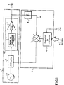
- FIG. 1 illustrates a simplified block diagram of a radiofrequency generator comprising a main circuit 1, represented inside a discontinuous closed line, and comprising, from the input to the output, a device 2 d excitation delivering for example an intermediate frequency signal, Fl, of 1.4 MHz modulated by a low frequency signal, the output of which is coupled to a first input of a controlled attenuator 3.
- the output of the attenuator 3 is coupled to a processing device 4 represented inside a continuous closed line comprising, for example a frequency transposition chain 5 coupled to an output amplifier 6 delivering on its output a radiofrequency signal S.
- a loop 7 represented at l inside a discontinuous closed line takes a fraction of the power P S of the signal S which is injected at the input of a detection device 8, for example with diodes, whose output delivering a voltage V d is coupled to a first positive operand input of a comparator 9.
- a second input d negative operand of comparator 9 receives an analog reference signal, for example a voltage V c , coming from a control device 10 of the attenuator 3 receiving on a first input a reference voltage V ref and on a second input a digital data bus each corresponding to a predetermined attenuation value.
- the signal from the comparison is injected at a second input of the attenuator 3.
- FIG. 2 An electrical diagram of an embodiment of the control device 10 is illustrated in FIG. 2.
- the control device 10, represented inside a continuous line, is organized around a reference potential, for example , a ground potential M. II comprises from the input to the output, a first resistor R1 receiving on one of its terminals the reference voltage V ref , the other terminal being coupled to a first input of a DAC 11 receiving on a second input a digital data bus.
- the output of the DAC 11 is coupled to the input of an amplifier 12 with fixed gain, for example equal to one, serving as an adaptation stage at the output of the control device 10.
- a resistor R3 determining the gain of the amplifier 12 is coupled between the output and input of amplifier 12.
- the output of amplifier 12 is also looped back to the input of the DAC 1 1 which also corresponds to one of the terminals of the first resistor R1, by a loop 13, shown inside a broken line.
- the loop 13 includes a resistor R2 and an optional diode D, shown in broken lines, which can be coupled between the resistor R2 and the first input of the DAC.
- the three resistors R1, R2 and R3 of the control device 10 enable the reference current I ref entering the first input of the DAC 11 to be determined and condition the almost exponential of the setpoint voltage V c at the output of amplifier 12.
- the output signal, or setpoint voltage, V c delivered by the control device 10 is then injected onto the negative operand input of the comparator 9.
- Each binary item of information brought by the bus is converted, for example from a table of predetermined values, into an analog reference voltage V c to the exit of the CNA.
- a digital application is given below by way of example.
- the dynamic range of the power P S of the output signal S is 30 dB.
- the attenuation step is chosen equal to 3 dB with precision on each attenuation step better than 0.5 dB. To cover this 30 dB dynamic range, an eight-bit coded DAC is used.
- the attenuation values N therefore vary from: 1 256 ⁇ N ⁇ 255 256
- the diode D is not essential for the operation of the generator according to the invention nevertheless it helps in the determination of the values of the resistances R1 and R3 of the control device 10 in the operating zone where the diode D is blocked, that is to say i.e. for the setpoint voltage V c values lower than the diode detection threshold voltage.D
- the loop 13 of the control device 10 is not activated.
- the characteristic V c as a function of the attenuation values N is then reduced to a straight line whose slope is a function of the value of the resistances R1 and R3 to obtain sufficient precision in dB by step of attenuation at the bottom of the characteristic V c function of N.
- the loop 13 is activated and the shape of the characteristic then becomes almost exponential, as illustrated in FIG. 3a, with a starting slope identical to the slope given by the control device 10, the loop 13 being deactivated.
- the characteristic then follows as closely as possible the variation of the detected voltage V d as a function of the dynamics of the power P S of the output signal S.
Landscapes
- Control Of Amplification And Gain Control (AREA)
Applications Claiming Priority (2)
| Application Number | Priority Date | Filing Date | Title |
|---|---|---|---|
| FR9214639A FR2699020B1 (fr) | 1992-12-04 | 1992-12-04 | Générateur d'ondes radiofréquences à puissance de sortie variable et régulée. |
| FR9214639 | 1992-12-04 |
Publications (1)
| Publication Number | Publication Date |
|---|---|
| EP0600802A1 true EP0600802A1 (de) | 1994-06-08 |
Family
ID=9436242
Family Applications (1)
| Application Number | Title | Priority Date | Filing Date |
|---|---|---|---|
| EP93402933A Ceased EP0600802A1 (de) | 1992-12-04 | 1993-12-03 | RF Generator mit variabler und gesteuerter Ausgangsleistung |
Country Status (2)
| Country | Link |
|---|---|
| EP (1) | EP0600802A1 (de) |
| FR (1) | FR2699020B1 (de) |
Citations (3)
| Publication number | Priority date | Publication date | Assignee | Title |
|---|---|---|---|---|
| DE3236148A1 (de) * | 1982-09-29 | 1984-03-29 | Siemens AG, 1000 Berlin und 8000 München | Schaltungsanordnung zum einstellen der verstaerkung eines verstaerkers |
| DE3433901A1 (de) * | 1984-09-14 | 1986-03-27 | Siemens AG, 1000 Berlin und 8000 München | Schaltung zur leistungssteuerung von hochfrequenzsendern |
| EP0414352A2 (de) * | 1989-06-26 | 1991-02-27 | ORBITEL MOBILE COMMUNICATIONS LIMITED (Reg. no. 2515004) | Funksender mit Ausgangsleistungssteuerung |
-
1992
- 1992-12-04 FR FR9214639A patent/FR2699020B1/fr not_active Expired - Fee Related
-
1993
- 1993-12-03 EP EP93402933A patent/EP0600802A1/de not_active Ceased
Patent Citations (3)
| Publication number | Priority date | Publication date | Assignee | Title |
|---|---|---|---|---|
| DE3236148A1 (de) * | 1982-09-29 | 1984-03-29 | Siemens AG, 1000 Berlin und 8000 München | Schaltungsanordnung zum einstellen der verstaerkung eines verstaerkers |
| DE3433901A1 (de) * | 1984-09-14 | 1986-03-27 | Siemens AG, 1000 Berlin und 8000 München | Schaltung zur leistungssteuerung von hochfrequenzsendern |
| EP0414352A2 (de) * | 1989-06-26 | 1991-02-27 | ORBITEL MOBILE COMMUNICATIONS LIMITED (Reg. no. 2515004) | Funksender mit Ausgangsleistungssteuerung |
Non-Patent Citations (1)
| Title |
|---|
| R. F. WOLFFENBUTTEL: "digitally programmable accurate current sources for logarithmic control of the amplification or attenuation in a gain cell.", IEEE JOURNAL OF SOLID-STATE CIRCUITS, vol. 23, no. 3, June 1988 (1988-06-01), NEW YORK US, pages 767 - 773, XP001093045, DOI: doi:10.1109/4.317 * |
Also Published As
| Publication number | Publication date |
|---|---|
| FR2699020A1 (fr) | 1994-06-10 |
| FR2699020B1 (fr) | 1995-01-06 |
Similar Documents
| Publication | Publication Date | Title |
|---|---|---|
| EP0583186B1 (de) | Vorrichtung zur Leistungsstabilisierung von Laserdioden | |
| EP0034957B1 (de) | Vorrichtung zur automatischen Regulierung der Ausgangsleistung eines Sendermoduls für ein Übertragungssystem mit optischen Fasern | |
| EP0052536B1 (de) | Sendermodul-Ausgangsleistungsstabilisierungsanordnung für ein Lichtwellenleiter-Übertragungssystem | |
| FR2662557A1 (fr) | Convertisseur basse tension-haute tension. | |
| EP0632585A1 (de) | Vorrichtung zur Steuerung der Vorspannung eines Verstärkers | |
| EP0278193B1 (de) | Schaltung zum Messen des die Primärwicklung des Ausgangstransformators eines Wechselrichters durch fliessenden Gleichstromanteiles | |
| EP0567380B1 (de) | Verfahren und Vorrichtung zur Kompensation von Phasenschwankungen von einer mit einem Hochfrequenzrohr verstärkten Welle | |
| EP0011534B1 (de) | Verfahren und Vorrichtung zur Verarbeitung von analogischen, insbesondere pseudoperiodischen Signalen | |
| EP0809342A1 (de) | Anordnung zur Regelung der Ladung einer modularen Einheit von elektrochemischen Zellen, die in Reihe geschaltet sind und entsprechendes Modul zur Messung der Zellen | |
| EP0065901A1 (de) | Potentiometermesswertumformersystem | |
| EP0600802A1 (de) | RF Generator mit variabler und gesteuerter Ausgangsleistung | |
| FR2712751A1 (fr) | Procédé et dispositif de régulation du gain d'un amplificateur de signaux haute fréquence. | |
| EP0106728A1 (de) | Verfahren und Vorrichtung zur Verstärkungsstabilisierung eines fotoempfindlichen Avalanche-Bauelements | |
| EP1085624A1 (de) | Verfahren und Vorrichtung zur optischen Leistungsstabilisierung eines Lasers | |
| FR2467407A1 (fr) | Dispositif de mesure des valeurs cretes d'un phenomene non periodique a recurrence faible | |
| EP0308293B1 (de) | Steuerung der Ausgangsleistung eines Klasse-C-Verstärkers | |
| EP0530072B1 (de) | Verfahren und Vorrichtung zur Steuerung und Regelung | |
| EP0678751B1 (de) | Detektorvorrichtung für Änderungen einer Versorgungsspannung | |
| FR2721715A1 (fr) | Dispositif de mesure de l'état de charge d'un générateur électrochimique. | |
| EP0050583B1 (de) | Wechselspannung/Gleichstrom-Konverter und Schwingkreis-Schaltung mit einem solchen Konverter | |
| EP0159263A1 (de) | Verfahren und Vorrichtung zur Kontrolle des Flüssigkeitsstandes in einem Tank | |
| EP0047683A1 (de) | Einrichtung zur Fehlererkennung eines ternären Signals | |
| EP0851563B1 (de) | Schaltnetzteileinrichtung mit kontrollierter elektromagnetischer Störung | |
| EP0063516B1 (de) | Verfahren zum Messen von Verstärkungsänderungen in einem Laserverstärker und Vorrichtung zur Durchführung des Verfahrens | |
| EP0838901B1 (de) | Analog-Digital-Wandlungsgerät mit geregelter Eingangsdynamik |
Legal Events
| Date | Code | Title | Description |
|---|---|---|---|
| PUAI | Public reference made under article 153(3) epc to a published international application that has entered the european phase |
Free format text: ORIGINAL CODE: 0009012 |
|
| AK | Designated contracting states |
Kind code of ref document: A1 Designated state(s): DE GB IT |
|
| 17P | Request for examination filed |
Effective date: 19941126 |
|
| GRAG | Despatch of communication of intention to grant |
Free format text: ORIGINAL CODE: EPIDOS AGRA |
|
| 17Q | First examination report despatched |
Effective date: 19970117 |
|
| STAA | Information on the status of an ep patent application or granted ep patent |
Free format text: STATUS: THE APPLICATION HAS BEEN REFUSED |
|
| 18R | Application refused |
Effective date: 19970821 |