EP0601650A1 - Affichage matriciel réparable - Google Patents
Affichage matriciel réparable Download PDFInfo
- Publication number
- EP0601650A1 EP0601650A1 EP93203396A EP93203396A EP0601650A1 EP 0601650 A1 EP0601650 A1 EP 0601650A1 EP 93203396 A EP93203396 A EP 93203396A EP 93203396 A EP93203396 A EP 93203396A EP 0601650 A1 EP0601650 A1 EP 0601650A1
- Authority
- EP
- European Patent Office
- Prior art keywords
- row
- stages
- shift register
- conductors
- address conductors
- Prior art date
- Legal status (The legal status is an assumption and is not a legal conclusion. Google has not performed a legal analysis and makes no representation as to the accuracy of the status listed.)
- Withdrawn
Links
Images

Classifications
-
- G—PHYSICS
- G11—INFORMATION STORAGE
- G11C—STATIC STORES
- G11C29/00—Checking stores for correct operation ; Subsequent repair; Testing stores during standby or offline operation
- G11C29/70—Masking faults in memories by using spares or by reconfiguring
- G11C29/86—Masking faults in memories by using spares or by reconfiguring in serial access memories, e.g. shift registers, CCDs, bubble memories
-
- G—PHYSICS
- G09—EDUCATION; CRYPTOGRAPHY; DISPLAY; ADVERTISING; SEALS
- G09G—ARRANGEMENTS OR CIRCUITS FOR CONTROL OF INDICATING DEVICES USING STATIC MEANS TO PRESENT VARIABLE INFORMATION
- G09G3/00—Control arrangements or circuits, of interest only in connection with visual indicators other than cathode-ray tubes
- G09G3/20—Control arrangements or circuits, of interest only in connection with visual indicators other than cathode-ray tubes for presentation of an assembly of a number of characters, e.g. a page, by composing the assembly by combination of individual elements arranged in a matrix no fixed position being assigned to or needed to be assigned to the individual characters or partial characters
- G09G3/34—Control arrangements or circuits, of interest only in connection with visual indicators other than cathode-ray tubes for presentation of an assembly of a number of characters, e.g. a page, by composing the assembly by combination of individual elements arranged in a matrix no fixed position being assigned to or needed to be assigned to the individual characters or partial characters by control of light from an independent source
- G09G3/36—Control arrangements or circuits, of interest only in connection with visual indicators other than cathode-ray tubes for presentation of an assembly of a number of characters, e.g. a page, by composing the assembly by combination of individual elements arranged in a matrix no fixed position being assigned to or needed to be assigned to the individual characters or partial characters by control of light from an independent source using liquid crystals
- G09G3/3611—Control of matrices with row and column drivers
- G09G3/3674—Details of drivers for scan electrodes
- G09G3/3677—Details of drivers for scan electrodes suitable for active matrices only
-
- G—PHYSICS
- G09—EDUCATION; CRYPTOGRAPHY; DISPLAY; ADVERTISING; SEALS
- G09G—ARRANGEMENTS OR CIRCUITS FOR CONTROL OF INDICATING DEVICES USING STATIC MEANS TO PRESENT VARIABLE INFORMATION
- G09G2330/00—Aspects of power supply; Aspects of display protection and defect management
- G09G2330/08—Fault-tolerant or redundant circuits, or circuits in which repair of defects is prepared
Definitions
- a matrix display apparatus comprising a multiplicity of pixels, an array of row and column address conductors which are insulated from each other and which are electrically coupled to ones of the pixels which are spatially associated with places where said row and column address conductors cross each other, and means for addressing the row and column address conductors to enable selective application to the pixels of respective signals representative of an image to be presented by the apparatus.
- LCD liquid crystal display
- TFTs thin-film transistors
- the pixels and their associated TFTs are located at places where transversely-arranged row and column address conductors cross, and specific pixels are selected by addressing the respective intersecting row and column address conductors.
- LCD structure and of circuitry for addressing TFT-activated pixels one may refer to texts such as E. Kaneko, Liquid Crystal TV Displays, D. Reidel Publishing Company, Kluwer Academic Publishers Group, 1987.
- Figure 1 illustrates a known liquid crystal display apparatus which includes redundant row-addressing circuitry.
- the display apparatus includes a multiplicity of pixels (and their associated TFTs) which are each identified by a respective designation P m,n , where m and n identify the specific row and column address conductors over which each pixel is addressed.
- the row and column address conductors are designated LR1, LR2, ... LR M and LC1, LC2, LC3, ... LC N , respectively.
- the redundant row-addressing circuitry includes duplicate circuits 10 and 10', each of which has an input for receiving row clock pulses, an input for receiving periodic start pulses, and a multiplicity of outputs electrically connected to respective row address conductors.
- the display apparatus also includes a column-addressing circuit 12 having a first input for receiving column timing pulses, a second input for receiving an image signal, and a multiplicity of outputs electrically connected to respective column address conductors.
- a typical use for a LCD apparatus is projecting or directly displaying a television image.
- the image signal is derived from the video signal, while the column timing pulses, the row clock pulses, and the start pulses are derived from the vertical and horizontal synch pulses.
- the image signal has a time-varying voltage which is to be continually sampled and applied over the column address conductors to sequentially-addressed pixels of the display.
- a line of video information is stored in a line memory to enable simultaneous (parallel) addressing of the column address conductors.
- Row-addressing circuit 10 includes an M-stage shift register, having stages S1, S2, ... S M , and M output buffer devices B1, B2, ... B M electrically connected in openings in the row address conductors LR1, LR2, ... LR M to couple the outputs of respective shift register stages to the pixels.
- the output of each stage S m is electrically connected to the input of a successive stage S m+1 so that a logical ONE can be continually propagated through the shift register under the control of the row-clock pulses.
- the logical ONE propagates through the shift register, it appears successively at the inputs of the buffer devices B1, B2, ... B M and successively addresses the rows of pixels located along the respective row address conductors. More precisely, as the voltage level corresponding to a logical ONE appears at the output of each shift register stage, it causes the connected buffer device to produce a predetermined output voltage which will switch ON the TFTs associated with the pixels in the selected row.
- Column-addressing circuit 12 functions similarly to row-addressing circuit 10. However, in addition to addressing the column address conductors LC1, LC2, ... LC N , it supplies to these conductors data signals representative of samples of the image signal. Specifically, while any row of pixels is addressed by circuit 10, the column-addressing circuit applies to the column address conductors for these pixels, data signals representative of brightnesses, e.g. gray levels, corresponding to the segments of the image to be displayed by these pixels.
- a specific column-addressing circuit will not be described, because it is not needed for an understanding of the invention. Many varieties of such data-supplying, column-addressing circuits are known.
- Row-addressing circuit 10' is a duplicate of row-addressing circuit 10 and receives the same row clock signal. This duplicate circuit is provided to ensure that each row address conductor is addressed at the appropriate time, even if row-addressing circuit 10 has a defect which prevents it from addressing one or more row address conductors. Ideally, the duplicate row-addressing circuit would provide complete redundancy, so that there will be no deterioration of the image displayed by the pixels even if row-addressing circuit 10 fails completely. Unfortunately, however, this is often not the result.
- the duplicate circuit has a defect in its shift register stage S4' which similarly stops the propagation of the logical ONE in the duplicate shift register, the last addressable row of pixels in the display will be those in row 3. All subsequent rows of pixels will be inoperable.
- the second general category of defects which cannot be cured by the duplicate row-addressing circuit relates to buffer devices which become locked in a low-output-impedance mode. This can happen, for example, to any buffer device which has a CMOS output inverter. It can be caused by a defect in the device itself or in a shift register stage to which its input is electrically connected.
- the low impedance will provide a path from the row address conductor connected to the output of the buffer device to one of the supply voltages for the buffer device. This could load down the output of the buffer device at the opposite end of the respective row address conductor and make some or all of the pixels in the row inoperable.
- a matrix display apparatus in accordance with the invention is characterized in that the means for addressing the row and column address conductors comprises, at least for a plurality of said address conductors:
- the display apparatus includes openable connection means for selectively disconnecting the outputs of predetermined ones of the stages in the shift register from inputs of successive stages. This permits the output of a defective stage to be isolated from the input of a replacement stage.
- Figure 1 is a schematic diagram of a prior art liquid crystal display with redundant pixel-addressing means.
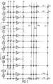
- Figure 2 is a schematic diagram of a preferred embodiment of a row addressing circuit in accordance with the invention.
- Figure 2 illustrates, in part, an exemplary embodiment of a matrix display having a row-addressing circuit in accordance with the invention. Parts in the apparatus which are substantially identical to corresponding parts in the apparatus of Figure 1 are marked identically. For simplicity, the column-addressing circuit 12 is not shown.
- a redundant row-addressing circuit could also be connected to the row address conductors. Most conveniently, this would be done at the opposite end of the row conductors.
- a number of addressing circuits could be provided, with each connected to a different group of conductors. For example, in an interlaced or progressive-scan display, a first row-addressing circuit could be connected to odd-numbered row address conductors and a second row-addressing circuit could be connected to even-numbered row address conductors.
- the row-addressing circuit includes the serially-connected shift register stages S1, S2, ... S N and the buffer devices B1, B2, ... B M which are connected in the row address conductors LR1, LR2, ... LR M , respectively.
- the row-addressing circuit also includes first and second pairs of reparative conductors X1,X2 and X3,X4 which run the length of the shift register, crossing the row address conductors LR1, LR2, ... LR M . These crossing conductors are made electrically connectable to each other by means of closable connection devices.
- Each of the closable connection devices is illustrated by a concentric-circle symbol, which represents first and second conductive pads to which the crossing conductors are separately connected.
- each closable connection device is normally separated from each other by an electrical insulator, but can be electrically connected to each other by wire bonding, by applying conductive paint, or by another technique such as laser fusing.
- the latter technique is particularly applicable if the conductive pads are disposed on opposite sides of an insulating layer and are weldable to each other by focusing a laser beam at the pads and the intervening layer.
- An example of such a welding technique is described in detail in D. E. Castleberry et al., "A 1 Mega-Pixel Color a-Si TFT Liquid Crystal Display", 1988 SID Digest of Technical Papers, pages 232 - 234, paper 13.1.
- a number of spare shift-register stages S x are electrically connected to the pair of reparative conductors X1,X2 at intervals along the length of the shift register.
- Each of these spare shift-register stages has its input connected to conductor X1, has its output connected to conductor X2, and has a control input which is connected to a bus (not shown) that carries the row clock signal.
- a number of spare buffer devices B x are electrically connected to the pair of reparative conductors X3,X4 at intervals along the length of the shift register.
- Each of these spare buffer devices has its input connected to conductor X3 and has its output connected to conductor X4.
- a spare shift register stage element S x and a spare buffer device element B x are provided after every fourth stage of the shift register.
- Many other distributions of these elements are possible, but the probability of being able to repair defects increases with the number of spare stages and buffer devices provided and with their location at strategic positions. For example, if a particular matrix display apparatus is more likely to have defects in specific regions of its addressing circuit(s), the spare elements can be concentrated in these regions rather than evenly distributed along the length of the shift register.
- a plurality of openable connection devices are strategically located in the conductors which connect the successive stages S1, S2, ... S M of the shift register and in the reparative conductors X1,X2,X3,X4.
- Each of these devices which is represented by a wavy-line symbol, is simply a portion of the respective conductor which is disposed in an area of the substrate which facilitates its opening. This could be done, for example, by severing the conductor mechanically, by passing an overcurrent through the portion of the conductor, or by another technique such as vaporizing the portion of the conductor with a laser.
- the openable connection devices could each include a pair of conductive pads between which the portion of conductor to be severed is disposed.
- the defect in stage S3 can be circumvented, making all rows of pixels operable, by opening the connection devices at locations A,B,C and by closing the connection devices at locations D,E.
- the opened connection device at location A will isolate the output of defective shift register stage S3 from successive stages in the shift register and from the input of buffer device B3.
- the closed connection devices at locations D,E will electrically connect the spare shift-register stage S x which is disposed between stages S4 and S5 in place of stage S3.
- the opened connection devices at locations B,C will isolate this spare stage from all other spare stages connected to the reparative conductors X1,X2, so that they can be used independently in the replacement of any stage following stage S5.
- the defect in buffer device B3 can be circumvented by opening the connection devices at locations Q,R,S,T and by closing the connection devices at locations V,W. These opened and closed connections will electrically connect the spare buffer device B x which is disposed between buffer devices B4 and B5 in place of defective buffer device B3, will isolate the defective buffer device from shift-register stage S3 and row address conductor LR3, and will isolate this spare buffer device from all other spare buffer devices connected to the reparative conductors X3,X4. If the input impedance of the defective buffer device remains at a high impedance, it is not necessary to open the connection device at location Q.
- the row-addressing circuit may also include a number of closable connection devices distributed along the length of the reparative conductors.
- One set of such devices is illustrated at locations AA,BB,CC,DD. These devices, which are normally open, facilitate probing of the reparative conductors to determine where defects exist in the row-addressing circuitry. They can be closed as necessary to enable connection of spare shift-register stages and spare buffer devices on one side of the connection devices to circuitry on the opposite side.U
Landscapes
- Engineering & Computer Science (AREA)
- Chemical & Material Sciences (AREA)
- Crystallography & Structural Chemistry (AREA)
- Physics & Mathematics (AREA)
- Computer Hardware Design (AREA)
- General Physics & Mathematics (AREA)
- Theoretical Computer Science (AREA)
- Liquid Crystal (AREA)
- Liquid Crystal Display Device Control (AREA)
- Control Of El Displays (AREA)
- Control Of Indicators Other Than Cathode Ray Tubes (AREA)
Applications Claiming Priority (2)
| Application Number | Priority Date | Filing Date | Title |
|---|---|---|---|
| US98862992A | 1992-12-10 | 1992-12-10 | |
| US988629 | 1992-12-10 |
Publications (1)
| Publication Number | Publication Date |
|---|---|
| EP0601650A1 true EP0601650A1 (fr) | 1994-06-15 |
Family
ID=25534336
Family Applications (1)
| Application Number | Title | Priority Date | Filing Date |
|---|---|---|---|
| EP93203396A Withdrawn EP0601650A1 (fr) | 1992-12-10 | 1993-12-03 | Affichage matriciel réparable |
Country Status (3)
| Country | Link |
|---|---|
| EP (1) | EP0601650A1 (fr) |
| JP (1) | JPH06214210A (fr) |
| TW (1) | TW215956B (fr) |
Cited By (3)
| Publication number | Priority date | Publication date | Assignee | Title |
|---|---|---|---|---|
| EP0806727A3 (fr) * | 1996-04-29 | 1998-05-20 | International Business Machines Corporation | Réparation des lignes de données d'un affichage à cristal liquide avec matrice active à transistor à couche mince |
| CN100426343C (zh) * | 2006-09-06 | 2008-10-15 | 友达光电股份有限公司 | 显示装置、移位寄存器阵列及驱动像素阵列的方法 |
| US8228281B2 (en) | 2005-11-17 | 2012-07-24 | Lg Display Co., Ltd. | Gate driving circuit and repair method thereof, and liquid crystal display using the same |
Citations (6)
| Publication number | Priority date | Publication date | Assignee | Title |
|---|---|---|---|---|
| GB2135098A (en) * | 1982-12-17 | 1984-08-22 | Citizen Watch Co Ltd | Row conductor drive for matrix display device |
| JPH01125951A (ja) * | 1987-11-11 | 1989-05-18 | Hitachi Ltd | トランジスタ回路装置 |
| US5063378A (en) * | 1989-12-22 | 1991-11-05 | David Sarnoff Research Center, Inc. | Scanned liquid crystal display with select scanner redundancy |
| JPH03296797A (ja) * | 1990-04-17 | 1991-12-27 | Nec Corp | シフトレジスタ |
| US5111060A (en) * | 1989-09-13 | 1992-05-05 | Nec Corporation | Electronic circuit equipped with redundant or spare circuit elements for every circuit element |
| WO1992015931A2 (fr) * | 1991-02-28 | 1992-09-17 | Thomson-Lcd | Registres a decalage redondants pour dispositifs de balayage |
-
1993
- 1993-06-22 TW TW82104983A patent/TW215956B/zh active
- 1993-12-03 EP EP93203396A patent/EP0601650A1/fr not_active Withdrawn
- 1993-12-07 JP JP30654693A patent/JPH06214210A/ja active Pending
Patent Citations (6)
| Publication number | Priority date | Publication date | Assignee | Title |
|---|---|---|---|---|
| GB2135098A (en) * | 1982-12-17 | 1984-08-22 | Citizen Watch Co Ltd | Row conductor drive for matrix display device |
| JPH01125951A (ja) * | 1987-11-11 | 1989-05-18 | Hitachi Ltd | トランジスタ回路装置 |
| US5111060A (en) * | 1989-09-13 | 1992-05-05 | Nec Corporation | Electronic circuit equipped with redundant or spare circuit elements for every circuit element |
| US5063378A (en) * | 1989-12-22 | 1991-11-05 | David Sarnoff Research Center, Inc. | Scanned liquid crystal display with select scanner redundancy |
| JPH03296797A (ja) * | 1990-04-17 | 1991-12-27 | Nec Corp | シフトレジスタ |
| WO1992015931A2 (fr) * | 1991-02-28 | 1992-09-17 | Thomson-Lcd | Registres a decalage redondants pour dispositifs de balayage |
Non-Patent Citations (2)
| Title |
|---|
| PATENT ABSTRACTS OF JAPAN vol. 013, no. 371 (E - 807) 17 August 1989 (1989-08-17) * |
| PATENT ABSTRACTS OF JAPAN vol. 016, no. 139 (P - 1334) 8 April 1992 (1992-04-08) * |
Cited By (4)
| Publication number | Priority date | Publication date | Assignee | Title |
|---|---|---|---|---|
| EP0806727A3 (fr) * | 1996-04-29 | 1998-05-20 | International Business Machines Corporation | Réparation des lignes de données d'un affichage à cristal liquide avec matrice active à transistor à couche mince |
| US8228281B2 (en) | 2005-11-17 | 2012-07-24 | Lg Display Co., Ltd. | Gate driving circuit and repair method thereof, and liquid crystal display using the same |
| DE102006054049B4 (de) | 2005-11-17 | 2018-09-27 | Lg Display Co., Ltd. | Gatetreiberschaltung und dazugehöriges Reparaturverfahren sowie Flüssigkristallanzeigevorrichtung, die ein derartiges Verfahren verwendet |
| CN100426343C (zh) * | 2006-09-06 | 2008-10-15 | 友达光电股份有限公司 | 显示装置、移位寄存器阵列及驱动像素阵列的方法 |
Also Published As
| Publication number | Publication date |
|---|---|
| JPH06214210A (ja) | 1994-08-05 |
| TW215956B (en) | 1993-11-11 |
Similar Documents
| Publication | Publication Date | Title |
|---|---|---|
| EP0506875B1 (fr) | Ecran a cristaux liquides avec redondance du lecteur de selection | |
| KR100265150B1 (ko) | Tft/lcd 액티브 데이타 라인 수리 장치 및 방법 | |
| US6518945B1 (en) | Replacing defective circuit elements by column and row shifting in a flat-panel display | |
| US5926156A (en) | Matrix type image display using backup circuitry | |
| US5555001A (en) | Redundant scheme for LCD display with integrated data driving circuit | |
| EP0324204B1 (fr) | Matrice active à couche mince et montage d'adressage à cela | |
| JP3272558B2 (ja) | マトリクス型表示装置 | |
| US8174477B2 (en) | Gate driver and repairing method thereof | |
| US8208083B2 (en) | Mother substrate for use in production of a liquid crystal display panel, manufacturing method thereof and display panel | |
| US20070085809A1 (en) | Backup shift register module for a gateline driving circuit | |
| US20030103045A1 (en) | Display device and driving method thereof | |
| EP0272506A2 (fr) | Matrice de transistors en couches minces pour afficheurs à cristaux liquides permettant un test pendant la fabrication, méthode de test, et système d'entrée d'informations comprenant une telle matrice | |
| EP0875879A1 (fr) | Appareil d'affichage à cristaux liquides et méthode d'attaque pour le même avec commande aux deux extrémités des électrodes d'affichage | |
| CN107203080A (zh) | 一种阵列基板及显示面板 | |
| CN118397947B (zh) | 栅极驱动电路、栅极驱动电路修复方法和显示面板 | |
| JP2001175226A (ja) | 液晶駆動回路,半導体集積回路装置,基準電圧バッファ回路及びその制御方法 | |
| GB2326013A (en) | Gate driver circuit for LCD | |
| JPH1185115A (ja) | 液晶装置及びその駆動方法、並びにそれを用いた投写型表示装置及び電子機器 | |
| JP3224001B2 (ja) | データ信号線駆動回路および走査信号線駆動回路並びに画像表示装置 | |
| EP0601649A1 (fr) | Affichage matriciel avec commande redondante et réparable | |
| JP3210432B2 (ja) | 液晶表示装置 | |
| JPH05508239A (ja) | データ線不良回避構造体 | |
| JPH11237641A (ja) | 液晶表示装置及びその製造方法並びに不良検査方法 | |
| US5796390A (en) | Redundant shift registers for scanning circuits in liquid crystal display devices | |
| JP3344680B2 (ja) | 画像表示装置 |
Legal Events
| Date | Code | Title | Description |
|---|---|---|---|
| PUAI | Public reference made under article 153(3) epc to a published international application that has entered the european phase |
Free format text: ORIGINAL CODE: 0009012 |
|
| AK | Designated contracting states |
Kind code of ref document: A1 Designated state(s): DE FR GB IT NL |
|
| RAP1 | Party data changed (applicant data changed or rights of an application transferred) |
Owner name: N.V. PHILIPS' GLOEILAMPENFABRIEKEN |
|
| 17P | Request for examination filed |
Effective date: 19941215 |
|
| 18W | Application withdrawn |
Withdrawal date: 19950113 |