EP0601703A1 - Support pour le montage d'un connecteur électrique - Google Patents
Support pour le montage d'un connecteur électrique Download PDFInfo
- Publication number
- EP0601703A1 EP0601703A1 EP93308526A EP93308526A EP0601703A1 EP 0601703 A1 EP0601703 A1 EP 0601703A1 EP 93308526 A EP93308526 A EP 93308526A EP 93308526 A EP93308526 A EP 93308526A EP 0601703 A1 EP0601703 A1 EP 0601703A1
- Authority
- EP
- European Patent Office
- Prior art keywords
- housing
- mounting bracket
- arms
- guide arms
- channels
- Prior art date
- Legal status (The legal status is an assumption and is not a legal conclusion. Google has not performed a legal analysis and makes no representation as to the accuracy of the status listed.)
- Granted
Links
Images





Classifications
-
- H—ELECTRICITY
- H01—ELECTRIC ELEMENTS
- H01R—ELECTRICALLY-CONDUCTIVE CONNECTIONS; STRUCTURAL ASSOCIATIONS OF A PLURALITY OF MUTUALLY-INSULATED ELECTRICAL CONNECTING ELEMENTS; COUPLING DEVICES; CURRENT COLLECTORS
- H01R12/00—Structural associations of a plurality of mutually-insulated electrical connecting elements, specially adapted for printed circuits, e.g. printed circuit boards [PCB], flat or ribbon cables, or like generally planar structures, e.g. terminal strips, terminal blocks; Coupling devices specially adapted for printed circuits, flat or ribbon cables, or like generally planar structures; Terminals specially adapted for contact with, or insertion into, printed circuits, flat or ribbon cables, or like generally planar structures
- H01R12/70—Coupling devices
- H01R12/71—Coupling devices for rigid printing circuits or like structures
- H01R12/72—Coupling devices for rigid printing circuits or like structures coupling with the edge of the rigid printed circuits or like structures
-
- G—PHYSICS
- G06—COMPUTING OR CALCULATING; COUNTING
- G06K—GRAPHICAL DATA READING; PRESENTATION OF DATA; RECORD CARRIERS; HANDLING RECORD CARRIERS
- G06K7/00—Methods or arrangements for sensing record carriers, e.g. for reading patterns
- G06K7/0013—Methods or arrangements for sensing record carriers, e.g. for reading patterns by galvanic contacts, e.g. card connectors for ISO-7816 compliant smart cards or memory cards, e.g. SD card readers
- G06K7/0047—Methods or arrangements for sensing record carriers, e.g. for reading patterns by galvanic contacts, e.g. card connectors for ISO-7816 compliant smart cards or memory cards, e.g. SD card readers for reading/sensing record carriers having edge contacts
-
- H—ELECTRICITY
- H01—ELECTRIC ELEMENTS
- H01R—ELECTRICALLY-CONDUCTIVE CONNECTIONS; STRUCTURAL ASSOCIATIONS OF A PLURALITY OF MUTUALLY-INSULATED ELECTRICAL CONNECTING ELEMENTS; COUPLING DEVICES; CURRENT COLLECTORS
- H01R12/00—Structural associations of a plurality of mutually-insulated electrical connecting elements, specially adapted for printed circuits, e.g. printed circuit boards [PCB], flat or ribbon cables, or like generally planar structures, e.g. terminal strips, terminal blocks; Coupling devices specially adapted for printed circuits, flat or ribbon cables, or like generally planar structures; Terminals specially adapted for contact with, or insertion into, printed circuits, flat or ribbon cables, or like generally planar structures
- H01R12/70—Coupling devices
- H01R12/7005—Guiding, mounting, polarizing or locking means; Extractors
- H01R12/7011—Locking or fixing a connector to a PCB
- H01R12/7064—Press fitting
-
- H—ELECTRICITY
- H01—ELECTRIC ELEMENTS
- H01R—ELECTRICALLY-CONDUCTIVE CONNECTIONS; STRUCTURAL ASSOCIATIONS OF A PLURALITY OF MUTUALLY-INSULATED ELECTRICAL CONNECTING ELEMENTS; COUPLING DEVICES; CURRENT COLLECTORS
- H01R12/00—Structural associations of a plurality of mutually-insulated electrical connecting elements, specially adapted for printed circuits, e.g. printed circuit boards [PCB], flat or ribbon cables, or like generally planar structures, e.g. terminal strips, terminal blocks; Coupling devices specially adapted for printed circuits, flat or ribbon cables, or like generally planar structures; Terminals specially adapted for contact with, or insertion into, printed circuits, flat or ribbon cables, or like generally planar structures
- H01R12/70—Coupling devices
- H01R12/7005—Guiding, mounting, polarizing or locking means; Extractors
- H01R12/7011—Locking or fixing a connector to a PCB
- H01R12/707—Soldering or welding
-
- H—ELECTRICITY
- H01—ELECTRIC ELEMENTS
- H01R—ELECTRICALLY-CONDUCTIVE CONNECTIONS; STRUCTURAL ASSOCIATIONS OF A PLURALITY OF MUTUALLY-INSULATED ELECTRICAL CONNECTING ELEMENTS; COUPLING DEVICES; CURRENT COLLECTORS
- H01R12/00—Structural associations of a plurality of mutually-insulated electrical connecting elements, specially adapted for printed circuits, e.g. printed circuit boards [PCB], flat or ribbon cables, or like generally planar structures, e.g. terminal strips, terminal blocks; Coupling devices specially adapted for printed circuits, flat or ribbon cables, or like generally planar structures; Terminals specially adapted for contact with, or insertion into, printed circuits, flat or ribbon cables, or like generally planar structures
- H01R12/70—Coupling devices
- H01R12/71—Coupling devices for rigid printing circuits or like structures
- H01R12/712—Coupling devices for rigid printing circuits or like structures co-operating with the surface of the printed circuit or with a coupling device exclusively provided on the surface of the printed circuit
- H01R12/716—Coupling device provided on the PCB
-
- H—ELECTRICITY
- H01—ELECTRIC ELEMENTS
- H01R—ELECTRICALLY-CONDUCTIVE CONNECTIONS; STRUCTURAL ASSOCIATIONS OF A PLURALITY OF MUTUALLY-INSULATED ELECTRICAL CONNECTING ELEMENTS; COUPLING DEVICES; CURRENT COLLECTORS
- H01R12/00—Structural associations of a plurality of mutually-insulated electrical connecting elements, specially adapted for printed circuits, e.g. printed circuit boards [PCB], flat or ribbon cables, or like generally planar structures, e.g. terminal strips, terminal blocks; Coupling devices specially adapted for printed circuits, flat or ribbon cables, or like generally planar structures; Terminals specially adapted for contact with, or insertion into, printed circuits, flat or ribbon cables, or like generally planar structures
- H01R12/70—Coupling devices
- H01R12/71—Coupling devices for rigid printing circuits or like structures
- H01R12/72—Coupling devices for rigid printing circuits or like structures coupling with the edge of the rigid printed circuits or like structures
- H01R12/721—Coupling devices for rigid printing circuits or like structures coupling with the edge of the rigid printed circuits or like structures cooperating directly with the edge of the rigid printed circuits
-
- H—ELECTRICITY
- H05—ELECTRIC TECHNIQUES NOT OTHERWISE PROVIDED FOR
- H05K—PRINTED CIRCUITS; CASINGS OR CONSTRUCTIONAL DETAILS OF ELECTRIC APPARATUS; MANUFACTURE OF ASSEMBLAGES OF ELECTRICAL COMPONENTS
- H05K7/00—Constructional details common to different types of electric apparatus
- H05K7/14—Mounting supporting structure in casing or on frame or rack
- H05K7/1417—Mounting supporting structure in casing or on frame or rack having securing means for mounting boards, plates or wiring boards
- H05K7/1418—Card guides, e.g. grooves
Definitions
- the invention relates to a mounting bracket for an electrical connector for a card reader, and more particularly, to a mounting bracket for an electrical connector having guide arms for guiding a card into the connector.
- a known electrical connector disclosed in U.S.A. 4,952,161, comprises, a card connector having card guide grooves for guiding two cards in an overlapping manner. It would be desirable to adapt such a card connector for mounting to either one of a first circuit board or a second, inverted circuit board.
- the present invention resides in an electrical connector for a card reader, comprising, a card receiving housing and a set of card guide arms constructed with card receiving grooves for guiding edges of a card to be received in a mouth of the housing.
- the connector is adapted for mounting to a circuit board by a mounting bracket for solder connection to a circuit board.
- the mounting bracket is constructed for assembly in selected channels in the housing and in the guide arms. Each of the channels is constructed to receive the solder connection of the bracket in an inverted position or in a noninverted position and to be held by the bracket against a circuit board to which the bracket is connected by solder.
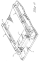
- an electrical connector 1 especially suitable for use in a card reader, not shown, includes an insulating housing 2 having a card receiving mouth 3 , Figure 2, multiple electrical contacts 4 held by the housing 2 extending in two rows and into the mouth 3, and a set of card guide arms 5 , 6 .
- Tail sections 7 of the contacts 4 extend outwardly of a rear surface 8 of the housing 2 for connection to a first circuit board 9 shown in phantom outline.
- Feet 10 on free ends of the contacts 4 are adapted with respective shapes for connection to the circuit board 9.
- the feet 10 are shaped as posts for insertion into plated apertures 11 of the circuit board 9.
- the feet 10 can be shaped as surface mount flat portions, not shown, for connection to surface mount pads on the circuit board 9, Figures 1, 2, 8, 14 and 16.
- the connector 1 is accompanied by a duplicate housing 2, inverted, accompanied by another set of inverted guide arms 5,6, not shown.
- a bottom surface 12 is on each housing 2 with a projecting knob or foot 13 , received in an alignment aperture 40 in the circuit board 9.
- Each housing 2 has starter grooves 14 in forwardly projecting housing arms 15 on opposite sides of the mouth 3.
- a top surface 16 of each housing 2 has a locking structure 17 in the form of a recess 18 on one side flanking the mouth 3, and a projecting knob 19 in another side flanking the mouth 3.
- the duplicate housings 2 can be stacked and interlocked, Figures 14 and 16, when inverted with respect to each other, with the recess 18 of each housing receiving the knob 19 of the other housing.
- Each housing 2 is constructed for use alone on the circuit board 9, Figures 1 and 2, or for interlocking with a duplicate housing 2, Figures 14 and 16.
- the card receiving mouth 3 is defined either by a single housing 2 or by two housings 2.
- the card receiving mouth 3 is adapted to receive one or, alternatively, two cards, one for each of the stacked housings 2.
- the cards are known in the industry, and are disclosed, for example, in U.S.A. 5,033.972.
- the stacked housings 2 can be mounted to a second, inverted circuit board 9, as an alternative to the first circuit board 9, as shown in Figure 1.
- the guide arms 5, 6 are of unitary construction molded from a thermoplastic material.
- Figure 1 card receiving grooves 22 on inside surfaces 23 extend along lengths of the respective guide arms 5, 6.
- Flared, groove mouths 24 at respective ends of the guide arms 5, 6 open into respective grooves 22 of the guide arms 5, 6.
- respective elongated prongs 25 extend outwardly.
- the prongs 25 lockingly engage in sockets 26 , the sockets 26 being in respective, exterior side surfaces 27 of the housing 2 flanking the mouth 3.
- the prongs 25 have respective cross sections that interfit slidably along grooves 28 in the respective, exterior side surfaces 27 of the housing 2.
- Ends of the prongs 25 have respective locking latches 31 with transverse, projecting fingers 32 .
- the fingers 32 are forced to bend resiliently as they traverse in respective grooves 28, until the fingers 32 emerge from ends 33 of the grooves 28 and unbend to register against transverse latch shoulders 34 at the ends 33 of the grooves 28. Thereby, the prongs 25 lockingly engage the sockets 26.
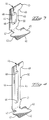
- the mounting bracket 41 of unitary construction is stamped and formed from a strip of metal, and comprises, a flat base 42 and at least one arm 45 projecting from the base.
- a hold down finger 49 extends laterally of the arm 45 in the thickness plane.
- a pair of wedge shaped projections 50 are spaced apart along the same arm 45 and extend laterally in the same direction as the hold down finger 49.
- a pair of coplanar arms 44 , 45 project from the base 42.
- the arms 44, 45 are joined by a first bight 46 joined to the base 42 by a thin, strain relieving, web 47 that is bendable when forces are applied to the arms 44, 45 to prevent transfer of the forces to the base 42, and thereby, prevent the forces from dislodging the base 42 from its solder connection.
- a second bight 48 bridges remote ends of the arms 44, 45.
- the base 42 of Figures 3, 4 and 15, is bent to extend transverse to the thickness plane of the arms 44, 45.
- the base 42 of Figures 3, 4, 6 and 15, has serpentine shaped edges 43 of serpentine lengths adapted to be wetted by molten solder, not shown, for solder connection of the base 42 to a conductive pad of the circuit board 9, Figures 1, 2 and 8, or the inverted circuit board 9, Figure 16.
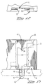
- the mounting bracket 41 is inserted along one of multiple channels 51 recessed in each of the side surfaces 27 of the housing 2.
- Each of the channels 51 is widened at opposite, open ends 52 to provide recessed ledges 53 in opposite sides 54 of the channel 51, with one of the ledges 53 being inverted.
- the hold down finger 49 overlaps the ledge 53 to hold the housing 2 against the first circuit board 9.
- the mounting bracket 41 is inverted, such that the hold down finger 49 overlaps the inverted ledge 53 while the base 42 is solder connected to a pad, not shown, on the inverted circuit board 9, and the inverted foot 9 of the stacked housing 2 received in an aperture 40 of the inverted circuit board 9.
- the projections 50 of the mounting bracket 41 wedge against a side 54 of the channel, and resiliently deflect the arm 45, such that the arms 44, 45 frictionally engage the opposite sides 54 of the channel 51.
- a channel 51 of similar construction is recessed in an exterior side 55 of each guide arm 5, 6, Figures 1, 2 and 9.
- Each of the channels 51 in the guide arms 5,6, and in the housings 2 is constructed with the two open ends 52 and the two ledges 53 to receive a mounting bracket 41 in an inverted position for solder connection of the mounting bracket 41 to the inverted circuit board 9, or, alternatively, to receive a mounting bracket 41 in a non-inverted position for solder connection to the first circuit board 9.
- flanges 56 overhang opposite sides 54 of each channel 51, to overlap edges of the arms 44, 45 of a mounting bracket 41 in the channel 51.
- One set of the flanges 56 on each side 55 of the housing 2 is divided into spaced apart segments 57 , Figure 16.
- Each of the flanges 56 overlies a portion of the hold down finger 49 and the projections 50 to maintain them in the plane of thickness of the mounting bracket 41.
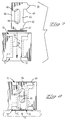
- the base 42 of Figures 5, 9, 10 and 13 comprises, a barbed, slotted post 58 defined by two barbed spring members 59 extending along opposite sides of a slot 60 having closed ends that join the spring members 59 together. Further details of the post 58 are disclosed in U.S. A. 4,907,987.
- the post 58 is adapted for insertion in an aperture 69 of the circuit board 9, Figure 13 instead of a pad as in the circuit board of Figures 1, 2, 8, 14 and 16.
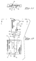
- a second finger 61 on the base 42 at an end of the arm 45 remote from the finger 49 is bent out of the plane of the arm 45, Figures 5, 6, 10 and 11, to pass between the spaced apart flanges 56, as the base 42 and the arm 45 are inserted along the channel 51.
- the second finger 61 is thereafter bent to return toward the plane of the arm 45, Figures 12 and 13, and to project laterally in the same direction as the finger 49, and to overlap a corresponding, recessed end of the channel 51.
- the shoulder 53 and the recessed end of the channel 51 are interposed between the fingers 49, 61, Figure 13, thereby to retain the mounting bracket 41.
Landscapes
- Engineering & Computer Science (AREA)
- Artificial Intelligence (AREA)
- Computer Vision & Pattern Recognition (AREA)
- Physics & Mathematics (AREA)
- General Physics & Mathematics (AREA)
- Theoretical Computer Science (AREA)
- Microelectronics & Electronic Packaging (AREA)
- Coupling Device And Connection With Printed Circuit (AREA)
- Multi-Conductor Connections (AREA)
- Details Of Connecting Devices For Male And Female Coupling (AREA)
Applications Claiming Priority (4)
| Application Number | Priority Date | Filing Date | Title |
|---|---|---|---|
| US987225 | 1992-12-08 | ||
| US986660 | 1992-12-08 | ||
| US07/986,660 US5308251A (en) | 1992-08-10 | 1992-12-08 | Mounting bracket with ESD protection for an electrical connector |
| US07/987,225 US5297966A (en) | 1992-08-10 | 1992-12-08 | Mounting bracket for an electrical connector |
Publications (2)
| Publication Number | Publication Date |
|---|---|
| EP0601703A1 true EP0601703A1 (fr) | 1994-06-15 |
| EP0601703B1 EP0601703B1 (fr) | 1997-01-15 |
Family
ID=27130635
Family Applications (1)
| Application Number | Title | Priority Date | Filing Date |
|---|---|---|---|
| EP93308526A Expired - Lifetime EP0601703B1 (fr) | 1992-12-08 | 1993-10-26 | Support pour le montage d'un connecteur électrique |
Country Status (5)
| Country | Link |
|---|---|
| EP (1) | EP0601703B1 (fr) |
| JP (1) | JP3016058B2 (fr) |
| KR (1) | KR940017006A (fr) |
| CN (1) | CN1088025A (fr) |
| DE (1) | DE69307482T2 (fr) |
Cited By (3)
| Publication number | Priority date | Publication date | Assignee | Title |
|---|---|---|---|---|
| EP0919944A3 (fr) * | 1997-11-25 | 2002-06-26 | Thomas & Betts Corporation | Appareil de lecture de cartes à puce |
| GB2406229A (en) * | 2003-09-17 | 2005-03-23 | Molex Inc | Memory card connector with side mounting locking means |
| WO2004105193A3 (fr) * | 2003-05-21 | 2005-04-07 | Molex Inc | Connecteur de carte memoire a construction de logement amelioree |
Families Citing this family (1)
| Publication number | Priority date | Publication date | Assignee | Title |
|---|---|---|---|---|
| JP2004087177A (ja) * | 2002-08-23 | 2004-03-18 | Tyco Electronics Amp Kk | カード接続構造及びそれに用いるカードコネクタ |
Citations (5)
| Publication number | Priority date | Publication date | Assignee | Title |
|---|---|---|---|---|
| DE8704410U1 (de) * | 1987-03-25 | 1987-05-21 | Philips Patentverwaltung Gmbh, 2000 Hamburg | Halter für elektrische Bauelemente |
| US4952161A (en) * | 1988-03-03 | 1990-08-28 | Hosiden Electronics Co., Ltd. | Card connector |
| US5033972A (en) * | 1990-04-26 | 1991-07-23 | Hosiden Corporation | Electrical connector |
| US5171165A (en) * | 1991-06-28 | 1992-12-15 | Foxconn International | Electrical connector incorporating an improved hold-down device for securing to a printed circuit board, or the like |
| DE9217302U1 (de) * | 1992-12-17 | 1993-02-25 | Siemens AG, 8000 München | Kunststoffträger zur Aufnahme und Halterung eines elektronischen Moduls |
-
1993
- 1993-10-26 EP EP93308526A patent/EP0601703B1/fr not_active Expired - Lifetime
- 1993-10-26 DE DE69307482T patent/DE69307482T2/de not_active Expired - Lifetime
- 1993-12-07 KR KR1019930026650A patent/KR940017006A/ko not_active Ceased
- 1993-12-07 CN CN93120856A patent/CN1088025A/zh active Pending
- 1993-12-08 JP JP5340662A patent/JP3016058B2/ja not_active Expired - Lifetime
Patent Citations (5)
| Publication number | Priority date | Publication date | Assignee | Title |
|---|---|---|---|---|
| DE8704410U1 (de) * | 1987-03-25 | 1987-05-21 | Philips Patentverwaltung Gmbh, 2000 Hamburg | Halter für elektrische Bauelemente |
| US4952161A (en) * | 1988-03-03 | 1990-08-28 | Hosiden Electronics Co., Ltd. | Card connector |
| US5033972A (en) * | 1990-04-26 | 1991-07-23 | Hosiden Corporation | Electrical connector |
| US5171165A (en) * | 1991-06-28 | 1992-12-15 | Foxconn International | Electrical connector incorporating an improved hold-down device for securing to a printed circuit board, or the like |
| DE9217302U1 (de) * | 1992-12-17 | 1993-02-25 | Siemens AG, 8000 München | Kunststoffträger zur Aufnahme und Halterung eines elektronischen Moduls |
Cited By (3)
| Publication number | Priority date | Publication date | Assignee | Title |
|---|---|---|---|---|
| EP0919944A3 (fr) * | 1997-11-25 | 2002-06-26 | Thomas & Betts Corporation | Appareil de lecture de cartes à puce |
| WO2004105193A3 (fr) * | 2003-05-21 | 2005-04-07 | Molex Inc | Connecteur de carte memoire a construction de logement amelioree |
| GB2406229A (en) * | 2003-09-17 | 2005-03-23 | Molex Inc | Memory card connector with side mounting locking means |
Also Published As
| Publication number | Publication date |
|---|---|
| CN1088025A (zh) | 1994-06-15 |
| JP3016058B2 (ja) | 2000-03-06 |
| EP0601703B1 (fr) | 1997-01-15 |
| JPH06215834A (ja) | 1994-08-05 |
| KR940017006A (ko) | 1994-07-25 |
| DE69307482D1 (de) | 1997-02-27 |
| DE69307482T2 (de) | 1997-08-07 |
Similar Documents
| Publication | Publication Date | Title |
|---|---|---|
| US5297966A (en) | Mounting bracket for an electrical connector | |
| US5290174A (en) | Electrical connector for a card reader | |
| US5004434A (en) | Printed circuit board edge connector | |
| US5308251A (en) | Mounting bracket with ESD protection for an electrical connector | |
| US5112233A (en) | Electrical connector having contact retention means | |
| US5192228A (en) | Shielded surface mount electrical connector with integral barbed board lock | |
| US3720907A (en) | Panel connector employing flag-type terminals and terminal extracting tool for the same | |
| US5582519A (en) | Make-first-break-last ground connections | |
| US5194017A (en) | Connector for a flexible circuit | |
| EP0590429B1 (fr) | Connecteur éléctrique de bordure de carte | |
| US4880401A (en) | Electric female connector piece | |
| EP0658958A2 (fr) | Boîtier pour connecteur en bordure de carte à pièces multiples et bras de montage | |
| JP3360178B2 (ja) | 一体的支持構造を有する電気コネクタ | |
| EP0472006A1 (fr) | Connecteur électrique avec moyens pour garantir une connexion électrique fiable | |
| US6039590A (en) | Electrical connector with relatively movable two-part housing | |
| EP0717468B1 (fr) | Connecteur interrompant d'abord les contacts polaires et après le contact à la terre | |
| JPH1021981A (ja) | 基板用電気コネクタ | |
| JPS598035B2 (ja) | ゼロ插抜力コネクタ− | |
| CA1265221A (fr) | Borne de connexion electrique pour connecteur | |
| US6471534B1 (en) | Electrical contact for ZIF socket connector | |
| EP0851539A2 (fr) | Connecteur pour des câbles plats | |
| US5575663A (en) | Electrical connector for mounting to an edge of a circuit board | |
| EP0542068A2 (fr) | Contact électrique femelle | |
| US6554633B1 (en) | Electrical contact for ZIF socket connector | |
| KR101053753B1 (ko) | 커넥터 |
Legal Events
| Date | Code | Title | Description |
|---|---|---|---|
| PUAI | Public reference made under article 153(3) epc to a published international application that has entered the european phase |
Free format text: ORIGINAL CODE: 0009012 |
|
| AK | Designated contracting states |
Kind code of ref document: A1 Designated state(s): DE FR GB |
|
| 17P | Request for examination filed |
Effective date: 19941128 |
|
| 17Q | First examination report despatched |
Effective date: 19951120 |
|
| GRAH | Despatch of communication of intention to grant a patent |
Free format text: ORIGINAL CODE: EPIDOS IGRA |
|
| GRAH | Despatch of communication of intention to grant a patent |
Free format text: ORIGINAL CODE: EPIDOS IGRA |
|
| GRAA | (expected) grant |
Free format text: ORIGINAL CODE: 0009210 |
|
| AK | Designated contracting states |
Kind code of ref document: B1 Designated state(s): DE FR GB |
|
| REF | Corresponds to: |
Ref document number: 69307482 Country of ref document: DE Date of ref document: 19970227 |
|
| ET | Fr: translation filed | ||
| ET | Fr: translation filed |
Free format text: CORRECTIONS |
|
| PLBE | No opposition filed within time limit |
Free format text: ORIGINAL CODE: 0009261 |
|
| 26N | No opposition filed | ||
| REG | Reference to a national code |
Ref country code: GB Ref legal event code: IF02 |
|
| PGFP | Annual fee paid to national office [announced via postgrant information from national office to epo] |
Ref country code: FR Payment date: 20121107 Year of fee payment: 20 Ref country code: DE Payment date: 20121029 Year of fee payment: 20 |
|
| PGFP | Annual fee paid to national office [announced via postgrant information from national office to epo] |
Ref country code: GB Payment date: 20121025 Year of fee payment: 20 |
|
| REG | Reference to a national code |
Ref country code: DE Ref legal event code: R071 Ref document number: 69307482 Country of ref document: DE |
|
| REG | Reference to a national code |
Ref country code: GB Ref legal event code: PE20 Expiry date: 20131025 |
|
| PG25 | Lapsed in a contracting state [announced via postgrant information from national office to epo] |
Ref country code: GB Free format text: LAPSE BECAUSE OF EXPIRATION OF PROTECTION Effective date: 20131025 Ref country code: DE Free format text: LAPSE BECAUSE OF EXPIRATION OF PROTECTION Effective date: 20131029 |