EP0601951A2 - Procédé pour améliorer la résistance de couche d'un dispositif comportant un transistor à effet de champ - Google Patents
Procédé pour améliorer la résistance de couche d'un dispositif comportant un transistor à effet de champ Download PDFInfo
- Publication number
- EP0601951A2 EP0601951A2 EP93480201A EP93480201A EP0601951A2 EP 0601951 A2 EP0601951 A2 EP 0601951A2 EP 93480201 A EP93480201 A EP 93480201A EP 93480201 A EP93480201 A EP 93480201A EP 0601951 A2 EP0601951 A2 EP 0601951A2
- Authority
- EP
- European Patent Office
- Prior art keywords
- gate
- layer
- insulating layer
- sheet resistance
- passivating layer
- Prior art date
- Legal status (The legal status is an assumption and is not a legal conclusion. Google has not performed a legal analysis and makes no representation as to the accuracy of the status listed.)
- Ceased
Links
Images
Classifications
-
- H—ELECTRICITY
- H10—SEMICONDUCTOR DEVICES; ELECTRIC SOLID-STATE DEVICES NOT OTHERWISE PROVIDED FOR
- H10P—GENERIC PROCESSES OR APPARATUS FOR THE MANUFACTURE OR TREATMENT OF DEVICES COVERED BY CLASS H10
- H10P95/00—Generic processes or apparatus for manufacture or treatments not covered by the other groups of this subclass
-
- H—ELECTRICITY
- H10—SEMICONDUCTOR DEVICES; ELECTRIC SOLID-STATE DEVICES NOT OTHERWISE PROVIDED FOR
- H10W—GENERIC PACKAGES, INTERCONNECTIONS, CONNECTORS OR OTHER CONSTRUCTIONAL DETAILS OF DEVICES COVERED BY CLASS H10
- H10W20/00—Interconnections in chips, wafers or substrates
- H10W20/01—Manufacture or treatment
- H10W20/071—Manufacture or treatment of dielectric parts thereof
- H10W20/081—Manufacture or treatment of dielectric parts thereof by forming openings in the dielectric parts
-
- Y—GENERAL TAGGING OF NEW TECHNOLOGICAL DEVELOPMENTS; GENERAL TAGGING OF CROSS-SECTIONAL TECHNOLOGIES SPANNING OVER SEVERAL SECTIONS OF THE IPC; TECHNICAL SUBJECTS COVERED BY FORMER USPC CROSS-REFERENCE ART COLLECTIONS [XRACs] AND DIGESTS
- Y10—TECHNICAL SUBJECTS COVERED BY FORMER USPC
- Y10S—TECHNICAL SUBJECTS COVERED BY FORMER USPC CROSS-REFERENCE ART COLLECTIONS [XRACs] AND DIGESTS
- Y10S438/00—Semiconductor device manufacturing: process
- Y10S438/934—Sheet resistance, i.e. dopant parameters
Definitions
- the present invention relates generally to fabrication of Field Efficient Transistor devices. More particularly, the present invention relates to a process for improving sheet resistance of a FET device gate during fabrication.
- Agglomeration refers to formation of non-uniformities in the TiSi e , such as peaks, pits, or areas where TiSi e has not formed.
- a proposed solution has been to deposit more Ti, but shallow junction depth requirements preclude this due to junction leakage concerns.
- the aforementioned process may not integrate efficiently into subsequent processing steps.
- a special non-reflective film titanium nitride is required to insure proper photolithography, and a special etching process is required to control polycrystalline silicon gate dimensions, since the presence of titanium may cause etching difficulties.
- a second approach involves metal silicide deposition using chemical vapor deposition (CVD) .
- This second approach suffers from an incorporation of impurities into the gate.
- WF6 tungsten hexafluoride
- the CVD process results in fluorine incorporation into the gate.
- the amount of fluorine incorporated directly affects gate oxide thickness, which determines how well the gate couples with the source and drain.
- tungsten if tungsten is used, its resistivity as a silicide is much larger than that of TiSi e . The result is a thicker gate stack to achieve a given sheet resistance, which may be unacceptable in subsequent processing steps.
- CVD is typically not stoichiometric (a two-to-one silicone-to-metal ratio)
- this second approach requires an anneal to drive off excess silicon, which may be at too high a temperature for some applications.
- the present invention provides a process for achieving improved sheet resistance of a FET device gate with shallow source and drain regions, utilizing the silicidation approach, by introducing a passivating layer used as both a polish stop and an etch stop.
- a passivating layer used as both a polish stop and an etch stop.
- the gate top is then exposed by removing the passivating layer above the gate selective to the insulating layer and gate stack.
- selective to refers to the passivating layer above the gate being removed with little or no removal of the insulating layer and gate stack.
- a trench is created above one or both junctions by etching the insulation layer, using the passivating layer as an etch stop. The trench is extended through the passivating layer selective to the junction.
- the area above the gate as well as the extended trench can then each be filled with a low sheet resistance conductive material, creating low resistance contacts to the gate and junction.
- the contact to the junction is borderless. That is, it partially contacts the junction and an isolation region in the substrate next to the junction.
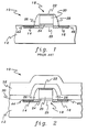
- FIG. 1 presents a cross-sectional view of a FET device fabricated according to conventional processes.
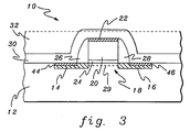
- FIG. 2 depicts the FET device of FIG. 1 with a passivating layer deposited on the FET device and an insulating layer deposited on the passivating layer, according to the present invention.
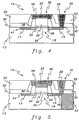
- FIG. 3 depicts the FET device of FIG. 2 after planarization of the insulating layer and planar polishing beyond planarization to the passivating layer.
- FIG. 4 depicts the FET device of FIG. 3 after the passivating layer is selectively removed above the gate, a trench is created above a junction, and the opening above the gate and the trench are each planarly filled with a low sheet resistance conductive material, creating low resistance contacts to the source and junction.
- FIG. 5 depicts a FET device fabricated according to a second embodiment of the process of the present invention.
- FIG. 1 depicts a FET device 10 conventionally fabricated.
- Silicon substrate 12 has junctions 14 and 16 implanted therein. Each junction may be a source or a drain. Junctions 14 and 16 are activated; that is, they have previously been doped with n-type or p-type dopants. The junctions are then silicided. That is, the regions of substrate 12 where junctions 14 and 16 are shown are reacted with a refractory metal, such as titanium or cobalt, forming an intermetallic compound with the silicon known as silicide. It will be understood that the junctions need not have been activated prior to silicidation, except that the present embodiment utilizes Ti as the silicide material. Activation requires high heat cycles, which TiSi e cannot tolerate. Thus, activation must precede silicidation when Ti is used.
- a gate stack 18 is formed on substrate 12 between junctions 14 and 16.
- Gate stack 18 is, for example, made of doped polycrystalline silicon (polysilicon).
- Gate stack 18 may be n+ doped, p + doped, or both n+ and p + doped (dual doped). Included in gate stack 18 may be an at least partially silicided portion 22 and an unsilicided portion 20.
- junctions 14 and 16 Prior to silicidation, creating junctions 14 and 16, the area of substrate 12 including the junctions and diffusion region 29 was one large diffusion region. After creation of gate stack 18 and the spacers were placed, silicidation created junctions 14 and 16, while the spacers and gate stack insulated diffusion region 29 from the silicide material.
- the spacers could comprise, for example, silicon nitride.
- the purpose of diffusion region 29 is to control the threshold voltages of the FET device 10.
- a passivating layer 30 is applied over the FET structure and then an insulating layer 32 is applied over passivating layer 30.
- passivating layer 30 is conformally applied.
- FIG. 2 shows the FET device 10 of FIG. 1 after passivating layer 30 and insulating layer 32 have been deposited.
- the insulating and passivating layers may be deposited, for example, by conventional chemical vapor deposition processes that are well-known in the art.
- the thin passivating layer nominally about 100 nm thick, may comprise silicon nitride and provides protection against ionics (e.g., sodium).
- the passivating layer serves as a polish stop, since it is chosen to polish significantly slower than the insulating layer, and also serves as an etch stop, since the etch chemistries for the two layers are different.
- the insulating layer separates the FET device 10 from subsequent metal layers and could be, for example, phosphosilicate glass (P5G) on the order of 350 nm thick, or gate stack height (here, 200 nm) plus 150 nm.
- Planarization of insulating layer 32 then takes place. Planarization can be accomplished, for example, by utilizing a planarization blocking mask (e.g., photoresist) with reactive ion etching. Reactive ion etching is well-known in the art and accordingly need not be further described herein.
- FIG. 3 depicts the FET device of FIG. 2 after planarization of insulating layer 32. Planarization of insulating layer 32 is then done to expose passivating layer 30 above gate stack 18, as shown by dashed line 34.
- CMP chemical-mechanical polishing
- CMP is well-known in the art. That the passivating layer works well as a polish stop is exemplified by using the example insulating and passivating layer compositions. The polish rate of PSG compared to silicon nitride is about four-to-one.
- the portion of passivating layer 32 above gate stack 18 is removed as shown in FIG. 4.
- reactive ion etching may be used to open trench 36.
- the etch rate of nitride compared to PSG is about 3-to-1
- the etch rate of nitride compared to polycrystalline silicon is about 5.5-to-1.
- passivating layer 30 is removed to form trench 36 selective to insulating layer 32 and gate stack 18. That is, passivating layer 30 is removed, while removing very little of insulating layer 32 or gate stack 18. It will be understood that although spacers 26 and 28 are shown partially removed in FIG. 4, they need not be.
- the example composition of spacers 26 and 28 is silicon nitride, which the etch chemistry for creating trench 36 in PSG passivating layer 30 is not selective to.
- Another composition may be chosen for the spacers, so that the etch chemistry would be selective to it.
- a trench above one or both of the junctions is created, utilizing the passivating layer 30 as an etch stop.
- a trench 40 is created above a junction in the insulating layer selective to the passivating layer.
- Trench 40 is then extended through passivating layer 30, selective to junction 16. That is, the etching process used to extend trench 40 to expose junction 16 is chosen such that little or none of junction 16 is affected.
- trench 40 could be formed using reactive ion etching and merely changing the chemistry used after exposing the passivating layer. Such techniques are well-known in the art and need not be further explained.
- Trenches 36 and 40 may now be filled with a low sheet resistance conductive material 38, such as tungsten, creating contacts to the gate stack 18 and junction 16.
- sheet resistance refers to resistance per area of thin materials.
- the material 38 should be kept planar with the now- planarized insulating layer 32 in contemplation of the next level processing. It will be understood that trenches 36 and 40 could each be filled with a different material having the low street resistance property. It will also be understood that trenches 36 and 40 could be filled with insulation and then a hole bore through that is then filled with a low sheet resistance conductive material.
- a gate stack initially comprising 200 nm of undoped polysilicon.
- 36 nm of titanium are deposited on the gate stack.
- the titanium reacts with the polysilicon to form a maximum of 54,5 nM of TiSi e
- 74 nm of Ti are deposited over the gate stack.
- a maximun of 111,5 nm of additional TiSi e are formed on the gate stack, giving a total maximum TiSi e gate stack portion of 166 nm.
- a minimum of 50 nm of polysilicon is left on the gate stack between the TiSi2 and the dielectric layer after enhanced silicidation. It will be understood that if the polysilicon were doped, all maximum values given would be lower.
- FIG. 5 depicts the FET device 10 of FIG. 4 with an isolation region 42 provided in substrate 12 adjacent to junction 16, and trench 41 filled to create a borderless contact. Isolation regions separate devices on a wafer and many comprise, for example, silicon dioxide.
- a trench 41 is first created in insulating layer 32 above both junction 16 and isolation region 42 selective to passivating layer 30. The trench is then extended through passivating layer 30 selective to and partially exposing junction 16 and isolation region 42.
- Trenches 36 and 41 may now be planarly filled with a low sheet resistance conductive material 38 simultaneously. This could be accomplished by depositing a layer of material 38 over insulating layer 32 and trenches 36 and 41, then removing the unwanted portion. This creates low resistance contacts to junction 16 and gate stack 18. As in the first embodiment, the material filling trench 36 need not be the same as for trench 41.
- the characterization of the contact to junction 16 as "borderless" refers to the partial incursion into the area above isolation region 42. If the contact was only above junction 16, it would not be borderless. Making the contact borderless has a distinct advantage, in that density is gained. Present design criteria set a minimum distance between gate stack 18 and the junction contact. A given size for the contact thus would require a larger junction 16 in order to be completely within the region above junction 16 and still be at the minimum distance from gate stack 18.
- the present invention advances the state of the art by providing a process for improving sheet resistance of a FET device gate in a silicidation fabrication scheme.
- a dual-use passivation layer is introduced, acting as both a polish stop for planarization and an etch stop for creation of contacts.
- the process integrates easily into existing fabrication processes. Further, enhanced silicidation of the gate is also facilitated without affecting shallow source and drain regions, and avoiding agglomeration.
- a contact to one or both junctions may be borderless to increase density.
Landscapes
- Electrodes Of Semiconductors (AREA)
- Insulated Gate Type Field-Effect Transistor (AREA)
Applications Claiming Priority (2)
| Application Number | Priority Date | Filing Date | Title |
|---|---|---|---|
| US989604 | 1992-12-11 | ||
| US07/989,604 US5268330A (en) | 1992-12-11 | 1992-12-11 | Process for improving sheet resistance of an integrated circuit device gate |
Publications (2)
| Publication Number | Publication Date |
|---|---|
| EP0601951A2 true EP0601951A2 (fr) | 1994-06-15 |
| EP0601951A3 EP0601951A3 (fr) | 1995-01-04 |
Family
ID=25535264
Family Applications (1)
| Application Number | Title | Priority Date | Filing Date |
|---|---|---|---|
| EP93480201A Ceased EP0601951A3 (fr) | 1992-12-11 | 1993-11-19 | Procédé pour améliorer la résistance de couche d'un dispositif comportant un transistor à effet de champ. |
Country Status (3)
| Country | Link |
|---|---|
| US (1) | US5268330A (fr) |
| EP (1) | EP0601951A3 (fr) |
| JP (1) | JPH07105500B2 (fr) |
Cited By (2)
| Publication number | Priority date | Publication date | Assignee | Title |
|---|---|---|---|---|
| WO2000075967A3 (fr) * | 1999-06-03 | 2001-07-05 | Advanced Micro Devices Inc | Procede de fabrication d'une grille de transistor mosfet a faible resistivite recouverte d'une faible couche de siliciure metallique sur du silicium polycristallin |
| WO2004019383A3 (fr) * | 2002-08-22 | 2004-04-08 | Intel Corp | Contacts autoalignes vis-a-vis des grilles |
Families Citing this family (77)
| Publication number | Priority date | Publication date | Assignee | Title |
|---|---|---|---|---|
| US5604159A (en) * | 1994-01-31 | 1997-02-18 | Motorola, Inc. | Method of making a contact structure |
| US5650654A (en) * | 1994-12-30 | 1997-07-22 | International Business Machines Corporation | MOSFET device having controlled parasitic isolation threshold voltage |
| JP3022744B2 (ja) * | 1995-02-21 | 2000-03-21 | 日本電気株式会社 | 半導体装置及びその製造方法 |
| US5652176A (en) * | 1995-02-24 | 1997-07-29 | Motorola, Inc. | Method for providing trench isolation and borderless contact |
| US6376911B1 (en) | 1995-08-23 | 2002-04-23 | International Business Machines Corporation | Planarized final passivation for semiconductor devices |
| US5702981A (en) * | 1995-09-29 | 1997-12-30 | Maniar; Papu D. | Method for forming a via in a semiconductor device |
| US5683941A (en) * | 1996-07-02 | 1997-11-04 | National Semiconductor Corporation | Self-aligned polycide process that utilizes a planarized layer of material to expose polysilicon structures to a subsequently deposited metal layer that is reacted to form the metal silicide |
| US7041548B1 (en) * | 1996-07-16 | 2006-05-09 | Micron Technology, Inc. | Methods of forming a gate stack that is void of silicon clusters within a metallic silicide film thereof |
| US6087254A (en) * | 1996-07-16 | 2000-07-11 | Micron Technology, Inc. | Technique for elimination of pitting on silicon substrate during gate stack etch |
| US6613673B2 (en) | 1996-07-16 | 2003-09-02 | Micron Technology, Inc. | Technique for elimination of pitting on silicon substrate during gate stack etch |
| US7078342B1 (en) | 1996-07-16 | 2006-07-18 | Micron Technology, Inc. | Method of forming a gate stack |
| JP3217015B2 (ja) * | 1996-07-18 | 2001-10-09 | インターナショナル・ビジネス・マシーンズ・コーポレーション | 電界効果トランジスタの形成方法 |
| US6870232B1 (en) | 1996-07-18 | 2005-03-22 | International Business Machines Corporation | Scalable MOS field effect transistor |
| FR2757312B1 (fr) * | 1996-12-16 | 1999-01-08 | Commissariat Energie Atomique | Transistor mis a grille metallique auto-alignee et son procede de fabrication |
| US5953635A (en) * | 1996-12-19 | 1999-09-14 | Intel Corporation | Interlayer dielectric with a composite dielectric stack |
| US5908659A (en) * | 1997-01-03 | 1999-06-01 | Mosel Vitelic Inc. | Method for reducing the reflectivity of a silicide layer |
| TW320744B (en) * | 1997-01-15 | 1997-11-21 | Winbond Electronics Corp | Manufacturing method of self-aligned salicide |
| TW329553B (en) * | 1997-02-04 | 1998-04-11 | Winbond Electronics Corp | The semiconductor manufacturing process for two-step salicide |
| US5985768A (en) * | 1997-04-30 | 1999-11-16 | International Business Machines Corporation | Method of forming a semiconductor |
| US5953612A (en) * | 1997-06-30 | 1999-09-14 | Vlsi Technology, Inc. | Self-aligned silicidation technique to independently form silicides of different thickness on a semiconductor device |
| US6143613A (en) * | 1997-06-30 | 2000-11-07 | Vlsi Technology, Inc. | Selective exclusion of silicide formation to make polysilicon resistors |
| US6207543B1 (en) | 1997-06-30 | 2001-03-27 | Vlsi Technology, Inc. | Metallization technique for gate electrodes and local interconnects |
| US6074921A (en) * | 1997-06-30 | 2000-06-13 | Vlsi Technology, Inc. | Self-aligned processing of semiconductor device features |
| US6420273B1 (en) | 1997-06-30 | 2002-07-16 | Koninklijke Philips Electronics N.V. | Self-aligned etch-stop layer formation for semiconductor devices |
| US5827768A (en) * | 1997-07-07 | 1998-10-27 | National Science Council | Method for manufacturing an MOS transistor having a self-aligned and planarized raised source/drain structure |
| US7009264B1 (en) * | 1997-07-30 | 2006-03-07 | Micron Technology, Inc. | Selective spacer to prevent metal oxide formation during polycide reoxidation |
| US5925918A (en) * | 1997-07-30 | 1999-07-20 | Micron, Technology, Inc. | Gate stack with improved sidewall integrity |
| US5955759A (en) * | 1997-12-11 | 1999-09-21 | International Business Machines Corporation | Reduced parasitic resistance and capacitance field effect transistor |
| US5966597A (en) * | 1998-01-06 | 1999-10-12 | Altera Corporation | Method of forming low resistance gate electrodes |
| US6001697A (en) * | 1998-03-24 | 1999-12-14 | Mosel Vitelic Inc. | Process for manufacturing semiconductor devices having raised doped regions |
| US6015751A (en) * | 1998-04-06 | 2000-01-18 | Taiwan Semiconductor Manufacturing Company | Self-aligned connection to underlayer metal lines through unlanded via holes |
| KR100268459B1 (ko) * | 1998-05-07 | 2000-10-16 | 윤종용 | 반도체 장치의 콘택 플러그 형성 방법 |
| US6235598B1 (en) * | 1998-11-13 | 2001-05-22 | Intel Corporation | Method of using thick first spacers to improve salicide resistance on polysilicon gates |
| US6501098B2 (en) * | 1998-11-25 | 2002-12-31 | Semiconductor Energy Laboratory Co, Ltd. | Semiconductor device |
| US6015747A (en) * | 1998-12-07 | 2000-01-18 | Advanced Micro Device | Method of metal/polysilicon gate formation in a field effect transistor |
| TW432614B (en) * | 1998-12-23 | 2001-05-01 | United Microelectronics Corp | Manufacturing method for self-aligned contact |
| US6534393B1 (en) | 1999-01-25 | 2003-03-18 | Chartered Semiconductor Manufacturing Ltd. | Method for fabricating local metal interconnections with low contact resistance and gate electrodes with improved electrical conductivity |
| US6235593B1 (en) * | 1999-02-18 | 2001-05-22 | Taiwan Semiconductor Manufacturing Company | Self aligned contact using spacers on the ILD layer sidewalls |
| US6174762B1 (en) | 1999-03-02 | 2001-01-16 | International Business Machines Corporation | Salicide device with borderless contact |
| US6461951B1 (en) * | 1999-03-29 | 2002-10-08 | Advanced Micro Devices, Inc. | Method of forming a sidewall spacer to prevent gouging of device junctions during interlayer dielectric etching including silicide growth over gate spacers |
| US6294823B1 (en) | 1999-05-12 | 2001-09-25 | Intel Corporation | Integrated circuit with insulating spacers separating borderless contacts from the well |
| US6228777B1 (en) * | 1999-06-08 | 2001-05-08 | Intel Corporation | Integrated circuit with borderless contacts |
| US6329118B1 (en) | 1999-06-21 | 2001-12-11 | Intel Corporation | Method for patterning dual damascene interconnects using a sacrificial light absorbing material |
| US6265302B1 (en) | 1999-07-12 | 2001-07-24 | Chartered Semiconductor Manufacturing Ltd. | Partially recessed shallow trench isolation method for fabricating borderless contacts |
| US6297126B1 (en) | 1999-07-12 | 2001-10-02 | Chartered Semiconductor Manufacturing Ltd. | Silicon nitride capped shallow trench isolation method for fabricating sub-micron devices with borderless contacts |
| US6171910B1 (en) * | 1999-07-21 | 2001-01-09 | Motorola Inc. | Method for forming a semiconductor device |
| US6046103A (en) * | 1999-08-02 | 2000-04-04 | Taiwan Semiconductor Manufacturing Company | Borderless contact process for a salicide devices |
| US6225225B1 (en) | 1999-09-09 | 2001-05-01 | Chartered Semiconductor Manufacturing Ltd. | Method to form shallow trench isolation structures for borderless contacts in an integrated circuit |
| JP2001237422A (ja) * | 1999-12-14 | 2001-08-31 | Sanyo Electric Co Ltd | 半導体装置およびその製造方法 |
| US6630721B1 (en) * | 2000-05-16 | 2003-10-07 | Advanced Micro Devices, Inc. | Polysilicon sidewall with silicide formation to produce high performance MOSFETS |
| KR100399363B1 (ko) * | 2001-01-11 | 2003-09-26 | 삼성전자주식회사 | 반도체 장치 및 그 형성 방법 |
| US6465294B1 (en) | 2001-03-16 | 2002-10-15 | Taiwan Semiconductor Manufacturing Company | Self-aligned process for a stacked gate RF MOSFET device |
| US6784098B1 (en) * | 2001-04-30 | 2004-08-31 | Taiwan Semiconductor Manufacturing Company | Method for forming salicide process |
| US6376351B1 (en) | 2001-06-28 | 2002-04-23 | Taiwan Semiconductor Manufacturing Company | High Fmax RF MOSFET with embedded stack gate |
| US6613623B1 (en) * | 2001-08-20 | 2003-09-02 | Taiwan Semiconductor Manufacturing Company | High fMAX deep submicron MOSFET |
| JP3574644B2 (ja) * | 2002-11-20 | 2004-10-06 | 沖電気工業株式会社 | 半導体装置の製造方法 |
| US7115479B2 (en) * | 2002-11-26 | 2006-10-03 | Intel Corporation | Sacrificial annealing layer for a semiconductor device and a method of fabrication |
| US7196013B2 (en) * | 2002-12-12 | 2007-03-27 | Intel Corporation | Capping layer for a semiconductor device and a method of fabrication |
| US6924184B2 (en) * | 2003-03-21 | 2005-08-02 | Freescale Semiconductor, Inc. | Semiconductor device and method for forming a semiconductor device using post gate stack planarization |
| TWI463526B (zh) * | 2004-06-24 | 2014-12-01 | 萬國商業機器公司 | 改良具應力矽之cmos元件的方法及以該方法製備而成的元件 |
| US7026689B2 (en) * | 2004-08-27 | 2006-04-11 | Taiwan Semiconductor Manufacturing Company | Metal gate structure for MOS devices |
| US7655511B2 (en) | 2005-11-03 | 2010-02-02 | International Business Machines Corporation | Gate electrode stress control for finFET performance enhancement |
| US7635620B2 (en) * | 2006-01-10 | 2009-12-22 | International Business Machines Corporation | Semiconductor device structure having enhanced performance FET device |
| US7488685B2 (en) | 2006-04-25 | 2009-02-10 | Micron Technology, Inc. | Process for improving critical dimension uniformity of integrated circuit arrays |
| US20070296052A1 (en) | 2006-06-26 | 2007-12-27 | Taiwan Semiconductor Manufacturing Company, Ltd. | Methods of forming silicide regions and resulting MOS devices |
| US7790540B2 (en) | 2006-08-25 | 2010-09-07 | International Business Machines Corporation | Structure and method to use low k stress liner to reduce parasitic capacitance |
| US7601574B2 (en) * | 2006-10-25 | 2009-10-13 | Globalfoundries Inc. | Methods for fabricating a stress enhanced MOS transistor |
| KR100869744B1 (ko) * | 2006-12-29 | 2008-11-21 | 동부일렉트로닉스 주식회사 | 씨모스 이미지 센서 및 그 제조방법 |
| US7550808B2 (en) * | 2007-01-18 | 2009-06-23 | International Business Machines Corporation | Fully siliciding regions to improve performance |
| US20080233703A1 (en) * | 2007-03-21 | 2008-09-25 | Atmel Corporation | Polysilicon conductivity improvement in a salicide process technology |
| US8115254B2 (en) | 2007-09-25 | 2012-02-14 | International Business Machines Corporation | Semiconductor-on-insulator structures including a trench containing an insulator stressor plug and method of fabricating same |
| US8492846B2 (en) | 2007-11-15 | 2013-07-23 | International Business Machines Corporation | Stress-generating shallow trench isolation structure having dual composition |
| KR20110101967A (ko) * | 2010-03-10 | 2011-09-16 | 삼성전자주식회사 | 반도체 소자 및 이를 제조하는 방법 |
| US8598006B2 (en) | 2010-03-16 | 2013-12-03 | International Business Machines Corporation | Strain preserving ion implantation methods |
| US10840105B2 (en) * | 2015-06-15 | 2020-11-17 | Taiwan Semiconductor Manufacturing Co., Ltd. | Gate structure with insulating structure and method for manufacturing the same |
| US10418453B2 (en) * | 2017-11-22 | 2019-09-17 | Taiwan Semiconductor Manufacturing Co., Ltd. | Forming metal contacts on metal gates |
| US11276682B1 (en) * | 2020-09-01 | 2022-03-15 | Newport Fab, Llc | Nickel silicide in bipolar complementary-metal-oxide-semiconductor (BiCMOS) device and method of manufacturing |
Family Cites Families (20)
| Publication number | Priority date | Publication date | Assignee | Title |
|---|---|---|---|---|
| FR2537779B1 (fr) * | 1982-12-10 | 1986-03-14 | Commissariat Energie Atomique | Procede de positionnement d'un trou de contact electrique entre deux lignes d'interconnexion d'un circuit integre |
| US4587718A (en) * | 1984-11-30 | 1986-05-13 | Texas Instruments Incorporated | Process for forming TiSi2 layers of differing thicknesses in a single integrated circuit |
| SE453547B (sv) * | 1985-03-07 | 1988-02-08 | Stiftelsen Inst Mikrovags | Forfarande vid framstellning av integrerade kretsar der pa en substratplatta ledare och s k gate-strukturer uppbygges |
| US4746219A (en) * | 1986-03-07 | 1988-05-24 | Texas Instruments Incorporated | Local interconnect |
| US4690730A (en) * | 1986-03-07 | 1987-09-01 | Texas Instruments Incorporated | Oxide-capped titanium silicide formation |
| US4877775A (en) * | 1986-06-16 | 1989-10-31 | E. I. Du Pont De Nemours And Company | Polymeric aminosaccharides as antihypercholesterolemic agents |
| FR2603128B1 (fr) * | 1986-08-21 | 1988-11-10 | Commissariat Energie Atomique | Cellule de memoire eprom et son procede de fabrication |
| ATE87766T1 (de) * | 1986-11-18 | 1993-04-15 | Siemens Ag | Integrierte halbleiterschaltung mit als duennschichtstege auf den die aktiven transistorbereiche trennenden feldoxidbereichen angeordneten lastwiderstaende und verfahren zu ihrer herstellung. |
| US4795722A (en) * | 1987-02-05 | 1989-01-03 | Texas Instruments Incorporated | Method for planarization of a semiconductor device prior to metallization |
| US4753709A (en) * | 1987-02-05 | 1988-06-28 | Texas Instuments Incorporated | Method for etching contact vias in a semiconductor device |
| US4824521A (en) * | 1987-04-01 | 1989-04-25 | Fairchild Semiconductor Corporation | Planarization of metal pillars on uneven substrates |
| US4994402A (en) * | 1987-06-26 | 1991-02-19 | Hewlett-Packard Company | Method of fabricating a coplanar, self-aligned contact structure in a semiconductor device |
| US4755478A (en) * | 1987-08-13 | 1988-07-05 | International Business Machines Corporation | Method of forming metal-strapped polysilicon gate electrode for FET device |
| US4966870A (en) * | 1988-04-14 | 1990-10-30 | International Business Machines Corporation | Method for making borderless contacts |
| JPH02283034A (ja) * | 1989-04-25 | 1990-11-20 | Matsushita Electron Corp | 半導体装置 |
| NL8903158A (nl) * | 1989-12-27 | 1991-07-16 | Philips Nv | Werkwijze voor het contacteren van silicidesporen. |
| WO1991010261A1 (fr) * | 1990-01-04 | 1991-07-11 | International Business Machines Corporation | Structure d'interconnexion pour dispositif semiconducteur utilisant un isolateur en polyimide |
| US5022958A (en) * | 1990-06-27 | 1991-06-11 | At&T Bell Laboratories | Method of etching for integrated circuits with planarized dielectric |
| US5034348A (en) * | 1990-08-16 | 1991-07-23 | International Business Machines Corp. | Process for forming refractory metal silicide layers of different thicknesses in an integrated circuit |
| US5086017A (en) * | 1991-03-21 | 1992-02-04 | Industrial Technology Research Institute | Self aligned silicide process for gate/runner without extra masking |
-
1992
- 1992-12-11 US US07/989,604 patent/US5268330A/en not_active Expired - Fee Related
-
1993
- 1993-11-19 EP EP93480201A patent/EP0601951A3/fr not_active Ceased
- 1993-12-10 JP JP5310185A patent/JPH07105500B2/ja not_active Expired - Fee Related
Cited By (4)
| Publication number | Priority date | Publication date | Assignee | Title |
|---|---|---|---|---|
| WO2000075967A3 (fr) * | 1999-06-03 | 2001-07-05 | Advanced Micro Devices Inc | Procede de fabrication d'une grille de transistor mosfet a faible resistivite recouverte d'une faible couche de siliciure metallique sur du silicium polycristallin |
| WO2004019383A3 (fr) * | 2002-08-22 | 2004-04-08 | Intel Corp | Contacts autoalignes vis-a-vis des grilles |
| US7091610B2 (en) | 2002-08-22 | 2006-08-15 | Intel Corporation | Self-aligned contacts to gates |
| US7109102B2 (en) | 2002-08-22 | 2006-09-19 | Intel Corporation | Self-aligned contacts to gates |
Also Published As
| Publication number | Publication date |
|---|---|
| JPH07105500B2 (ja) | 1995-11-13 |
| EP0601951A3 (fr) | 1995-01-04 |
| US5268330A (en) | 1993-12-07 |
| JPH06216378A (ja) | 1994-08-05 |
Similar Documents
| Publication | Publication Date | Title |
|---|---|---|
| US5268330A (en) | Process for improving sheet resistance of an integrated circuit device gate | |
| US5352631A (en) | Method for forming a transistor having silicided regions | |
| US5960270A (en) | Method for forming an MOS transistor having a metallic gate electrode that is formed after the formation of self-aligned source and drain regions | |
| US6596599B1 (en) | Gate stack for high performance sub-micron CMOS devices | |
| US6100173A (en) | Forming a self-aligned silicide gate conductor to a greater thickness than junction silicide structures using a dual-salicidation process | |
| US6326270B1 (en) | Methods of forming integrated circuit memory devices using masking layers to inhibit overetching of impurity regions and conductive lines | |
| US7067379B2 (en) | Silicide gate transistors and method of manufacture | |
| US6630721B1 (en) | Polysilicon sidewall with silicide formation to produce high performance MOSFETS | |
| US6259142B1 (en) | Multiple split gate semiconductor device and fabrication method | |
| US6180501B1 (en) | Method to fabricate a double-polysilicon gate structure for a sub-quarter micron self-aligned-titanium silicide process | |
| US6479362B2 (en) | Semiconductor device with high-temperature-stable gate electrode for sub-micron applications and fabrication thereof | |
| US20070293030A1 (en) | Semiconductor device having silicide thin film and method of forming the same | |
| EP1211716B1 (fr) | Procédé de fabrication de dispositif semiconducteur utilisant une grille factice | |
| US6784506B2 (en) | Silicide process using high K-dielectrics | |
| US6653674B2 (en) | Vertical source/drain contact semiconductor | |
| US6661057B1 (en) | Tri-level segmented control transistor and fabrication method | |
| KR100395734B1 (ko) | 확대된 소스/드레인 접속구역을 갖는 실리사이드소스/드레인 모스 트랜지스터 및 그의 제조방법 | |
| US6222240B1 (en) | Salicide and gate dielectric formed from a single layer of refractory metal | |
| US6057583A (en) | Transistor with low resistance metal source and drain vertically displaced from the channel | |
| US6140216A (en) | Post etch silicide formation using dielectric etchback after global planarization | |
| US6614067B2 (en) | Design and process for a dual gate structure | |
| US6465296B1 (en) | Vertical source/drain contact semiconductor | |
| US6303962B1 (en) | Dielectrically-isolated transistor with low-resistance metal source and drain formed using sacrificial source and drain structures | |
| US6566181B2 (en) | Process for the fabrication of dual gate structures for CMOS devices | |
| US6172407B1 (en) | Source/drain and lightly doped drain formation at post interlevel dielectric isolation with high-K gate electrode design |
Legal Events
| Date | Code | Title | Description |
|---|---|---|---|
| PUAI | Public reference made under article 153(3) epc to a published international application that has entered the european phase |
Free format text: ORIGINAL CODE: 0009012 |
|
| AK | Designated contracting states |
Kind code of ref document: A2 Designated state(s): DE FR GB |
|
| PUAL | Search report despatched |
Free format text: ORIGINAL CODE: 0009013 |
|
| 17P | Request for examination filed |
Effective date: 19941021 |
|
| AK | Designated contracting states |
Kind code of ref document: A3 Designated state(s): DE FR GB |
|
| 17Q | First examination report despatched |
Effective date: 19970220 |
|
| GRAG | Despatch of communication of intention to grant |
Free format text: ORIGINAL CODE: EPIDOS AGRA |
|
| STAA | Information on the status of an ep patent application or granted ep patent |
Free format text: STATUS: THE APPLICATION HAS BEEN REFUSED |
|
| 18R | Application refused |
Effective date: 19980411 |