EP0602643A2 - Méthode et ensemble de support d'informations pour la reconnaissance de l'authenticité de la mémoire des puces - Google Patents
Méthode et ensemble de support d'informations pour la reconnaissance de l'authenticité de la mémoire des puces Download PDFInfo
- Publication number
- EP0602643A2 EP0602643A2 EP93120325A EP93120325A EP0602643A2 EP 0602643 A2 EP0602643 A2 EP 0602643A2 EP 93120325 A EP93120325 A EP 93120325A EP 93120325 A EP93120325 A EP 93120325A EP 0602643 A2 EP0602643 A2 EP 0602643A2
- Authority
- EP
- European Patent Office
- Prior art keywords
- data carrier
- carrier arrangement
- portable data
- memory cell
- voltage
- Prior art date
- Legal status (The legal status is an assumption and is not a legal conclusion. Google has not performed a legal analysis and makes no representation as to the accuracy of the status listed.)
- Granted
Links
Images
Classifications
-
- G—PHYSICS
- G07—CHECKING-DEVICES
- G07F—COIN-FREED OR LIKE APPARATUS
- G07F7/00—Mechanisms actuated by objects other than coins to free or to actuate vending, hiring, coin or paper currency dispensing or refunding apparatus
- G07F7/08—Mechanisms actuated by objects other than coins to free or to actuate vending, hiring, coin or paper currency dispensing or refunding apparatus by coded identity card or credit card or other personal identification means
- G07F7/10—Mechanisms actuated by objects other than coins to free or to actuate vending, hiring, coin or paper currency dispensing or refunding apparatus by coded identity card or credit card or other personal identification means together with a coded signal, e.g. in the form of personal identification information, like personal identification number [PIN] or biometric data
- G07F7/1008—Active credit-cards provided with means to personalise their use, e.g. with PIN-introduction/comparison system
-
- G—PHYSICS
- G06—COMPUTING OR CALCULATING; COUNTING
- G06K—GRAPHICAL DATA READING; PRESENTATION OF DATA; RECORD CARRIERS; HANDLING RECORD CARRIERS
- G06K19/00—Record carriers for use with machines and with at least a part designed to carry digital markings
- G06K19/06—Record carriers for use with machines and with at least a part designed to carry digital markings characterised by the kind of the digital marking, e.g. shape, nature, code
- G06K19/067—Record carriers with conductive marks, printed circuits or semiconductor circuit elements, e.g. credit or identity cards also with resonating or responding marks without active components
- G06K19/07—Record carriers with conductive marks, printed circuits or semiconductor circuit elements, e.g. credit or identity cards also with resonating or responding marks without active components with integrated circuit chips
-
- G—PHYSICS
- G06—COMPUTING OR CALCULATING; COUNTING
- G06Q—INFORMATION AND COMMUNICATION TECHNOLOGY [ICT] SPECIALLY ADAPTED FOR ADMINISTRATIVE, COMMERCIAL, FINANCIAL, MANAGERIAL OR SUPERVISORY PURPOSES; SYSTEMS OR METHODS SPECIALLY ADAPTED FOR ADMINISTRATIVE, COMMERCIAL, FINANCIAL, MANAGERIAL OR SUPERVISORY PURPOSES, NOT OTHERWISE PROVIDED FOR
- G06Q20/00—Payment architectures, schemes or protocols
- G06Q20/30—Payment architectures, schemes or protocols characterised by the use of specific devices or networks
- G06Q20/34—Payment architectures, schemes or protocols characterised by the use of specific devices or networks using cards, e.g. integrated circuit [IC] cards or magnetic cards
- G06Q20/341—Active cards, i.e. cards including their own processing means, e.g. including an IC or chip
-
- G—PHYSICS
- G07—CHECKING-DEVICES
- G07F—COIN-FREED OR LIKE APPARATUS
- G07F7/00—Mechanisms actuated by objects other than coins to free or to actuate vending, hiring, coin or paper currency dispensing or refunding apparatus
- G07F7/08—Mechanisms actuated by objects other than coins to free or to actuate vending, hiring, coin or paper currency dispensing or refunding apparatus by coded identity card or credit card or other personal identification means
- G07F7/0806—Details of the card
- G07F7/0813—Specific details related to card security
- G07F7/082—Features insuring the integrity of the data on or in the card
Definitions
- the invention relates to a method according to the preamble of claim 1 and a data carrier arrangement according to the preamble of claim 9 for performing the method.
- the object of the present invention is a method for authenticity detection and an arrangement for carrying it out specify this method, which largely excludes hardware simulation.
- Programmable integrated circuits such as PLAs, gate arrays etc. can basically be adapted to the specification of a memory chip card and can also have E2-PROM memory cells.
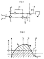
- Figure 1 shows two internal terminals 1, 2 of the portable data carrier, which are connected via a switch 3 to the gate of an E2-PROM memory cell 4.
- the programming voltage Upp can be present at the connection terminal 1 and the erase voltage at the connection terminal 2, for example.
- the programming voltage U pp which is connected via a switch 5 to the drain connection of the E 2 memory cell 4, can also be tapped at a further connection terminal 6.
- the source of the E2-PROM memory cell is connected to ground.
- the drain connection of the E2-PROM memory cell 4 is connected to an externally accessible connecting terminal 12 via the load path of a MOSFET 7.
- the dashed line indicates the separation between the memory chip card and the outside world.
- the gate connection of the MOSFET 7 is connected to an internal connection terminal 8.
- the external connection terminal 12 can be, for example, a data output.
- a data output stage is shown schematically. This consists of the MOSFET 11, whose load path is connected between the terminal 12 and ground.
- the gate connection of the MOSFET 11 is connected to an internal connection terminal 10, to which, for example, a data signal can be applied.
- a MOSFET 9 is provided, the load path of which is connected between the ground and the gate connection of the MOSFET 11.
- the gate terminal of the MOSFET 9 is also connected to the internal terminal 8.
- the external data input / output device designated. 13 shows a pull-up resistor which is connected externally between a supply voltage terminal 14 and the connecting terminal 12. This is usually integrated in the external read / write station.
- FIG 2 the time course of the threshold voltage after a programming operation is shown with X in principle.
- the E2 memory cell is programmed.
- the memory cell is then erased during the time period t0 to t1.
- the memory cell is in the erased state.
- the memory cell is again written during the time t2 to t3.
- A is the evaluation voltage threshold.
- the abscissa shows the time course and the ordinate shows the value of the threshold voltage.
- the hatched area B shows the area in which the E2-PROM memory cell is deleted and area C the area within which the E2-PROM memory cell is programmed.
- the programming state of an E2-PROM memory cell of the floating gate type ie the threshold voltage after a programming operation, therefore has an exponential dependence on the programming time. This is caused by the field-supported tunnel current.
- Such curves can be shifted, flattened or flattened by shifting manufacturing parameters, by different construction of the memory cells or different process control.
- the basic relationship remains the same for almost all E2-PROM cells.
- the conductivity of the memory cells can always be changed characteristically in the area of short programming times due to comparatively small programming time differences.
- this characteristic can be determined and evaluated from the outside. If a logical "0" signal is present at connection 8, then MOSFETs 7 and 9 are blocked. This is the normal state of the data carrier in which no authenticity test takes place. During this time, the threshold voltage of the E2-PROM cell according to the invention can also be gradually shifted by applying suitable programming voltages.
- connection 8 If, on the other hand, there is a logical "1" at connection 8, the evaluation can be carried out within the authenticity check.
- a logic "1" at connection 8 makes MOSFET 9 conductive and MOSFET 11 blocking. As a result, data transmission can no longer take place.
- MOSFET 7 also becomes conductive and the drain connection of the E2-PROM memory cell 4 is connected to the external connection 12.
- the programming state of the E2-PROM memory cell 4 can now be determined via the drain voltage of the E2-PROM memory cell 4 by the external data input / output 15.
- the control means required within the data carrier for programming or deleting the E2-PROM memory cell are not shown.
- the controllable switch 3 connects the terminal 2 and thus ground to the gate of the E2-PROM memory cell 4.
- the controllable switch 5 switches the programming voltage U pp to the drain connection.
- the programming voltage U pp from terminal 1 is applied to the gate via the switch 3 and the controllable switch 5 is opened, so that OV are applied to the drain of the E2-PROM memory cell.
- the switch 5 is opened and a gate voltage between 0 and 3 volts is applied.
- An authenticity check can be based, for example, on the written state of the memory cell, for which a drain voltage close to 0 volts can be determined externally. If the E2-PROM cell 4 is erased for a certain duration, a characteristic drain voltage results, depending on the duration of the erasure process, which can be measured by the data input / output device 15. The dependency on the programming time can be easily checked if the total time is divided into short individual pulses of e.g. 10 to 100 ⁇ s duration divided and taps the respective voltage level at an external load resistor 13 in series to the E2-PROM cell 4 in the breaks. If after a few erase pulses the threshold voltage of the E2-PROM cell 4 approaches the gate read voltage, the drain voltage will shift easily measurable by the trigger threshold of the evaluation logic in the data input / output device 15 in accordance with the current voltage characteristic and the load resistance 13.
- this data input / output device 15 has an AD converter, a voltage change as a property of the memory cell 4 can also be determined directly.
- Intermediate levels or fluently changeable pulse numbers when changing the individual pulse duration are criteria for the fact that the tested data carrier was actually provided specifically for this test, ie for this application, and is therefore genuine.
- Different but nevertheless "real" data carriers can react with a given pulse duration of, for example, 10 ⁇ s after a few pulses or even not at all, for example if the internal programming voltage has a long rise time as dead time due to internal pulse shaping.
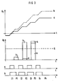
- Figure 3 illustrates an inventive process of the method.
- the four partial figures shown one above the other show courses of the threshold voltage UT and the drain voltage UD as a function of short pulses a and longer pulses b.
- the same time axis t applies to all sub-figures, that is to say that the temporal course of the four sub-figures shown corresponds in the vertical direction.
- short impulses are symbolically represented with a and longer impulses with I1, I2, I3, I4 in the bottom part with b.
- P1, P2, P3, P4 denote the interval pauses between the programming pulses.
- the uppermost part of the figure shows the dependency of the threshold voltage of the E2-PROM memory cell 4 with the solid curve for the short programming pulses a and with the dashed curve the course of the threshold voltage over time in the event that a programming pulse sequence according to the bottom part figure b is used .
- the middle figure shows the value of the drain voltage, which can be determined in the programming pauses P1, P2, P3, using bar graphs.
- the dashed line denotes a threshold Q. This can represent, for example, the decision criterion for a logical "0" or a logical "1".
- an AD converter could be provided on the data carrier directly between the memory cell and the data output. The characteristic size would then already be changed on the data carrier.
- a counter for counting the programming pulses could also be provided on the data carrier.
- E2-PROM-specific, analog test option is of course the defined change in the programming voltage and its characteristic influence on the programming curves.
- the current-voltage characteristics of the E2 which can be measured by the data input / output device and are dependent on the programming state can be measured -PROM memory cell can still be influenced by the data in the data memory, so that when the data content in the memory of the portable data carrier changes, the authenticity feature measured in an analog manner also changes characteristically.
- a special digital arithmetic unit can be preloaded using a simple algorithm before the authenticity test is carried out. This could, for example, be an exclusive OR network or a short feedback shift register.
- a network could be changed within the authenticity feature in such a way that either the programming process itself is influenced characteristically, ie is slowed down or accelerated, or the memory cell is evaluated with different current-voltage characteristic curves if the programming sequence is unchanged.
- the programming process of an E2-PROM memory cell can be accelerated or slowed down, for example, by changing the programming voltage or by changing a dead time, ie the rise time constant of the programming pulses.
- the evaluation can be influenced by changing the reading level or by connecting or disconnecting serial or parallel current paths to the E2-PROM cell.
- the drain voltage of which is determined during the authenticity check other memory cells or integrable components can of course also be used, which have a characteristic analog parameter that is difficult to simulate, for example, by DA converters.
Landscapes
- Engineering & Computer Science (AREA)
- General Physics & Mathematics (AREA)
- Physics & Mathematics (AREA)
- Business, Economics & Management (AREA)
- Microelectronics & Electronic Packaging (AREA)
- Theoretical Computer Science (AREA)
- Computer Security & Cryptography (AREA)
- Accounting & Taxation (AREA)
- Strategic Management (AREA)
- Computer Networks & Wireless Communication (AREA)
- General Business, Economics & Management (AREA)
- Computer Hardware Design (AREA)
- Read Only Memory (AREA)
- Credit Cards Or The Like (AREA)
Applications Claiming Priority (2)
| Application Number | Priority Date | Filing Date | Title |
|---|---|---|---|
| DE4242579 | 1992-12-16 | ||
| DE19924242579 DE4242579C2 (de) | 1992-12-16 | 1992-12-16 | Verfahren zur Echtheitserkennung von Datenträgern |
Publications (3)
| Publication Number | Publication Date |
|---|---|
| EP0602643A2 true EP0602643A2 (fr) | 1994-06-22 |
| EP0602643A3 EP0602643A3 (fr) | 1998-07-15 |
| EP0602643B1 EP0602643B1 (fr) | 2000-02-23 |
Family
ID=6475510
Family Applications (1)
| Application Number | Title | Priority Date | Filing Date |
|---|---|---|---|
| EP19930120325 Expired - Lifetime EP0602643B1 (fr) | 1992-12-16 | 1993-12-16 | Méthode et ensemble de support d'informations pour la reconnaissance de l'authenticité de la mémoire des puces |
Country Status (5)
| Country | Link |
|---|---|
| EP (1) | EP0602643B1 (fr) |
| DE (2) | DE4242579C2 (fr) |
| DK (1) | DK0602643T3 (fr) |
| ES (1) | ES2143486T3 (fr) |
| GR (1) | GR3033222T3 (fr) |
Cited By (4)
| Publication number | Priority date | Publication date | Assignee | Title |
|---|---|---|---|---|
| FR2764413A1 (fr) * | 1997-06-10 | 1998-12-11 | Sgs Thomson Microelectronics | Procede d'authentification de circuit integre |
| WO1999008230A2 (fr) | 1997-08-08 | 1999-02-18 | Infineon Technologies Ag | Procede pour verifier l'authenticite d'un support de donnees |
| WO2001052207A1 (fr) * | 2000-01-11 | 2001-07-19 | Infineon Technologies Ag | Microplaquette semi-conductrice d'identite univoque et procede de determination de l'identite univoque d'une microplaquette semi-conductrice |
| US7334307B1 (en) | 2006-05-23 | 2008-02-26 | Tomasz K Helenowski | Disposable set screw system |
Families Citing this family (3)
| Publication number | Priority date | Publication date | Assignee | Title |
|---|---|---|---|---|
| DE19913326A1 (de) * | 1999-03-24 | 2000-10-05 | Giesecke & Devrient Gmbh | Vorrichtung zur Prüfung der Echtheit eines tragbaren Datenträgers |
| DE19941682A1 (de) | 1999-09-01 | 2001-03-15 | Infineon Technologies Ag | Sicherheitsempfindliche Chipkarten |
| DE10041669A1 (de) * | 2000-08-10 | 2002-02-21 | Deutsche Telekom Ag | Verfahren und Vorrichtung zum Prüfen der Echtheit einer Chipkarte |
Family Cites Families (4)
| Publication number | Priority date | Publication date | Assignee | Title |
|---|---|---|---|---|
| US4931997A (en) * | 1987-03-16 | 1990-06-05 | Hitachi Ltd. | Semiconductor memory having storage buffer to save control data during bulk erase |
| DE3736882C2 (de) * | 1987-10-30 | 1997-04-30 | Gao Ges Automation Org | Verfahren zur Echtheitsprüfung eines Datenträgers mit integriertem Schaltkreis |
| ES2041772T3 (es) * | 1987-12-17 | 1993-12-01 | Siemens Aktiengesellschaft | Procedimiento y dispositivo de soporte de datos para el reconocimiento de la legitimidad de chips de memoria. |
| FR2640061B1 (fr) * | 1988-12-06 | 1992-04-10 | Schlumberger Ind Sa | Dispositif de lecture/ecriture de cartes a memoire muni d'un dispositif de detection de cartes simulees |
-
1992
- 1992-12-16 DE DE19924242579 patent/DE4242579C2/de not_active Expired - Fee Related
-
1993
- 1993-12-16 ES ES93120325T patent/ES2143486T3/es not_active Expired - Lifetime
- 1993-12-16 DE DE59309958T patent/DE59309958D1/de not_active Expired - Fee Related
- 1993-12-16 EP EP19930120325 patent/EP0602643B1/fr not_active Expired - Lifetime
- 1993-12-16 DK DK93120325T patent/DK0602643T3/da active
-
2000
- 2000-04-14 GR GR20000400913T patent/GR3033222T3/el not_active IP Right Cessation
Cited By (7)
| Publication number | Priority date | Publication date | Assignee | Title |
|---|---|---|---|---|
| FR2764413A1 (fr) * | 1997-06-10 | 1998-12-11 | Sgs Thomson Microelectronics | Procede d'authentification de circuit integre |
| EP0884704A1 (fr) * | 1997-06-10 | 1998-12-16 | STMicroelectronics S.A. | Procédé d'authentification de circuit intégré |
| US6848049B1 (en) | 1997-06-10 | 2005-01-25 | Stmicroelectronics S.A. | Method and apparatus for the authentication of integrated circuits |
| WO1999008230A2 (fr) | 1997-08-08 | 1999-02-18 | Infineon Technologies Ag | Procede pour verifier l'authenticite d'un support de donnees |
| US6615351B1 (en) | 1997-08-08 | 2003-09-02 | Infineon Technologies Ag | Method for checking the authenticity of a data medium |
| WO2001052207A1 (fr) * | 2000-01-11 | 2001-07-19 | Infineon Technologies Ag | Microplaquette semi-conductrice d'identite univoque et procede de determination de l'identite univoque d'une microplaquette semi-conductrice |
| US7334307B1 (en) | 2006-05-23 | 2008-02-26 | Tomasz K Helenowski | Disposable set screw system |
Also Published As
| Publication number | Publication date |
|---|---|
| DK0602643T3 (da) | 2000-07-24 |
| DE4242579C2 (de) | 1997-08-21 |
| DE59309958D1 (de) | 2000-03-30 |
| EP0602643A3 (fr) | 1998-07-15 |
| GR3033222T3 (en) | 2000-08-31 |
| EP0602643B1 (fr) | 2000-02-23 |
| DE4242579A1 (de) | 1994-06-23 |
| ES2143486T3 (es) | 2000-05-16 |
Similar Documents
| Publication | Publication Date | Title |
|---|---|---|
| DE2439577C2 (de) | Verfahren zum Prüfen von hochintegrierten logischen Schaltungen und Einrichtung zur Durchführung des Verfahrens | |
| DE3736882C2 (de) | Verfahren zur Echtheitsprüfung eines Datenträgers mit integriertem Schaltkreis | |
| DE69514790T2 (de) | Verfahren zur Einstellung der Schwellspannung einer Referenzspeicherzelle | |
| DE3936676C2 (fr) | ||
| DE602004008456T2 (de) | Integrierte ladungsleseschaltung für resistive speicher | |
| DE60317768T2 (de) | Verfahren zum Auslesen einer nichtflüchtigen Speichervorrichtung und zugehörige Vorrichtung | |
| DE69615736T2 (de) | Speicherkarte und Vorrichtung zum Betrieb einer solchen Karte | |
| DE102004059411B4 (de) | Flash-Speichervorrichtung und Verfahren zur Steuerung derselben | |
| DE4206286C2 (de) | Speicherzugriffssystem und Verfahren zum Ausgeben eines digitalen Datenstromes | |
| DE4005462A1 (de) | Zaehlverfahren und zaehlvorrichtung mit permanentspeicher | |
| EP0268106A2 (fr) | Système pour effectuer des transactions sans argent liquide | |
| DE19849560C2 (de) | Ausgangspufferschaltung zum Steuern einer Anstiegsrate | |
| DE69100120T2 (de) | Ultrahochgeschwindigkeitsspeicher mit Drainspannungsbegrenzer für Zellen. | |
| DE2514582C2 (de) | Schaltung zur erzeugung von leseimpulsen | |
| DE69218053T2 (de) | Speicherkarte zur Zählung von Daten und Lesevorrichtung | |
| DE69014821T2 (de) | Nichtflüchtige Speicheranordung. | |
| DE69029634T2 (de) | Prüflatchschaltung | |
| EP0123177B1 (fr) | Méthode et appareil pour commander une mémoire non volatile écriture/lecture d'utilisation | |
| EP0602643B1 (fr) | Méthode et ensemble de support d'informations pour la reconnaissance de l'authenticité de la mémoire des puces | |
| DE4042161C2 (fr) | ||
| DE69700156T2 (de) | Serieller Zugriffsspeicher mit Schreibsicherung | |
| DE2251640A1 (de) | Elektronisches speicherelement und dieses verwendendes speicherwerk | |
| DE69820080T2 (de) | Verfahren zum schreiben von binären datenwörtern mittels elektrisch-programmierbarer und löschbarer speicherzellen | |
| EP0321728B1 (fr) | Méthode et disposition de support de données pour l'authentification d'une carte à mémoire | |
| DE2525097C3 (de) | Verfahren zum Betrieb eines n-Kanal-Speicher-FET |
Legal Events
| Date | Code | Title | Description |
|---|---|---|---|
| PUAI | Public reference made under article 153(3) epc to a published international application that has entered the european phase |
Free format text: ORIGINAL CODE: 0009012 |
|
| AK | Designated contracting states |
Kind code of ref document: A2 Designated state(s): DE DK ES FR GB GR IT LU NL |
|
| PUAL | Search report despatched |
Free format text: ORIGINAL CODE: 0009013 |
|
| AK | Designated contracting states |
Kind code of ref document: A3 Designated state(s): DE DK ES FR GB GR IT LU NL |
|
| 17P | Request for examination filed |
Effective date: 19980805 |
|
| 17Q | First examination report despatched |
Effective date: 19990311 |
|
| GRAG | Despatch of communication of intention to grant |
Free format text: ORIGINAL CODE: EPIDOS AGRA |
|
| GRAG | Despatch of communication of intention to grant |
Free format text: ORIGINAL CODE: EPIDOS AGRA |
|
| GRAH | Despatch of communication of intention to grant a patent |
Free format text: ORIGINAL CODE: EPIDOS IGRA |
|
| GRAH | Despatch of communication of intention to grant a patent |
Free format text: ORIGINAL CODE: EPIDOS IGRA |
|
| GRAA | (expected) grant |
Free format text: ORIGINAL CODE: 0009210 |
|
| AK | Designated contracting states |
Kind code of ref document: B1 Designated state(s): DE DK ES FR GB GR IT LU NL |
|
| REF | Corresponds to: |
Ref document number: 59309958 Country of ref document: DE Date of ref document: 20000330 |
|
| ITF | It: translation for a ep patent filed | ||
| REG | Reference to a national code |
Ref country code: ES Ref legal event code: FG2A Ref document number: 2143486 Country of ref document: ES Kind code of ref document: T3 |
|
| GBT | Gb: translation of ep patent filed (gb section 77(6)(a)/1977) |
Effective date: 20000502 |
|
| ET | Fr: translation filed | ||
| REG | Reference to a national code |
Ref country code: DK Ref legal event code: T3 |
|
| PLBE | No opposition filed within time limit |
Free format text: ORIGINAL CODE: 0009261 |
|
| STAA | Information on the status of an ep patent application or granted ep patent |
Free format text: STATUS: NO OPPOSITION FILED WITHIN TIME LIMIT |
|
| 26N | No opposition filed | ||
| PGFP | Annual fee paid to national office [announced via postgrant information from national office to epo] |
Ref country code: GR Payment date: 20011130 Year of fee payment: 9 |
|
| PGFP | Annual fee paid to national office [announced via postgrant information from national office to epo] |
Ref country code: FR Payment date: 20011204 Year of fee payment: 9 |
|
| PGFP | Annual fee paid to national office [announced via postgrant information from national office to epo] |
Ref country code: DK Payment date: 20011206 Year of fee payment: 9 Ref country code: NL Payment date: 20011206 Year of fee payment: 9 Ref country code: GB Payment date: 20011206 Year of fee payment: 9 |
|
| PGFP | Annual fee paid to national office [announced via postgrant information from national office to epo] |
Ref country code: LU Payment date: 20011210 Year of fee payment: 9 |
|
| PGFP | Annual fee paid to national office [announced via postgrant information from national office to epo] |
Ref country code: ES Payment date: 20011213 Year of fee payment: 9 |
|
| REG | Reference to a national code |
Ref country code: GB Ref legal event code: IF02 |
|
| PGFP | Annual fee paid to national office [announced via postgrant information from national office to epo] |
Ref country code: DE Payment date: 20020218 Year of fee payment: 9 |
|
| PG25 | Lapsed in a contracting state [announced via postgrant information from national office to epo] |
Ref country code: LU Free format text: LAPSE BECAUSE OF NON-PAYMENT OF DUE FEES Effective date: 20021216 Ref country code: GB Free format text: LAPSE BECAUSE OF NON-PAYMENT OF DUE FEES Effective date: 20021216 |
|
| PG25 | Lapsed in a contracting state [announced via postgrant information from national office to epo] |
Ref country code: ES Free format text: LAPSE BECAUSE OF NON-PAYMENT OF DUE FEES Effective date: 20021217 |
|
| PG25 | Lapsed in a contracting state [announced via postgrant information from national office to epo] |
Ref country code: DK Free format text: LAPSE BECAUSE OF NON-PAYMENT OF DUE FEES Effective date: 20030131 |
|
| PG25 | Lapsed in a contracting state [announced via postgrant information from national office to epo] |
Ref country code: NL Free format text: LAPSE BECAUSE OF NON-PAYMENT OF DUE FEES Effective date: 20030701 Ref country code: DE Free format text: LAPSE BECAUSE OF NON-PAYMENT OF DUE FEES Effective date: 20030701 |
|
| PG25 | Lapsed in a contracting state [announced via postgrant information from national office to epo] |
Ref country code: GR Free format text: LAPSE BECAUSE OF NON-PAYMENT OF DUE FEES Effective date: 20030707 |
|
| REG | Reference to a national code |
Ref country code: DK Ref legal event code: EBP |
|
| GBPC | Gb: european patent ceased through non-payment of renewal fee |
Effective date: 20021216 |
|
| NLV4 | Nl: lapsed or anulled due to non-payment of the annual fee |
Effective date: 20030701 |
|
| PG25 | Lapsed in a contracting state [announced via postgrant information from national office to epo] |
Ref country code: FR Free format text: LAPSE BECAUSE OF NON-PAYMENT OF DUE FEES Effective date: 20030901 |
|
| REG | Reference to a national code |
Ref country code: FR Ref legal event code: ST |
|
| REG | Reference to a national code |
Ref country code: ES Ref legal event code: FD2A Effective date: 20021217 |
|
| PG25 | Lapsed in a contracting state [announced via postgrant information from national office to epo] |
Ref country code: IT Free format text: LAPSE BECAUSE OF NON-PAYMENT OF DUE FEES;WARNING: LAPSES OF ITALIAN PATENTS WITH EFFECTIVE DATE BEFORE 2007 MAY HAVE OCCURRED AT ANY TIME BEFORE 2007. THE CORRECT EFFECTIVE DATE MAY BE DIFFERENT FROM THE ONE RECORDED. Effective date: 20051216 |