EP0602723B1 - Circuit intégré comportant un paramètre ajustable électriquement - Google Patents
Circuit intégré comportant un paramètre ajustable électriquement Download PDFInfo
- Publication number
- EP0602723B1 EP0602723B1 EP93203454A EP93203454A EP0602723B1 EP 0602723 B1 EP0602723 B1 EP 0602723B1 EP 93203454 A EP93203454 A EP 93203454A EP 93203454 A EP93203454 A EP 93203454A EP 0602723 B1 EP0602723 B1 EP 0602723B1
- Authority
- EP
- European Patent Office
- Prior art keywords
- circuit
- current
- admittance
- transistor
- control signal
- Prior art date
- Legal status (The legal status is an assumption and is not a legal conclusion. Google has not performed a legal analysis and makes no representation as to the accuracy of the status listed.)
- Expired - Lifetime
Links
Images




Classifications
-
- H—ELECTRICITY
- H03—ELECTRONIC CIRCUITRY
- H03H—IMPEDANCE NETWORKS, e.g. RESONANT CIRCUITS; RESONATORS
- H03H11/00—Networks using active elements
- H03H11/46—One-port networks
Definitions
- the invention relates to an integrated circuit comprising adjusting means for adjusting at least one electronic parameter of the integrated circuit, the adjusting means being arranged for adjusting an effective admittance value of an effective admittance circuit comprising
- the invention also relates to an electronic circuit containing such an integrated circuit.
- a circuit with adjustable admittance is known from US patent No. 4,109,214.
- This publication describes the parallel circuit as a differential pair, with a first and second transistor whose emitters are connected to each other and to a DC current source.
- the admittance element for example a capacitor, is connected between the collector and the emitter of the first transistor.
- the first terminal is connected to the collector of the first transistor.
- the collector of the second transistor is coupled to the second terminal, which for AC purposes may be regarded as circuit ground.
- the emitter connection will have a low effective impedance to ground; this means that for the purpose of determining the current through the admittance element this element may be regarded as connected between the first and second terminal.
- the effective admittance has an admittance value which can be adjusted by controlling the conduction through the first and second transistor.
- the effective admittance value can be adjusted between zero admittance (in case the first transistor is made completely conductive and the second transistor is made non-conductive) and the admittance of the admittance element (in case the first transistor is made non conductive and the second transistor is made completely conductive).
- the conduction through the first and second transistor (and with it the effective admittance) is controlled by the difference between the voltages on the base connections of the first and second transistor.
- the effective admittance value depends exponentially upon this difference.
- the prior art teaches a control circuit which is coupled between the input for the control signal M and the base connection, and which realizes a linear relation between the effective admittance value and the control signal M.
- the adjustment of the effective admittance is often used in order to adjust an electronic parameter of the circuit other than the effective admittance itself.
- the linear relation between the effective admittance value and the control signal M does not guarantee a linear relation between the control signal M and the electronic parameter.
- Y ref is the admittance of the admittance element.
- the first term on the right corresponds to the current drawn by the admittance element, the second term corresponds to the proportional parallel current I p that is forcibly supplied in parallel to it by the parallel circuit.
- the second factor (the denominator) in the ratio f 1 /f 2 the depends on the control signal M makes it possible to realize a linear relationship between the control signal M and the electronic parameter for various cases.
- the restriction that the coefficient ⁇ is non-linearly dependent on the control signal M means that a/b is not equal to c/d.
- the dependence of the coefficient ⁇ on the control signal M may be substituted in the expression for the effective admittance value Y eff .
- Y eff Y ref c-a + ( d-b ) M c + dM
- the effective admittance value depends on the control signal M as a ratio of two factors which each depend linearly on the control signal M.
- the numerator will be constant.
- the effective admittance value depends inversely linearly from the control signal M: the effective impedance (which is the inverse of the effective admittance) depends linearly on the control signal M.
- the parallel circuit comprises a differential pair of a first and second transistor with their emitters coupled to each other, the admittance element being coupled in parallel to a collector emitter path of the first transistor,
- the first and second junction have mutually different junction areas.
- the linear dependence of f 2 on the control signal M may be set by means relative dimensioning of junction areas. These relative dimensions can be very accurately controlled in modern IC processes.
- the sum of the current densities may now be set to a linear function of the control signal M by using currents through the junctions which have mutually complementary linear dependence on the control signal M (i.e. whose sum is independent of the control signal M).
- Such a mutually complementary dependence can be realized in ways which are robust against spread in integrated circuit manufacturing parameters.
- the control circuit comprises current signal forming means, for forming a first and second current signal in dependence on the control signal M, the first and second current signals having a mutual difference which is linearly dependent on the control signal M, the control circuit comprising first and second current multiplying circuits, arranged for multiplying the first and second current signals with mutually unequal multiplication coefficients, and for supplying the multiplied first and second current signal to the first and second junction respectively.
- the control signal M dependence of the sum of the current densities is realized by supplying multiplied currents, whose sum is dependent on the control signal M, to the junctions.
- the current multiplying circuits may for example be realized using a first and second current mirror.
- the multiplication coefficients are differentiated by adjusting the relative emitter areas of the transistors in these current mirrors.
- the circuit with only the collector of first transistor and (AC) ground terminals of the effective admittance is a single ended circuit, because the current between the terminals will not depend on voltage changes at the second terminal (ground for AC purposes).
- An embodiment of the circuit according to the invention in which a collector of the first and second transistor are respectively coupled to a first and second terminal, the integrated circuit comprises
- adjustable double ended admittance circuits as such are known from European patent application No 0 225 332. This publication, however, does not address manipulation of the way in which the admittance depends on the control signal M.
- An embodiment of the integrated circuit according to the invention is characterized, in that the admittance element is coupled to the emitter of the first transistor via a current mirror, the admittance element being coupled to an input of the current mirror, an output of the current mirror being coupled to the emitter of the first transistor.
- the range over which the effective admittance value can be adjusted may be extended by a suitable choice of the amplification factor of the current mirror.
- a capacitor may be used as admittance element; this results in a adjustable effective capacitance value between the first and second terminal.
- the circuit may use internal capacitor in the integrated circuit, but it may also provide for connecting an external capacitor to add to any internal capacitance.
- An electronic circuit containing the integrated circuit according to the invention contains an oscillator comprising a negative resistance circuit coupled to a tank circuit, the tank circuit comprising an inductor and the effective admittance between the first and second terminal, the admittance element being a capactance, whereby an oscillating frequency of the oscillator circuit has a dependence on the control signal M, said dependence having zero second order derivative with respect to the control signal M at at least one point within an operative range of the control signal.
- the inductor will normally be provided as a discrete component connected to, but outside the integrated circuit.
- a zero second derivative (for an operative value of the control signal M for which the first derivative is not zero) is possible only because there is a suitable non-linear relation between the effective capacitance and the control signal M.
- An embodiment of the electronic circuit according to the invention is characterized, in that the inductor is a further admittance element in a further effective admittance, the tank circuit comprising the further effective admittance and further adjusting means, for adjusting an effective inductance of the further effective admittance under control of the control signal M, whereby the effective inductance and the effective admittance have a substantially identical dependence on the control signal M provided respectively by the further adjusting means and the adjusting means.
- the oscillation frequency f (which is proportional to (L eff C eff ) -1/2 , the inverse of the root of the product of the effective inductance L eff and the effective capacitance C eff ) can be made to have a dependence on the control signal M which does not contain a root, preferably a linear dependence.
- Figure 1 shows a circuit 10 for adjusting an effective admittance between an output terminal 11 and circuit ground (not shown).
- the circuit 10 has an input 17 for a control signal M, connected to a control circuit 19.
- the control circuit 19 has an output connected to a control input 12 of a current multiplying circuit 14.
- the current multiplying circuit 14 has a current input 15 and a current output 16.
- the current output 16 is connected to the output terminal 11.
- the current input 15 and the current output 16 are connected via an admittance element 18, which may for example be a capacitance, a resistor, an inductor or combinations thereof.
- a voltage V (with respect to a common reference level for the circuit, conventionally referred to as ground) is supplied to the output terminal 11.
- the sign of the input and output current is defined such that the input current is positive when it flows into input 15 of the current multiplying circuit 14 and the output current is positive when it flows out of the output 16 of the current multiplying circuit.
- the current multiplying coefficient a is defined such that it would be 1 if the current multiplying circuit were a direct connection between the current input 15 and output 16).
- the current I ref through the admittance element 18 flows into the current input 15 of the current multiplying element 15.
- the input admittance of the current input 15 is infinite.
- the first term on the right corresponds to the current drawn from the output 11 by the admittance element 18; the second term corresponds to the current delivered by the current multiplying circuit 14.
- an ideal current multiplying circuit 14 is assumed, that is, it is assumed that the input admittance Y in of the current input 15 is infinite, and that the output admittance Y out of the current output 16 is zero. In practice, this will not be the case.
- the formula above should then be corrected, replacing Y ref with the series arrangement of Y ref and Y in and replacing Y eff with the parallel arrangement of Y eff and Y out . However, in most cases the values of these admittances may be chosen such that this correction can be neglected.
- the multiplication coefficient ⁇ is controlled by the control signal M via the control circuit 19.
- Figure 2 shows a bipolar embodiment of the control circuit 19 and a bipolar embodiment of the current multiplying circuit 14.
- the control circuit 19 has an input 17 for the control signal M.
- the input 17 is connected to control two controllable current sources 440, 442 linearly.
- the first controllable current source 440 is connected to a first diode 420.
- the second controllable current source 442 is connected to a second diode 422.
- the diodes 420, 422 are shown as transistors with their collectors connected to their bases and to each other.
- the collectors of the transistors 420, 422 are connected to the power supply V p via a load 424.
- the output of the control circuit 19 is formed by the emitters of the first and second diodes 420, 422. Instead of transistors 420, 422, ordinary diodes may be used.
- the current multiplying circuit 14 contains a differential pair of a first and a second transistor 410, 412 with their emitters 411 connected to each other.
- the connection of the emitters 411 is connected to ground via a current source 416.
- the collectors of the first and second transistor are connected to the power supply V p via a load circuit 414, shown as a resistor 414a between the collector of the first transistor and the supply V p .
- the connection of the emitters 411 forms the current input 15, the collector of the first transistor forms the current output 16 of the current multiplying circuit 14.
- the control input 12a, 12b of the current multiplying circuit 14 is formed by the bases of the first and second transistor 410, 412.
- the base of the first transistor 410 in the current multiplying circuit 14 is connected to the emitter of the first diode 420 in the control circuit 19.
- the base of the second transistor 412 in the current multiplying circuit 14 is connected to the emitter of the second diode 422 in the control circuit 19.
- the current supplied to the current input 15 will flow in part through the collector emitter channel of the first transistor 410 of the current multiplying circuit 14. The remaining part flows through the second transistor 412. The part that flows through the first transistor 410 is forcibly delivered at the current output 16.
- the current multiplication coefficient a corresponds to the fraction of the input current that flows through the first transistor 410. This fraction is under control of the control circuit 19.
- the difference between the base-emitter voltages of the first and the second diodes 420, 422 in the control circuit 19 is equal to the difference between the base emitter voltages of the first and second transistor 410, 412 in the current multiplying circuit 14.
- the current multiplication coefficient a is the ratio of the current I 410 through the first transistor 410 and the sum of the currents I 410 , I 412 through the first and second transistors 410, 412. This ratio can be expressed in the currents through the diodes 420, 422 using the formula above.
- the current multiplication coefficient is ⁇ equal to a ratio f 1 /f 2 of two factors, where the second factor f 2 depends linearly on the control signal M.
- this is realized by controlling the first and second controllable current source 440, 442 separately to generate a first current I 420 for the first diode 420 and into a second current I 422 for the second diode 422.
- the control parameters a, b, c, d are chosen such that the sum of the two currents is dependent on the control signal M (d is not zero) and that the two dependencies are not strictly proportional to each other (a/c is not equal to b/d).
- the current multiplication factor ⁇ is a ratio of two factors f 1 /f 2 , the factor f 2 in the denominator depending linearly in the control signal M.
- the factor f 1 in the numerator may be kept constant or may also be made a linear function of the control signal M. In this way, it is possible to control the effective admittance value Y eff of the circuit inversely linear with the control signal M.
- Figure 3 shows how a similar dependence may be realized using any current amplifier 131 with a gain control input.
- the output of a multiplier and division circuit 135 is connected to the gain control input. This multiplier and division circuit 135 circuit will carry at its output the ratio of the signals presented at its inputs is coupled.
- the current amplifier may be realized for example as a voltage amplifier 132, provided with a current to voltage convertor 133 and a voltage to current converter 134 at its input and output respectively.
- the multiplier and division circuit 135 may be implemented with a two input multiplier 136 with a feedback amplifier 137 between its output and one of its inputs.
- one factor f 2 is supplied to a first one of the inputs 139 of the multiplier 136.
- the signal at the second input which is connected to the feedback amplifier 137, is regulated by this amplifier such that the output signal of the two input multiplier 136 is equal to the other factor f 1 .
- the signal value at the second input will be the ratio f 1 /f 2 which can be used to control the amplifier 131 via its gain control input. This achieves the same effect as the much more compact circuit of Figure 2.
- Both the input for fl 138 and f2 138 may moreover be provided with a polynomial computation circuit, (comprised of multiplication circuits and adding/ subtracting circuits) for cumputing polynomial functions of the control signal M.
- a polynomial computation circuit (comprised of multiplication circuits and adding/ subtracting circuits) for cumputing polynomial functions of the control signal M.
- Y eff Y ref c-a + ( d-b ) M c + dM
- the effective impedance that is, the inverse of the effective admittance Y eff
- the effective impedance is made a linear function (c+dM)/(ca)Y ref of the control signal M.
- the effective admittance by way of example a capacitor 21 of the circuit 10 is placed in series with a further admittance 20 having an admittance value Y f .
- the denominator will be made independent of the control signal M.
- the process by which the series admittance is linearized can be elucidated mathematically by modelling the effective admittance Y eff of the circuit 10 as a series arrangement of a control signal M independent series admittance (having an admittance Y ser ) and a linearly control signal M dependent admittance (having an admittance Y lin ).
- the admittance of a capacitor is proportional to its capacitance value. Therefore, when the admittance element is a capacitance, it can be modeled as a series arrangement of a control signal M independent series capacitance C ser and a linearly control signal M dependent admittance C lin .
- Figure 5 shows an example of an oscillating circuit, comprising a negative impedance element 30, connected to a tank circuit 32.
- the tank circuit contains a parallel arrangement of an inductor 34 and a capacitance circuit, in this case implemented as the parallel arrangement of a capacitor 36 and the circuit 10 of Figure 1.
- This LC circuit is a representative example: similar problems concerning linear adjustment apply to many well known LC oscillator structures).
- the combination of the negative impedance element 30 containing for example a feedback amplifier
- control signal M will need to change the oscillating frequency linearly if only over a small range.
- the relation between the effective capacitance C eff and the control signal M is linear
- the first derivative of the capacitance C eff with respect to the control signal M is not zero and the second derivative of the capacitance C eff with respect to the control signal M is zero.
- the first term on the left hand side of the equation above is zero and the second term is not zero. Therefore with a linear relation between the capacitance value and the control signal M an inflexion point cannot be realized.
- Non-linear control of the capacitance value makes it possible to introduce an inflexion point in the dependence of the oscillating frequency on the control signal M for the oscillator circuit shown in Figure 5.
- the adjusted capacitance may be modelled as a serial arrangement of a linearly variable capacitance C lin and a constant capacitance C ser .
- the inflexion point can be set to the desired nominal oscillating frequency and for a selected value of the control signal M.
- This circuit contains the negative resistance element 30 and a tank circuit 32. In the tank circuit, both the inductor and the capacitor are adjusted. For this purpose, the tank circuit 32 has an input 17 for a control signal M of two admittance adjusting circuits 510 and 520.
- the input 517 is coupled to a first control circuit 519, which has an output connected to a control input 512 of a first current multiplying circuit 514.
- the current input 515 and the current multiplying output 516 of the first current multiplying circuit 514 are connected via a first admittance element: an inductor 518.
- the input 517 is coupled to a second control circuit 529, which has an output connected to a control input 522 of a second current multiplying circuit 524.
- the current input 525 and the current multiplying output 526 of the second current multiplying circuit 524 are connected via a second admittance element: a capacitance 528.
- Both the output terminal 511, 521 of the first and second admittance adjusting circuit 510, 520 are connected to the tank circuit 32.
- L and C are the inductance and capacitance value respectively of the inductor 518 and the capacitor 528 used as admittance element in the first and second admittance adjusting circuit 510, 520, ⁇ is the angular frequency on which the admittance values depend.
- the invention is not limited to the simple LC circuit shown in Figure 5.
- Various further inductances and capacitances may be included in the negative resistance element 32 or in the connection between the admittance adjustment circuits 510, 520. Any effect of such inductances and capacitances on the linearity of frequency control can be compensated by a suitable choice of parameters in the adjusting circuits, in the same way as the effect of a serial capacitance upon the capacitance value can be eliminated.
- the control circuit 19 may be implemented in various ways.
- a first embodiment of the control circuit 19 is shown in Figure 7 as circuit 619. This circuit is similar to the control circuit shown in Figure 2. However, the controllable current sources 440, 442 have been replaced, by a first and second input transistor 60, 62.
- the input for the control signal M 617 is coupled to the base of the second input transistor 62 and via an inverting amplifier 64 to the base of the first input transistor 60.
- the emitters of the first and second input transistor are coupled to ground respectively via a first and a second resistor 66, 68.
- the collectors of the first and second input transistor are coupled to the emitters of respectively the first and second diode 620, 622, which are the equivalent of the diodes 420, 422 of Figure 2.
- Additional current sources 67, 69 are connected to the collector of the first and second input transistor.
- the control signal M is supplied as a voltage on the input 617 for the control signal M.
- the value of the resistors 66, 68 may be used to adjust the parameters b, d.
- the amplification factor s 64 of the amplifier 64 may be used to change the sign of b/d-1.
- FIG. 8 A second embodiment of the control circuit 19 is shown in Figure 8. This circuit is also similar to the control circuit of Figure 2.
- the controllable current sources 440, 442 have been replaced, by a first and second input transistor 70, 72, which have their emitters coupled via a resistor 73. The emitters are connected to ground via respective current sources 74, 75. These transistors constitute a differential amplifier, their bases forming the respective terminals 717a, 717b of a differential input.
- the collector of the first input transistor 70 is connected to the emitter of the first diode 720.
- the collector of the second input transistor 72 is connected to the emitter of the second diode 722.
- Two additional diodes 76, 77 are arranged in parallel to the first diode 720.
- the control signal M is supplied as a voltage difference V diff , supplied between the bases of the first and second input transistor 70, 72.
- the sum of the collector currents I 70 , I 72 of the first and second input transistor 70, 72 is independent of the difference voltage V diff and equal to the sum of the currents I 74 , I 75 produced by the current sources 74, 75.
- the fraction N may be controlled by using a single transistor 720 instead of the three transistors 720, 76, 77.
- the advantage of using emitter areas for adjusting the parameters a, b, c, d is that the important ratios between these parameters, such as b/d can be realized very accurately. This is because relative areas of transistors can be controlled to better than 1 part in 1000 in manufacturing the transistors on an integrated circuit.
- Figure 9 shows an example of an alternative control circuit.
- This circuit has two inputs 80, 81 for currents, each having its own linear dependencies on the control signal M (such currents may for example generated using an equivalent of part 70, 72, 73, 74, 75 of the circuit shown in Figure 8, such that the sum of the input currents is independent of the control signal M).
- the inputs are connected to the control inputs of respective current mirror circuits 82, 84.
- the outputs 86, 88 of the current mirror circuits are coupled to the diodes 420, 422 shown earlier.
- the current mirrors 82, 84 have mutually different current amplification factors, which are realized by using transistors with mutually different emitter areas (shown symbolically by drawing the output transistor of the current mirrors as a triple transistor).
- the ratio N' between the current multiplication factors of the current mirrors 82, 84 influences the current multiplication coefficient ⁇ in the same way as the area ratio A 720 /A 722 of the first and second diode 720, 722.
- the diodes 420, 422 can be arranged in several ways.
- the circuit in this Figure contains two controllable current sources 90, 92. (These current sources may be similar to those shown in Figures 7, 8, 9).
- the controllable current sources are respectively coupled to the collectors of two diodes (94, 95, 96, 98) shown as transistors, the first of which is shown as a threefold transistor to symbolize that it has a larger emitter area than the second transistor.
- the collector of the first transistor 94, 95, 96 is coupled to its base.
- the collector of the second transistor 98 is coupled to its base.
- the emitters of the first and second transistors 94, 95, 96, 98 are coupled to each other and via a current source 99 to ground.
- the bases serve as output for the control circuit (and are coupled to the bases of the first and second transistor 410, 412 of the current multiplying circuit 14, not shown).
- the circuit is arranged to ensure that the voltage difference between the outputs of the control circuit corresponds to the difference between the base emitter voltages of the diodes. This difference is in response to the currents supplied to the collectors of the diodes. Therefore the current multiplying coefficient is similarly controlled as in the circuit of Figure 2.
- the diode coupled transistors 420, 422, 94, 95, 96, 98 may also be replaced by ordinary junction diodes.
- Various other circuits may be used for generating a difference between two voltages across junctions and supplying this difference across the bases of the transistors 410, 412 of the differential pair. For example, one might use the circuit disclosed in US patent no 4,109,214, with the modification that the difference between the emitter voltages is taken from transistors with mutually different emitter areas.
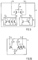
- Figure 11 shows an alternative current multiplying circuit 14. Instead of a resistor connected to the collector of the first transistor 410, a current mirror 100 is used with its input coupled to the collector of the second transistor 412 of the current multiplying circuit 14. The output of the current mirror 100 is coupled to the collector of the first transistor 410.
- Figure 12 shows a further modification of the current multiplying circuit 14.
- the current input 15 is connected to the input of a current mirror 110.
- the output of this current mirror is connected to the common connection of the emitters of the first and second transistor 410, 412.
- the output transistor of the current mirror 110 is shown as a double transistor, to symbolize that its emitter area may differ from that of the input transistor of the current mirror 110.
- the current mirror 110 will supply an output current to the common connection of the emitters of the first and second transistor 410, 412. This output current is a multiple of the current the input of the current mirror 110.
- the current multiplication factor between input and output will be ⁇ .
- the extra factor ⁇ gives an additional opportunity to adjust the effective admittance.
- the extra factor ⁇ has the additional advantage that it makes it possible for provide effective admittance values Y eff which are larger than the admittance value Y ref of the admittance element 18. Something which is not possible with the circuit of Figure 2. This may be of interest especially when the admittance element is an integrated capacitance.
- Figure 13 shows a symmetric circuit with an adjustable effective admittance.
- the circuit is similar to that of Figure 2, except that it has a symmetric current multiplying circuit.
- This multiplying circuit contains a first and second transistor pair.
- the first transistor pair contains a first and second transistor 122a, 124a, with their emitters mutually connected.
- the bases of the first and second transistor 122a, 124a are coupled to the emitters of a third and fourth transistor 420, 422, which are used as diodes.
- the second transistor pair contains a fifth and sixth transistor 122b, 124b, with their emitters mutually connected.
- the bases of first and second the transistor 122a, 124a are coupled to the respective bases of the fifth and sixth transistor 122b, 124b in the further pair.
- the collectors of the first and second transistor 122a, 124a are connected to the collectors of the sixth and fifth transistors 122b, 124b respectively. In this way the collectors and bases of the pairs are connected (122a, 124a) (122b, 124b), but the base and collector of each transistor are connected to mutually different transistors.
- the current multiplying circuit has two current inputs 125a, 125b, connected respectively to the common emitter connection of the first and second transistor 122a, 124a, and to the common emitter connection of the fifth and sixth transistor 122b, 124b.
- the current multiplying circuit has two current outputs 126a, 126b, coupled to the collectors of the first and second transistor 122a, 124b respectively.
- the circuit contains two admittance elements 128a, 128b each coupled between a current output 126a, 126b and a corresponding current input 125a, 125b.
- the circuit has two output terminals 120a, 120b, coupled to the two current outputs 126a, 126b.
- the circuit function is similar to that of the circuit shown in Figure 2.
- the sum of any changes in the current drawn from the two outputs 120a, 120b in response to a voltage supplied to these outputs is zero.
- the circuit draws a purely differential current.
- the admittance values Y 128a , Y 128b of the admittance elements 128a, 128b are equal, the circuit behaves as a two ended effective admittance. This is in contrast to the circuit shown in Figures 1 and 4, which show a single ended effective admittance, that is an admittance which has one of its terminals of the admittance connected to ground.
- the current changes in proportion to changes in the voltage difference applied between the two output terminals 120a, 120b.
- the proportionality constant, the effective admittance Y eff is the same as that for the single ended circuit.
- the double ended admittance has the advantage that there is no net current from the output terminal to ground in response to the applied voltages. This reduces interference problems. When the double ended circuit is used in an oscillator in an integrated circuit other circuits will be less interfered with due to ground currents.
- Figure 14 shows simulation results, for a double ended version of a practical oscillating circuit shown in Figure 5.
- An inductor 34 of 30.5 nH was used in parallel with a capacitor 36 of 2.7pF.
- the variable capacitor 10 was composed of a series arrangement of a 8.8pF capacitor and a adjustable capacitance created with a circuit according to Figure 13, with a control circuit according to Figure 8.
- the two admittance elements 128a, 128b were capacitors of 2.8pF.
- a ratio of 3:1 was used for the emitter areas of the transistors 420, 422.
- the oscillations frequency was thus approximately 480 Mhz.
- Figure 14 shows a graph in which the control signal M is plotted horizontally, and the oscillation frequency 141 and its derivative 142 with respect to the control signal M is plotted vertically.
- the vertical scales are offset: the baseline corresponds to a frequency and derivative greater than zero.
- the derivative is shown on a greatly expanded scale: its full vertical range corresponds to a change of derivative of approximately 1%. In the graph, the derivative changes slope; the point where its slope is zero corresponds to the inflexion point: the second order derivative is zero at this point.
- the control circuit 19 contains four diodes 151a-d between its outputs 12a,b. Midway between the outputs 12a,b there is a junction point 154 which is connected to a reference voltage V r . This junction point 154 is connected via two diodes 151a,b in the forward direction to one output 12a, and via two further diodes 151c,d in the forward direction to the other output 12b. Furthermore, the control circuit 19 contains four current sources 152a-d, connected to the respective outputs 12a,b and further junction points 155a,b between the outputs 12a,b and the junction point 154. All current sources 152a-d are coupled to receive the control signal M.
- the current sources 152a-d serve to provide a linear control of the current through the individual diodes 151a-d.
- the relation between the current multiplication coefficient ⁇ and the control signal M can be made a ratio of two quadratic polynomials.
- the relation between the effective admittance Y eff and the control signal M can be made the ratio of two quadratic polynomials.
- an application is a resonance circuit.
- an inductance L is connected to the output 11 of the admittance modulating circuit of figure 1, and a capacitance is used as reference admittance 18.
- the resonance frequency of this circuit varies as the inverse root of the capacitance.
- the resonance frequency of the resonance circuit can be made to depend linearly on the control signal M.
- the inductance of the resonance circuit will always be accompanied by parasitic capacitance.
- the effect of such a capacitance on the linearity of the relation between the resonance frequency and the control signal can always be compensated by an appropriate choice of the relation between the current densities through the various diodes 151a-d.
- I d I 0 ( a + M - 1)
- the effect of other parasitic components such as series capacitances may be compensated
Landscapes
- Networks Using Active Elements (AREA)
- Control Of Amplification And Gain Control (AREA)
Claims (9)
- Circuit intégré comprenant des moyens de réglage pour régler au moins un paramètre électronique du circuit intégré, les moyens de réglage étant à même de régler une valeur d'admittance effective d'un circuit à admittance effective comprenant :les moyens de réglage comprenant :un élément à admittance (18, 128a, 528),un circuit parallèle (14), couplé en parallèle à l'élément à admittance, et à même de conduire un courant parallèle Ip en parallèle à un courant traversant l'élément à admittance,caractérisé en ce que le circuit parallèle est à même de rendre le courant parallèle Ip proportionnel à un courant de référence Iref traversant l'élément à admittance : Ip = αIref, avec un coefficient de proportionnalité α, le circuit de commande étant à même d'établir le coefficient a dans une dépendance non linéaire à l'égard du signal de commande M, la dépendance étant un rapport f1/f2 d'un premier et d'un deuxième facteurs, dont le deuxième facteur f2 dépend sensiblement de manière polynomiale du signal de commande M.un circuit de commande (19), ayant une sortie (12) couplée à une entrée de commande du circuit parallèle et une entrée (17) pour un signal de commande M destiné à commander la conduction du circuit parallèle,
- Circuit intégré suivant la revendication 1,le circuit parallèle comprenant une paire différentielle d'un premier (410, 122a) et d'un deuxième (412, 124a) transistors, dont les émetteurs (411) sont couplés l'un à l'autre, l'élément à admittance étant couplé en parallèle à un trajet collecteur-émetteur du premier transistor,le circuit de commande comprenant une première (420) et une deuxième (422) jonctions de semi-conducteurs, le circuit de commande étant à même de commander les courants traversant les première et deuxième jonctions en fonction du signal de commande M, le circuit de commande étant à même de fournir, entre les bases respectives du premier et deuxième transistors, une tension correspondant à une somme de tensions apparaissant dans des polarités mutuellement opposées aux bornes de la première et de la deuxième jonctions, respectivement, caractérisé en ce que le circuit de commande est à même de former une somme d'une première et d'une deuxième densités de courants i1, i2 dans, respectivement, la première et la deuxième jonctions linéairement dépendante du signal de commande M, la première densité de courant étant pondérée dans ladite somme par un rapport d'aires d'émetteurs A1, A2, respectivement du premier et du deuxième transistors : i1A1/A2+i2.
- Circuit intégré suivant la revendication 2, les aires d'émetteurs A1, A2 du premier et du deuxième transistors étant sensiblement égales, caractérisé en ce que la première et la deuxième jonctions ont des aires de jonctions mutuellement différentes.
- Circuit intégré suivant la revendication 2 ou 3, caractérisé en ce que le circuit de commande comprend des moyens de formation de signaux de courants pour former un premier et un deuxième signaux de courants en fonction du signal de commande M, les premier et deuxième signaux de courants ayant une différence mutuelle qui est une fonction linéaire du signal de commande M, le circuit de commande comprenant des premier et deuxième circuits de multiplication de courants à même de multiplier les premier et deuxième signaux de courants par des coefficients de multiplication mutuellement inégaux, et à même de fournir les premier et deuxième signaux de courants multipliés aux première et deuxième jonctions, respectivement.
- Circuit intégré suivant la revendication 1, 2, 3 ou 4,le circuit parallèle comprenant une paire différentielle d'un premier et d'un deuxième transistors, dont les émetteurs sont couplés l'un à l'autre, l'élément à admittance étant couplé en parallèle à un trajet collecteur-émetteur du premier transistor,le circuit de commande comprenant une première et une deuxième jonctions de semi-conducteurs, le circuit de commande étant à même de commander les courants traversant les première et deuxième jonctions en fonction du signal de commande M, le circuit de commande étant à même de fournir, entre les bases respectives du premier et du deuxième transistors, une tension correspondant à une somme de tensions apparaissant dans des polarités mutuellement opposées aux bornes de la première et de la deuxième jonctions, respectivement, caractérisé en ce que le circuit de commande comprend au moins une troisième (76) et une quatrième (77) jonctions, la somme des tensions étant une somme de tensions apparaissant dans des polarités mutuellement opposées par paires aux bornes de la première et de la deuxième jonctions, et aux bornes de la troisième et de la quatrième jonctions, respectivement.
- Circuit intégré suivant la revendication 2, 3, 4 ou 5, dans lequel les collecteurs du premier (122a) et du deuxième (124a) transistors sont couplés respectivement à une première borne (120a) et à une deuxième borne (120b), le circuit intégré comprenant :une autre paire différentielle d'un cinquième (124b) et d'un sixième (122b) transistors, dont les émetteurs sont couplés l'un à l'autre, les collecteurs du cinquième et du sixième transistors étant respectivement couplés à une deuxième borne (120b) et à une première borne (120a),un autre élément à admittance (128b) couplé en parallèle à un trajet collecteur-émetteur du cinquième transistor,les connexions de bases du premier et du cinquième transistors étant connectées l'une à l'autre et les connexions de bases du deuxième et du sixième transistors étant connectées l'une à l'autre.
- Circuit intégré suivant l'une quelconque des revendications 2 à 6, caractérisé en ce que l'élément à admittance est couplé à l'émetteur du premier transistor via un miroir de courant (110), l'élément à admittance étant couplé à une entrée du miroir de courant, une sortie du miroir de courant étant couplée à l'émetteur du premier transistor.
- Circuit électronique comprenant le circuit intégré suivant l'une quelconque des revendications 1 à 7, le circuit électronique contenant un oscillateur comprenant un circuit à résistance négative (30) couplé à un circuit bouchon (32, 510, 520), le circuit bouchon comprenant une bobine d'inductance (34, 518) et l'admittance effective entre la première borne et la deuxième borne, l'élément à admittance étant un condensateur, de sorte qu'une fréquence d'oscillation du circuit oscillateur est une fonction du signal de commande M, ladite fonction ayant une dérivée seconde par rapport au signal de commande M nulle en au moins un point dans un domaine d'activité du signal de commande.
- Circuit électronique suivant la revendication 8, caractérisé en ce que la bobine d'inductance est un autre élément à admittance (518) dans une autre admittance effective (510), le circuit bouchon comprenant l'autre admittance effective et d'autres moyens de réglage (519) pour régler une inductance effective de l'autre admittance effective sous la commande du signal de commande M, de sorte que l'inductance effective et l'admittance effective (520) sont des fonctions sensiblement identiques du signal de commande M établies, respectivement, par les autres moyens de réglage et les moyens de réglage (529).
Applications Claiming Priority (2)
| Application Number | Priority Date | Filing Date | Title |
|---|---|---|---|
| EP92203925 | 1992-12-15 | ||
| EP92203925 | 1992-12-15 |
Publications (2)
| Publication Number | Publication Date |
|---|---|
| EP0602723A1 EP0602723A1 (fr) | 1994-06-22 |
| EP0602723B1 true EP0602723B1 (fr) | 1998-03-18 |
Family
ID=8211137
Family Applications (1)
| Application Number | Title | Priority Date | Filing Date |
|---|---|---|---|
| EP93203454A Expired - Lifetime EP0602723B1 (fr) | 1992-12-15 | 1993-12-09 | Circuit intégré comportant un paramètre ajustable électriquement |
Country Status (4)
| Country | Link |
|---|---|
| US (1) | US5578959A (fr) |
| EP (1) | EP0602723B1 (fr) |
| JP (1) | JPH06232689A (fr) |
| DE (1) | DE69317528T2 (fr) |
Families Citing this family (4)
| Publication number | Priority date | Publication date | Assignee | Title |
|---|---|---|---|---|
| DE4424527A1 (de) * | 1994-07-12 | 1996-01-18 | Philips Patentverwaltung | Schaltungsanordnung zur Kapazitätsverstärkung |
| US7199603B2 (en) | 2004-07-30 | 2007-04-03 | Microchip Technology Incorporated | Increment/decrement, chip select and selectable write to non-volatile memory using a two signal control protocol for an integrated circuit device |
| GB2442774A (en) * | 2006-10-12 | 2008-04-16 | Ericsson Telefon Ab L M | Electronically adjustable gain slope controller circuit |
| CN103123373A (zh) * | 2011-11-21 | 2013-05-29 | 鸿富锦精密工业(深圳)有限公司 | 电气参数测试装置 |
Family Cites Families (7)
| Publication number | Priority date | Publication date | Assignee | Title |
|---|---|---|---|---|
| US3571763A (en) * | 1968-02-05 | 1971-03-23 | Us Air Force | Immittance network incorporating one negative resistance |
| GB1573616A (en) * | 1976-03-04 | 1980-08-28 | Nat Semiconductor Uk Ltd | Electronic impedance devices |
| US4025867A (en) * | 1976-06-16 | 1977-05-24 | Bell Telephone Laboratories, Incorporated | Capacitance magnification circuit |
| US4109214A (en) * | 1977-05-31 | 1978-08-22 | Motorola, Inc. | Unbalanced-to-balanced signal converter circuit |
| US4602224A (en) * | 1984-12-20 | 1986-07-22 | Nippon Motorola Ltd. | Variable capacitance reactance circuit |
| US4638265A (en) * | 1985-06-03 | 1987-01-20 | Motorola, Inc. | Balanced variable reactance circuit and method of producing the same |
| JPS623515A (ja) * | 1985-06-29 | 1987-01-09 | Nec Corp | 電圧制御型可変容量回路 |
-
1993
- 1993-12-09 EP EP93203454A patent/EP0602723B1/fr not_active Expired - Lifetime
- 1993-12-09 DE DE69317528T patent/DE69317528T2/de not_active Expired - Fee Related
- 1993-12-13 JP JP5311999A patent/JPH06232689A/ja active Pending
- 1993-12-14 US US08/167,278 patent/US5578959A/en not_active Expired - Fee Related
Also Published As
| Publication number | Publication date |
|---|---|
| JPH06232689A (ja) | 1994-08-19 |
| DE69317528D1 (de) | 1998-04-23 |
| DE69317528T2 (de) | 1998-09-10 |
| EP0602723A1 (fr) | 1994-06-22 |
| US5578959A (en) | 1996-11-26 |
Similar Documents
| Publication | Publication Date | Title |
|---|---|---|
| FI108585B (fi) | Taajuusviritysjärjestelmä OTA-C-parille | |
| JPH08293758A (ja) | モノリシックhbt式能動同調可能帯域フィルタ | |
| KR920006292B1 (ko) | 제어가능한 적분기 | |
| US5192884A (en) | Active filter having reduced capacitor area but maintaining filter characteristics | |
| JPH0846483A (ja) | キャパシタンス増大用回路配置 | |
| US6411170B2 (en) | Oscillation circuit | |
| EP0602723B1 (fr) | Circuit intégré comportant un paramètre ajustable électriquement | |
| JPH01161904A (ja) | 移相発振器 | |
| US6621331B2 (en) | Variable negative resistance cell for bipolar integrated circuits | |
| US5028884A (en) | Leapfrog filter having adjustable center frequency and quality factor | |
| US5648741A (en) | Circuit having overall transfer function providing temperature compensation | |
| US20040041669A1 (en) | Tuning circuit | |
| EP1510001B1 (fr) | Circuit amplificateur, circuit giratoire, dispositif de filtrage et procede pour amplifier un signal | |
| GB2230155A (en) | Voltage-controlled current source | |
| US6329870B1 (en) | Reference voltage generating circuitry | |
| JPH0671190B2 (ja) | 集積可変容量性リアクタンス回路 | |
| JP2507010B2 (ja) | フィルタ回路 | |
| JP2991727B2 (ja) | アクティブフィルタ回路 | |
| JP2753031B2 (ja) | 発振回路 | |
| KR940004744B1 (ko) | 가변임피던스회로 | |
| JP2841563B2 (ja) | 可変インピーダンス回路 | |
| JP2901248B2 (ja) | 可変リアクタンス回路 | |
| Sotner et al. | Design adaptation of an electronically tunable oscillator using a low performance linearized CMOS operational transconductance amplifier | |
| Khan | Digitally programmable tuned circuits | |
| JP2895300B2 (ja) | 定遅延フィルタ |
Legal Events
| Date | Code | Title | Description |
|---|---|---|---|
| PUAI | Public reference made under article 153(3) epc to a published international application that has entered the european phase |
Free format text: ORIGINAL CODE: 0009012 |
|
| AK | Designated contracting states |
Kind code of ref document: A1 Designated state(s): DE FR GB IT |
|
| RAP1 | Party data changed (applicant data changed or rights of an application transferred) |
Owner name: N.V. PHILIPS' GLOEILAMPENFABRIEKEN |
|
| 17P | Request for examination filed |
Effective date: 19941222 |
|
| GRAG | Despatch of communication of intention to grant |
Free format text: ORIGINAL CODE: EPIDOS AGRA |
|
| 17Q | First examination report despatched |
Effective date: 19970325 |
|
| GRAG | Despatch of communication of intention to grant |
Free format text: ORIGINAL CODE: EPIDOS AGRA |
|
| GRAH | Despatch of communication of intention to grant a patent |
Free format text: ORIGINAL CODE: EPIDOS IGRA |
|
| GRAH | Despatch of communication of intention to grant a patent |
Free format text: ORIGINAL CODE: EPIDOS IGRA |
|
| GRAA | (expected) grant |
Free format text: ORIGINAL CODE: 0009210 |
|
| AK | Designated contracting states |
Kind code of ref document: B1 Designated state(s): DE FR GB IT |
|
| PG25 | Lapsed in a contracting state [announced via postgrant information from national office to epo] |
Ref country code: IT Free format text: LAPSE BECAUSE OF FAILURE TO SUBMIT A TRANSLATION OF THE DESCRIPTION OR TO PAY THE FEE WITHIN THE PRE;WARNING: LAPSES OF ITALIAN PATENTS WITH EFFECTIVE DATE BEFORE 2007 MAY HAVE OCCURRED AT ANY TIME BEFORE 2007. THE CORRECT EFFECTIVE DATE MAY BE DIFFERENT FROM THE ONE RECORDED.SCRIBED TIME-LIMIT Effective date: 19980318 |
|
| REF | Corresponds to: |
Ref document number: 69317528 Country of ref document: DE Date of ref document: 19980423 |
|
| ET | Fr: translation filed | ||
| RAP4 | Party data changed (patent owner data changed or rights of a patent transferred) |
Owner name: KONINKLIJKE PHILIPS ELECTRONICS N.V. |
|
| REG | Reference to a national code |
Ref country code: FR Ref legal event code: CD |
|
| PLBE | No opposition filed within time limit |
Free format text: ORIGINAL CODE: 0009261 |
|
| 26N | No opposition filed | ||
| PGFP | Annual fee paid to national office [announced via postgrant information from national office to epo] |
Ref country code: GB Payment date: 20001220 Year of fee payment: 8 |
|
| PGFP | Annual fee paid to national office [announced via postgrant information from national office to epo] |
Ref country code: FR Payment date: 20001226 Year of fee payment: 8 |
|
| PGFP | Annual fee paid to national office [announced via postgrant information from national office to epo] |
Ref country code: DE Payment date: 20010214 Year of fee payment: 8 |
|
| PG25 | Lapsed in a contracting state [announced via postgrant information from national office to epo] |
Ref country code: GB Free format text: LAPSE BECAUSE OF NON-PAYMENT OF DUE FEES Effective date: 20011209 |
|
| REG | Reference to a national code |
Ref country code: GB Ref legal event code: IF02 |
|
| PG25 | Lapsed in a contracting state [announced via postgrant information from national office to epo] |
Ref country code: DE Free format text: LAPSE BECAUSE OF NON-PAYMENT OF DUE FEES Effective date: 20020702 |
|
| GBPC | Gb: european patent ceased through non-payment of renewal fee |
Effective date: 20011209 |
|
| PG25 | Lapsed in a contracting state [announced via postgrant information from national office to epo] |
Ref country code: FR Free format text: LAPSE BECAUSE OF NON-PAYMENT OF DUE FEES Effective date: 20020830 |
|
| REG | Reference to a national code |
Ref country code: FR Ref legal event code: ST |