EP0602872A2 - Formation de rayon avec optique de diffraction binaire - Google Patents
Formation de rayon avec optique de diffraction binaire Download PDFInfo
- Publication number
- EP0602872A2 EP0602872A2 EP93309795A EP93309795A EP0602872A2 EP 0602872 A2 EP0602872 A2 EP 0602872A2 EP 93309795 A EP93309795 A EP 93309795A EP 93309795 A EP93309795 A EP 93309795A EP 0602872 A2 EP0602872 A2 EP 0602872A2
- Authority
- EP
- European Patent Office
- Prior art keywords
- light beam
- binary diffraction
- intensity
- optic lens
- diffraction optic
- Prior art date
- Legal status (The legal status is an assumption and is not a legal conclusion. Google has not performed a legal analysis and makes no representation as to the accuracy of the status listed.)
- Ceased
Links
- 230000007423 decrease Effects 0.000 claims description 3
- 230000003287 optical effect Effects 0.000 abstract description 11
- 239000013078 crystal Substances 0.000 description 25
- 230000003247 decreasing effect Effects 0.000 description 3
- 230000000694 effects Effects 0.000 description 3
- XEEYBQQBJWHFJM-UHFFFAOYSA-N Iron Chemical compound [Fe] XEEYBQQBJWHFJM-UHFFFAOYSA-N 0.000 description 2
- 239000000969 carrier Substances 0.000 description 2
- 238000010521 absorption reaction Methods 0.000 description 1
- 239000011248 coating agent Substances 0.000 description 1
- 238000000576 coating method Methods 0.000 description 1
- 230000001066 destructive effect Effects 0.000 description 1
- 230000006866 deterioration Effects 0.000 description 1
- 238000009792 diffusion process Methods 0.000 description 1
- 230000005684 electric field Effects 0.000 description 1
- 230000003090 exacerbative effect Effects 0.000 description 1
- 238000003384 imaging method Methods 0.000 description 1
- 239000012535 impurity Substances 0.000 description 1
- 229910052742 iron Inorganic materials 0.000 description 1
- GQYHUHYESMUTHG-UHFFFAOYSA-N lithium niobate Chemical compound [Li+].[O-][Nb](=O)=O GQYHUHYESMUTHG-UHFFFAOYSA-N 0.000 description 1
- 238000000034 method Methods 0.000 description 1
- 229920002120 photoresistant polymer Polymers 0.000 description 1
- 238000001020 plasma etching Methods 0.000 description 1
- 238000000992 sputter etching Methods 0.000 description 1
- 239000000758 substrate Substances 0.000 description 1
Images


Classifications
-
- G—PHYSICS
- G02—OPTICS
- G02B—OPTICAL ELEMENTS, SYSTEMS OR APPARATUS
- G02B27/00—Optical systems or apparatus not provided for by any of the groups G02B1/00 - G02B26/00, G02B30/00
- G02B27/42—Diffraction optics, i.e. systems including a diffractive element being designed for providing a diffractive effect
- G02B27/4205—Diffraction optics, i.e. systems including a diffractive element being designed for providing a diffractive effect having a diffractive optical element [DOE] contributing to image formation, e.g. whereby modulation transfer function MTF or optical aberrations are relevant
- G02B27/4227—Diffraction optics, i.e. systems including a diffractive element being designed for providing a diffractive effect having a diffractive optical element [DOE] contributing to image formation, e.g. whereby modulation transfer function MTF or optical aberrations are relevant in image scanning systems
-
- G—PHYSICS
- G02—OPTICS
- G02B—OPTICAL ELEMENTS, SYSTEMS OR APPARATUS
- G02B27/00—Optical systems or apparatus not provided for by any of the groups G02B1/00 - G02B26/00, G02B30/00
- G02B27/0025—Optical systems or apparatus not provided for by any of the groups G02B1/00 - G02B26/00, G02B30/00 for optical correction, e.g. distorsion, aberration
- G02B27/0037—Optical systems or apparatus not provided for by any of the groups G02B1/00 - G02B26/00, G02B30/00 for optical correction, e.g. distorsion, aberration with diffracting elements
-
- G—PHYSICS
- G02—OPTICS
- G02B—OPTICAL ELEMENTS, SYSTEMS OR APPARATUS
- G02B27/00—Optical systems or apparatus not provided for by any of the groups G02B1/00 - G02B26/00, G02B30/00
- G02B27/42—Diffraction optics, i.e. systems including a diffractive element being designed for providing a diffractive effect
- G02B27/4233—Diffraction optics, i.e. systems including a diffractive element being designed for providing a diffractive effect having a diffractive element [DOE] contributing to a non-imaging application
- G02B27/4244—Diffraction optics, i.e. systems including a diffractive element being designed for providing a diffractive effect having a diffractive element [DOE] contributing to a non-imaging application in wavelength selecting devices
-
- G—PHYSICS
- G02—OPTICS
- G02B—OPTICAL ELEMENTS, SYSTEMS OR APPARATUS
- G02B27/00—Optical systems or apparatus not provided for by any of the groups G02B1/00 - G02B26/00, G02B30/00
- G02B27/42—Diffraction optics, i.e. systems including a diffractive element being designed for providing a diffractive effect
- G02B27/4233—Diffraction optics, i.e. systems including a diffractive element being designed for providing a diffractive effect having a diffractive element [DOE] contributing to a non-imaging application
- G02B27/425—Diffraction optics, i.e. systems including a diffractive element being designed for providing a diffractive effect having a diffractive element [DOE] contributing to a non-imaging application in illumination systems
-
- G—PHYSICS
- G02—OPTICS
- G02B—OPTICAL ELEMENTS, SYSTEMS OR APPARATUS
- G02B27/00—Optical systems or apparatus not provided for by any of the groups G02B1/00 - G02B26/00, G02B30/00
- G02B27/42—Diffraction optics, i.e. systems including a diffractive element being designed for providing a diffractive effect
- G02B27/4272—Diffraction optics, i.e. systems including a diffractive element being designed for providing a diffractive effect having plural diffractive elements positioned sequentially along the optical path
- G02B27/4277—Diffraction optics, i.e. systems including a diffractive element being designed for providing a diffractive effect having plural diffractive elements positioned sequentially along the optical path being separated by an air space
-
- G—PHYSICS
- G02—OPTICS
- G02B—OPTICAL ELEMENTS, SYSTEMS OR APPARATUS
- G02B27/00—Optical systems or apparatus not provided for by any of the groups G02B1/00 - G02B26/00, G02B30/00
- G02B27/09—Beam shaping, e.g. changing the cross-sectional area, not otherwise provided for
- G02B27/0938—Using specific optical elements
- G02B27/0944—Diffractive optical elements, e.g. gratings, holograms
Definitions
- This invention relates to a raster scanner in which the intensity of a light beam is reprofiled across its width.
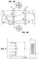
- a conventional raster scanner system utilizes a light source 12, a modulator 14, a multi-faceted rotating polygon mirror 16 as the scanning element and a photosensitive medium 18.
- the modulator 14 receives pixel information and modulates the light beam 20 in accordance with the pixel information.
- the raster scanner system utilizes overfill scanning and therefore, the modulated light beam 20 will be directed onto two facets 22 of the rotating polygon mirror 16.
- the rotating polygon mirror 16 reflects the light beam 20 and also causes the reflected light 20 to revolve about an axis near the center of rotation of the rotating polygon 16 and scans a line. This reflected light beam 20 can be utilized to impinge upon a photographic film or a photosensitive medium 18, such as a xerographic drum at the output of the imaging system.
- a laser light beam has a Gaussian distribution 30 which has a maximum intensity at the center C of the beam and a gradually decreasing intensity towards the outer shell S of the beam.
- an electro-optic crystal 14a used in the modulator 14 should be wide enough to encompass the width w of the light beam.
- the intensity of the light beam varies from the center C of the beam to the outer shell 5
- the surface of the electro-optic crystal 14a of the modulator 14 does not receive a uniform intensity.
- the center portion Ca of the electro-optic crystal is exposed to the maximum intensity from the center C of the light beam and the rest of the electro-optic crystal is exposed to less intensity.
- the non-uniform light excites carriers from impurities such as iron in the crystal. These carriers move in the crystal by diffusion and under the influence of electric fields are displaced to new positions and re-trapped, which results in specially varying refractive index changes due to the electro-optic effect.
- This phenomenon of index variation is called the "photorefractive effect” , or “optical damage” and is well documented in the literature. It is desirable in the case of information storage, but undesirable in the case of electro-optic modulator applications, since the index changes persist for long times and cause undesirable diffraction of light passing through the crystal. In particular the damage depends on the intensity of the light, which is not uniform in the case of a Gaussian beam.
- Readjustment of the modulator 14 can correct the performance of the center of the electro-optic crystal however, it over corrects the performance of the rest of the electro-optic crystal. Therefore, an electro-optic crystal, which is damaged only at the center, is no longer useful and it has to be replaced by a new electro-optic crystal.
- the uniform intensity can be applied to other optical applications such as multi-channel AO modulators, or indeed any optical system application, which requires a uniform optical beam.
- an overfilled raster scanning apparatus comprising a light source emitting a light beam; a binary diffraction optic lens system comprising a first binary diffraction optic lens and a second binary diffraction optic lens spaced along said light beam path from said first binary diffraction optic lens; said binary diffraction optic lens system being arranged to receive said light beam from said light source and reprofile the intensity of said light beam across its width; a photo sensitive medium; and a rotating scanning means arranged to receive said reprofiled light beam from said binary diffraction optic lens system and scan said light beam across said photo sensitive medium.
- a pair of binary diffraction optic lenses are utilized to change the intensity profile of a light beam to a uniform intensity profile.
- both binary diffraction optic lenses of this invention can be considered divided into an equal number of segments.
- Each segment of the first binary diffraction optic lens either diverges or converges a portion of a light beam and, as needed, deflects the same portion of the beam.
- Each segment of the second binary diffraction optic lens receives the light beam from a respective segment of the first binary diffraction optic lens and collimates the light beam. In application, the segments are so small that the intensity profile change is essentially continuous.
- a pair of binary diffraction optic lenses are utilized to change the intensity profile of a light beam from any profile to any desired profile.
- Both binary diffraction optic lenses of this invention have an equal number of segments. Depending on the shape of a desired intensity profile, each segment of the first binary diffraction optic lens either diverges or converges a portion of a light beam and, as needed, deflects the same portion of the beam.
- Each segment of the second binary diffraction optic lens receives the light beam from a respective segment of the first binary diffraction optic lens and collimates the light beam.
- FIG. 3 there is shown a typical beam with a Gaussian distribution 30 directed towards a facet of a rotating polygon mirror as in Figure 1.
- BDO binary diffraction optic
- the Gaussian distribution is divided into infinitesimal sections of equal energy bands 30a, 30b, 30c, 30d, 30e, 30f, 30g, 30h, 30i and 30j.
- Each one of the bands 30a, 30b, 30c, 30d, 30e, 30f, 30g, 30h, 30i and 30j has a width a, b, c, d, e, f, g, h, i and j respectively.
- the bands closer to the center of Gaussian distribution such as band 30e are narrower and have more intensity and the bands closer to the sides of the Gaussian distribution such as 30a are wider and have less intensity.
- the energy for all the bands is the same.
- the profile 50 which can have a width w equal to the width w of the Gaussian distribution 30, is divided into infinitesimal sections of equal energy bands 50a, 50b, 50c, 50d, 50e, 50f, 50g, 50h, 50i and 50j. Since the intensity of this profile 50 will be uniform, all bands 50a, 50b, 50c, 50d, 50e, 50f, 50g, 50h, 50i and 50h have equal widths n and contain the same energy.
- each one of the binary diffraction optic lenses 40 and 42 has to be designed to have a separate segment for each band. It should be noted that each segment has a plurality of infinitesimal stepped wedges (see Figures 4A and 4B).
- Each one of segments 40a, 40b, 40c, 40d, 40e, 40f, 40g, 40h, 40i and 40j is designed to convert the bands 30a, 30b, 30c, 30d, 30e, 30f, 30g, 30h, 30i and 30j into bands 50a, 50b, 50c, 50d, 50e, 50f, 50g, 50h, 50i and 50j respectively.
- each one of the segments 42a, 42b, 42c, 42d, 42e, 42f, 42g, 42h, 42i and 42j is designed to collimate each one of the bands 50a, 50b, 50c, 50d, 50e, 50f, 50g, 50h, 50i and 50j respectively.
- segment 40a of the BDO 40 has to be capable of receiving band 30a and converge it in such a manner that when the band 30a strikes a facet, it will have a narrower width n. Since the energy of each band is kept constant, the energy of band 50a will still be the same as band 30a. However, since the band 50a has a narrower width n and the energy is constant, the intensity increases. In other words, if a wide band of light is compressed into a narrower band the intensity of the narrower band increases.
- segment 40e of the BDO 40 has to be designed to be capable of receiving band 30e, diverging and, as needed, deflecting the band in such a manner that when it strikes a facet, it will have a wider width n. Since the width n is wider than width e and the energy is constant, the intensity decreases.
- Figure 4A shows a representative magnified exaggerated lower portion of segment 40a of Figure 3 and Figure 4B shows a representative magnified exaggerated upper portion of segment 40e of Figure 3.
- Figure 4A as the lower edge 37 of band 30a passes through the segment 40a and exits from one of the stepped wedges 41 of the segment 40a, it deflects.
- Figure 4B as the upper edge 39 of band 30e passes through the segment 40e and exits from one of the stepped wedges 43 of the segment 40e, it deflects.
- a uniform profile such as profile 50 improves the performance of an electro-optic modulator, which has a crystal 14.
- an electro-optic modulator crystal 14 has a beam profile 30 of uniform intensity, illuminating the active region of the modulator 14a, the electro-optic crystal is damaged uniformly in the active region 14a and due to the uniformity of the optical damage in the crystal, the index change is approximately uniform.
- the disclosed embodiment of this invention uses the light beam more efficiently since it allows utilization of a greater portion of the beam.
- Binary diffraction optic lenses are made using the same techniques used to fabricate VLSl circuits, as disclosed in Binary Optics Technology: The Theory and Design of Multi-level Diffractive Optical Elements by G.J. Swanson of the Lincoln Laboratory at the Massachusetts Institute of Technology, (Technical Report 854, 14 August 1989) and in US-A-4,895,790.
- a designer develops an idealized diffractive surface structure mathematically, then using a computer, defines a series of precise, microlithographic masks.
- a mask pattern is printed into a photoresist coating using a UV light source and then transferred into the optical substrate by ion milling or plasma etching.
- the BDO pair disclosed in the embodiment of this invention can be designed to reprofile any intensity profile of some given shape to any desirable intensity profile and can be used in any system which may need a certain intensity profile.
- Figures 6 and 7 illustrate the principal of this invention wherein two different intensity profiles are changed into desired profiles.
- Figure 6 changes the intensity profile 30 of Figure 3 to an intensity profile 64.
- Figure 7 changes an intensity profile 70 to an intensity profile 90.
- Figures 6 and 7 show only two of the unlimited possibilities of using this invention.
- the profile 64 which has a width w equal to the width w of the Gaussian distribution 30, has to be divided into infinitesimal sections of equal energy bands 64a, 64b, 64c, 64d, 64e, 64f, 64g, 64h, 64i and 64j.
- Each one of the bands 64a, 64b, 64c, 64d, 64e, 64f, 64g, 64h, 64i and 64j has a width a', b', c', d', e', f', g', h', i' and j' respectively.
- each one of the binary diffraction optic lenses 60 and 62 has to be designed to have a separate segment for each band.
- Each one of segments 60a, 60b, 60c, 60d, 60e, 60f, 60g, 60h, 60i and 60j is designed to convert the bands 30a, 30b, 30c, 30d, 30e, 30f, 30g, 30h, 30i and 30j into banos 64a, 64b, 64c, 64d, 64e, 64f, 64g, 64h, 64i and 64j respectively.
- each one of the segments 62a, 62b, 62c, 62d, 62e, 62f, 62g, 62h, 62i and 62j is designed to collimate each one of the bands 64a, 64b, 64c, 64d, 64e, 64f, 64g, 64h, 64i and 64j respectively.
- segment 60a of the BDO 60 has to be capable of receiving band 30a and converging it in such a manner that the band 30a will have a narrower width a' to achieve the intensity required. Since the band 30a has a narrower width a' at band 64a, the intensity increases. In other words, if a wide band of light is compressed into a narrower band the intensity of the narrower band increases.
- segment 60e of the BDO 60 has to be designed to be capable of receiving band 60e, diverging and deflecting, as needed, the band in such a manner that when it strikes a facet, it will have a wider width e' for the desired intensity decrease.
- a profile such as profile 64 is generated. It should be noted that depending on the desired profile, it might be necessary to have some segments of the BDO 60 to direct the bands through without diverging or converging the bands. Profile 64 has more intensity at one end and less intensity at the other end and a gradually decreasing intensity therebetween.
- each one of the binary diffraction optic lenses 80 and 82 has to be designed to have a separate segment for each band.
- Each one of segments 80a, 80b, 80c, 80d, 80e, 80f, 80g, 80h, 80i and 80j is designed to convert the bands 70a, 70b, 70c, 70d, 70e, 70f, 70g, 70h, 70i and 70j into bands 90a, 90b, 90c, 90d, 90e, 90f, 90g, 90h, 90i, and 90j respectively.
- each one of the segments 82a, 82b, 82c, 82d, 82e, 82f, 82g, 82h, 82i and 82j is designed to collimate each one of the bands 90a, 90b, 90c, 90d, 90e, 90f, 90g, 90h, 90i and 90j respectively.
Landscapes
- Physics & Mathematics (AREA)
- General Physics & Mathematics (AREA)
- Optics & Photonics (AREA)
- Spectroscopy & Molecular Physics (AREA)
- Mechanical Optical Scanning Systems (AREA)
- Facsimile Scanning Arrangements (AREA)
Applications Claiming Priority (2)
| Application Number | Priority Date | Filing Date | Title |
|---|---|---|---|
| US07/990,491 US5315427A (en) | 1992-12-14 | 1992-12-14 | Pair of binary diffraction optics for use in overfilled raster output scanning systems |
| US990491 | 1992-12-14 |
Publications (2)
| Publication Number | Publication Date |
|---|---|
| EP0602872A2 true EP0602872A2 (fr) | 1994-06-22 |
| EP0602872A3 EP0602872A3 (fr) | 1995-05-10 |
Family
ID=25536209
Family Applications (1)
| Application Number | Title | Priority Date | Filing Date |
|---|---|---|---|
| EP93309795A Ceased EP0602872A3 (fr) | 1992-12-14 | 1993-12-07 | Formation de rayon avec optique de diffraction binaire. |
Country Status (3)
| Country | Link |
|---|---|
| US (1) | US5315427A (fr) |
| EP (1) | EP0602872A3 (fr) |
| JP (1) | JPH06214184A (fr) |
Cited By (2)
| Publication number | Priority date | Publication date | Assignee | Title |
|---|---|---|---|---|
| EP0967508A3 (fr) * | 1998-06-23 | 2003-07-23 | Canon Kabushiki Kaisha | Dispositif optique de balayage |
| EP0848246B1 (fr) * | 1996-12-11 | 2006-03-08 | G.D Societ Per Azioni | Procédé de mesure de l'intensité d'un rayonnement transmis à travers un corps |
Families Citing this family (27)
| Publication number | Priority date | Publication date | Assignee | Title |
|---|---|---|---|---|
| US5422753A (en) * | 1993-12-23 | 1995-06-06 | Xerox Corporation | Binary diffraction optical element for controlling scanning beam intensity in a raster output scanning (ROS) optical system |
| US5610733A (en) * | 1994-02-28 | 1997-03-11 | Digital Optics Corporation | Beam-homogenizer |
| US5850300A (en) * | 1994-02-28 | 1998-12-15 | Digital Optics Corporation | Diffractive beam homogenizer having free-form fringes |
| US6392808B1 (en) | 1994-02-28 | 2002-05-21 | Digital Optics Corporation | Broad band controlled angle analog diffuser and associated methods |
| US5479583A (en) * | 1994-05-02 | 1995-12-26 | Xerox Corporation | Means to achieve a square intensity profile at an image plane by intensity and phase profiling |
| JP3104618B2 (ja) * | 1996-05-10 | 2000-10-30 | 富士ゼロックス株式会社 | 光学走査装置及び光学レンズ |
| US6008941A (en) * | 1996-06-25 | 1999-12-28 | Digital Optics Corporation | Optical soft aperture and use thereof |
| US5986807A (en) * | 1997-01-13 | 1999-11-16 | Xerox Corporation | Single binary optical element beam homogenizer |
| JPH11326804A (ja) * | 1998-03-16 | 1999-11-26 | Canon Inc | カラー画像形成装置及び走査光学装置 |
| AUPP446598A0 (en) * | 1998-07-03 | 1998-07-30 | Australian National University, The | Planar lightwave circuits |
| US6542304B2 (en) | 1999-05-17 | 2003-04-01 | Toolz, Ltd. | Laser beam device with apertured reflective element |
| US6341030B1 (en) | 1999-07-14 | 2002-01-22 | Minolta Co., Ltd. | Light beam optical scanner and image forming apparatus |
| US6313948B1 (en) * | 1999-08-02 | 2001-11-06 | James I. Hanna | Optical beam shaper |
| DE102004035489A1 (de) * | 2004-07-19 | 2006-02-16 | Jenoptik Laser, Optik, Systeme Gmbh | Optisches System zur Umwandlung einer primären Intensitätsverteilung in eine vorgegebene, raumwinkelabhängige Intensitätsverteilung |
| US7972776B2 (en) * | 2005-11-15 | 2011-07-05 | Oncohealth Corporation | Protein chips for HPV detection |
| US7732166B2 (en) * | 2005-11-15 | 2010-06-08 | Oncohealth Corporation | Detection method for human pappilomavirus (HPV) and its application in cervical cancer |
| US7569463B2 (en) * | 2006-03-08 | 2009-08-04 | Applied Materials, Inc. | Method of thermal processing structures formed on a substrate |
| US20080025354A1 (en) * | 2006-07-31 | 2008-01-31 | Dean Jennings | Ultra-Fast Beam Dithering with Surface Acoustic Wave Modulator |
| US7548364B2 (en) | 2006-07-31 | 2009-06-16 | Applied Materials, Inc. | Ultra-fast beam dithering with surface acoustic wave modulator |
| WO2010129821A1 (fr) | 2009-05-07 | 2010-11-11 | Oncohealth Corporation | Identification de grade élevée ou ≥cin2 pour détection, surveillance et diagnostic, à des stades précoces et des stades avancés, de papillomavirus humain (hpv) et de cancers associés au hpv |
| US8968995B2 (en) * | 2008-11-12 | 2015-03-03 | Oncohealth Corp. | Detection, screening, and diagnosis of HPV-associated cancers |
| US8278056B2 (en) * | 2008-06-13 | 2012-10-02 | Oncohealth Corp. | Detection of early stages and late stages HPV infection |
| US8148663B2 (en) * | 2007-07-31 | 2012-04-03 | Applied Materials, Inc. | Apparatus and method of improving beam shaping and beam homogenization |
| JP4943493B2 (ja) * | 2009-12-04 | 2012-05-30 | シャープ株式会社 | 光学走査装置及びそれを備えた画像形成装置 |
| JP5819851B2 (ja) | 2010-01-08 | 2015-11-24 | オンコヘルス コーポレーション | Hpv関連の癌の治療及びスクリーニングのための細胞に基づいた高処理能力hpv免疫アッセイ |
| US12210171B2 (en) | 2020-12-17 | 2025-01-28 | Waymo Llc | Combined collimation and diffuser lens for flood illuminator |
| US12085732B1 (en) | 2020-12-17 | 2024-09-10 | Waymo Llc | Combined collimation and diffuser lens for flood illuminator |
Citations (2)
| Publication number | Priority date | Publication date | Assignee | Title |
|---|---|---|---|---|
| US4895790A (en) * | 1987-09-21 | 1990-01-23 | Massachusetts Institute Of Technology | High-efficiency, multilevel, diffractive optical elements |
| EP0602870A2 (fr) * | 1992-12-14 | 1994-06-22 | Xerox Corporation | Illumination optimale d'une facette polygonale |
Family Cites Families (5)
| Publication number | Priority date | Publication date | Assignee | Title |
|---|---|---|---|---|
| US5138490A (en) * | 1989-04-29 | 1992-08-11 | Carl-Zeiss-Stiftung | Arrangement for changing the geometrical form of a light beam |
| US4941721A (en) * | 1989-06-01 | 1990-07-17 | Xerox Corporation | Raster scanning system utilizing overfilled polygon facet design |
| US5061025A (en) * | 1990-04-13 | 1991-10-29 | Eastman Kodak Company | Hologon scanner with beam shaping stationary diffraction grating |
| US5208701A (en) * | 1991-12-24 | 1993-05-04 | Xerox Corporation | Wobble correction lens with binary diffractive optic surface and refractive cylindrical surface |
| US5258862A (en) * | 1992-12-10 | 1993-11-02 | Xerox Corporation | Rotating disc optical synchronization system using binary diffractive optical elements |
-
1992
- 1992-12-14 US US07/990,491 patent/US5315427A/en not_active Expired - Fee Related
-
1993
- 1993-11-18 JP JP5289114A patent/JPH06214184A/ja active Pending
- 1993-12-07 EP EP93309795A patent/EP0602872A3/fr not_active Ceased
Patent Citations (2)
| Publication number | Priority date | Publication date | Assignee | Title |
|---|---|---|---|---|
| US4895790A (en) * | 1987-09-21 | 1990-01-23 | Massachusetts Institute Of Technology | High-efficiency, multilevel, diffractive optical elements |
| EP0602870A2 (fr) * | 1992-12-14 | 1994-06-22 | Xerox Corporation | Illumination optimale d'une facette polygonale |
Non-Patent Citations (1)
| Title |
|---|
| HAN C.Y., ISHII Y., MURATA K.: "Reshaping collimated laser beams with Gaussian profile to uniform profiles", APPLIED OPTICS, vol. 22, no. 22, 15 November 1983 (1983-11-15), pages 3644 - 3647, XP001092737, DOI: doi:10.1364/AO.22.003644 * |
Cited By (2)
| Publication number | Priority date | Publication date | Assignee | Title |
|---|---|---|---|---|
| EP0848246B1 (fr) * | 1996-12-11 | 2006-03-08 | G.D Societ Per Azioni | Procédé de mesure de l'intensité d'un rayonnement transmis à travers un corps |
| EP0967508A3 (fr) * | 1998-06-23 | 2003-07-23 | Canon Kabushiki Kaisha | Dispositif optique de balayage |
Also Published As
| Publication number | Publication date |
|---|---|
| EP0602872A3 (fr) | 1995-05-10 |
| US5315427A (en) | 1994-05-24 |
| JPH06214184A (ja) | 1994-08-05 |
Similar Documents
| Publication | Publication Date | Title |
|---|---|---|
| US5315427A (en) | Pair of binary diffraction optics for use in overfilled raster output scanning systems | |
| EP0660153B1 (fr) | Elément optique de diffraction binaire pour le contrÔle d'intensité pour un système optique de balayage ROS | |
| US6965465B2 (en) | Optical scanning apparatus and image forming apparatus using the same | |
| US8068265B2 (en) | Scanning optical apparatus | |
| US6064417A (en) | Laser printer using multiple sets of lasers with multiple wavelengths | |
| US3944323A (en) | Variable spot size scanning system | |
| US5331468A (en) | Intensity redistribution for exposure correction in an overfilled symmetrical laser printer | |
| US5111343A (en) | Gradient filter | |
| EP0602870A2 (fr) | Illumination optimale d'une facette polygonale | |
| EP0526846A2 (fr) | Appareil de balayage optique à plusieurs faisceaux | |
| JPH01210921A (ja) | 傾斜誤差及び走査湾曲誤差を補償できる電子写真プリンタ | |
| JP2781023B2 (ja) | 振動対策を施したros型印刷機 | |
| US4527858A (en) | Uniform speed scanning lens having a high resolving power | |
| JP2001215430A (ja) | 走査光学装置及びそれを用いた画像形成装置 | |
| JP2002221681A (ja) | 走査光学装置及びそれを用いた画像形成装置 | |
| KR100404408B1 (ko) | 광 주사 장치, 다중 비임 광 주사 장치 및 화상 형성 장치 | |
| US4536084A (en) | Projection device | |
| JPS622539A (ja) | 照明光学系 | |
| JP2001296491A (ja) | 光走査装置及びそれを用いた画像形成装置 | |
| EP0575988A1 (fr) | Système de balayage à miroir polygonal illuminé totalement d'une manière symmétrique | |
| EP0577405A1 (fr) | Correction de l'uniformité du balayage | |
| EP0681394B1 (fr) | Dispositif d'analyse de frame avec un profil d'intensité au carré sur un plan d'image | |
| US5969747A (en) | Efficient LED light geometry for optical printers | |
| JPH04212119A (ja) | 光走査装置 | |
| EP0695078B1 (fr) | Correction rapide de spot de balayage pour un polygone à balayage de trame |
Legal Events
| Date | Code | Title | Description |
|---|---|---|---|
| PUAI | Public reference made under article 153(3) epc to a published international application that has entered the european phase |
Free format text: ORIGINAL CODE: 0009012 |
|
| AK | Designated contracting states |
Kind code of ref document: A2 Designated state(s): DE FR GB IT |
|
| PUAL | Search report despatched |
Free format text: ORIGINAL CODE: 0009013 |
|
| AK | Designated contracting states |
Kind code of ref document: A3 Designated state(s): DE FR GB IT |
|
| 17P | Request for examination filed |
Effective date: 19951110 |
|
| 17Q | First examination report despatched |
Effective date: 19980113 |
|
| STAA | Information on the status of an ep patent application or granted ep patent |
Free format text: STATUS: THE APPLICATION HAS BEEN REFUSED |
|
| 18R | Application refused |
Effective date: 20020917 |