EP0602886B1 - Masque pour la sélection de composants multibit d'un opérande composé - Google Patents
Masque pour la sélection de composants multibit d'un opérande composé Download PDFInfo
- Publication number
- EP0602886B1 EP0602886B1 EP93309860A EP93309860A EP0602886B1 EP 0602886 B1 EP0602886 B1 EP 0602886B1 EP 93309860 A EP93309860 A EP 93309860A EP 93309860 A EP93309860 A EP 93309860A EP 0602886 B1 EP0602886 B1 EP 0602886B1
- Authority
- EP
- European Patent Office
- Prior art keywords
- operand
- bit
- data item
- mask
- component data
- Prior art date
- Legal status (The legal status is an assumption and is not a legal conclusion. Google has not performed a legal analysis and makes no representation as to the accuracy of the status listed.)
- Expired - Lifetime
Links
Images





Classifications
-
- G—PHYSICS
- G06—COMPUTING OR CALCULATING; COUNTING
- G06F—ELECTRIC DIGITAL DATA PROCESSING
- G06F7/00—Methods or arrangements for processing data by operating upon the order or content of the data handled
- G06F7/76—Arrangements for rearranging, permuting or selecting data according to predetermined rules, independently of the content of the data
- G06F7/764—Masking
-
- G—PHYSICS
- G06—COMPUTING OR CALCULATING; COUNTING
- G06F—ELECTRIC DIGITAL DATA PROCESSING
- G06F9/00—Arrangements for program control, e.g. control units
- G06F9/06—Arrangements for program control, e.g. control units using stored programs, i.e. using an internal store of processing equipment to receive or retain programs
- G06F9/30—Arrangements for executing machine instructions, e.g. instruction decode
- G06F9/30003—Arrangements for executing specific machine instructions
- G06F9/30007—Arrangements for executing specific machine instructions to perform operations on data operands
- G06F9/30036—Instructions to perform operations on packed data, e.g. vector, tile or matrix operations
-
- G—PHYSICS
- G06—COMPUTING OR CALCULATING; COUNTING
- G06F—ELECTRIC DIGITAL DATA PROCESSING
- G06F9/00—Arrangements for program control, e.g. control units
- G06F9/06—Arrangements for program control, e.g. control units using stored programs, i.e. using an internal store of processing equipment to receive or retain programs
- G06F9/30—Arrangements for executing machine instructions, e.g. instruction decode
- G06F9/30003—Arrangements for executing specific machine instructions
- G06F9/30007—Arrangements for executing specific machine instructions to perform operations on data operands
- G06F9/30036—Instructions to perform operations on packed data, e.g. vector, tile or matrix operations
- G06F9/30038—Instructions to perform operations on packed data, e.g. vector, tile or matrix operations using a mask
Definitions
- the present invention relates to techniques that perform operations selectively on plural data items.
- a mask is defined at col. 4 lines 59-64 as an image that contains substantially solid regions of ON pixels corresponding to regions of interest in an original image.
- a grayscale scanner can output multiple bits per pixel, and the grayscale scan can be binarized to produce a highlight image (HI).
- a highlight region (HR) mask can be produced from an HI by removing pixels from unhighlighted areas while retaining the highlighted regions in their entirety.
- the HR mask can be used in a variety of ways.
- Figs. 14C and 15C show examples of HR masks.
- the HR mask can be used with an inverse bit map of an HI to produce an highlight mark (HM) image including only those parts of the marks that are covered by the HR.
- FIG. 16 A first stage of specialized hardware in Fig. 16 is an array of bit-slice processors.
- Guttag et al., US-A-5,056,041 describe a bit mapped computer graphics environment. Bit-addressable operations on a wide data word of the bit mapped memory are carried out in that the process of writing CPU data to the memory is controlled.
- a mask data bus provides mask bits aligned with the data bits of the CPU to indicate the CPU data bits which are to be masked.
- CPU data is written into a plurality of latches at a time where the latches are isolated from the data bus.
- data on the data bus is selectively rewritten to those bit positions of the latch which are indicated by the mask bits. Finally the modified content of the latch is presented on the data bus and written into the memory.
- Fig. 7 shows a Connection Machine system that performs image processing by simulating a binary image jungle (BIJ).
- a front end processor can make calls to cause processing units in the Connection Machine to perform arithmetic and logical operations.
- Fig. 8 illustrates a part of an array of processing units in a Connection Machine, with a processing unit storing a pixel value.
- the section beginning at page 26 line 15 describes label propagation or labeling, stating that it is possible to select, or single out, all pixels labeled with similar values of a given property in parallel.
- the section beginning at page 28 line 3 describes selection, stating that selective processing can be achieved by first performing a selection operation to select a set of pixels labeled with similar values, and then performing processing on the selected set of pixels.
- a pixel can be selected by setting asingle bit label "on" in its processing unit.
- Fig. 24 illustrates general steps in applying a selection criterion using the low and high limits of a range of interest.
- Page 31, beginning at line 15, describes extensions to handle color and gray shaded images.
- the invention deals with a problem in processing multi-bit data items, such as gray scale or color pixel values.
- Operations on multi-bit data items are often conditional. An operation may be performed only on data items that meet a criterion, while other data items are not affected. Therefore, it is often necessary to operate selectively on data items.
- Masks can be produced and used as described by Bloomberg et al. '109, above. Selective processing can be performed as described by Mahoney.
- a single processor can typically operate on only one multi-bit data item at a time. This can be inefficient, especially if a processor is more than twice as wide as each multi-bit data item.
- the invention strives to provide improved techniques that operate in parallel on a subset of component data items within a composite operand that includes plural multi-bit component data items.
- the techniques use special operands, referred to herein as "mask operands.”
- the present invention provides a method of operating a processor and a system as set out in claims 1 and 13.
- One technique performs a logic operation in parallel on a mask operand and a composite operand to obtain a resulting operand that includes a subset of components from the composite operand.
- One or more operations can then be performed in parallel on the resulting operand. For example, a modified resulting data item can be obtained for each component in the subset and an unmodified resulting data item can be obtained for other components.
- Another technique performs logic operations in parallel on the mask operand, its inverse, and two composite operands to merge the composite operands.
- This technique can be implemented to merge a composite operand with modified resulting data items obtained as described above.
- the resulting operand is the same as the composite operand except that operations have been performed on selected components.
- This technique can also be used to merge two composite operands by selecting the maximum or minimum of each pair of aligned components.
- a mask operand can include a bit position for each bit position in a composite operand. In each bit position of one subset of components, the mask operand has a first value. In each bit position of another subset of components, the mask operand has a second value.
- a logic operation that obtains a resulting operand from a composite operand can preserve the composite operand where the mask operand has the first value but preserve the mask operand where the mask operand has the second value; an AND operation could be used if the first value is ON and the second is OFF, or an OR operation if the first value is OFF and the second is ON.
- logic operations that merge two composite operands can preserve one composite operand where the mask operand has the first value and preserve the other where the mask operand has the second value.
- a mask operand can be obtained in advance and stored for subsequent use. But it is often necessary to obtain a mask operand that distinguishes component data items that meet a criterion from components that do not. For example, it may be desirable to select only components that are or are not at least as great as a threshold, or that are equal or unequal to a constant, or that fall within or outside a range. In these situations, the mask operand cannot be obtained until the components among which it selects are available.
- Another aspect of the invention is based on the discovery of techniques that can obtain a mask operand using a composite operand that includes components among which the mask operand selects. These techniques make it possible to prepare a mask operand by operating in parallel on components between which the mask operand distinguishes.
- Techniques that prepare a mask operand can begin with a flag bit for each component data item in a composite operand.
- the flag bit indicates whether the component meets a criterion.
- the flag bit is positioned at or adjacent an end of the component within the composite operand.
- One technique can obtain a mask operand from a flag bit positioned at either end of a component data item.
- a logic operation is performed in parallel to select only the values of the flag bits to obtain a flag bit operand.
- the flag bit operand is shifted one bit and a logic operation is performed in parallel to propagate each flag bit to an adjacent bit position.
- two operations are performed per bit position, a shift operation and a logic operation. These operations are repeated until each flag bit has been propagated to every bit position of the respective component, producing a mask operand.
- Another technique can obtain a mask operand more rapidly from a flag bit positioned at the least significant bit of a component data item.
- a logic operation is performed in parallel to select only the values of the flag bits in a flag bit operand.
- an arithmetic operation is performed in parallel on the flag bit operand to obtain a mask. If each flag bit is obtained in the least significant bit position, only one arithmetic operation is required for this technique.
- each flag bit is obtained at or adjacent the most significant bit of its component, a shift operation is also required for each bit position; if the number of bit positions is greater than two, this technique is faster than the above technique that performs two operations for each bit position This technique can be even faster if special circuitry can be used to shift the flag bits more quickly to the least significant bit position.
- the techniques of the invention can be implemented in an article of manufacture.
- the article includes a data storage medium and instruction data stored by the data storage medium, which could be a magnetic storage medium, an optical storage medium, a semiconductor memory, or other memory medium.
- the article can be used in a system that includes memory, a storage medium access device, and a processor.
- the memory stores multi-bit data items.
- the instruction data indicate mask operand instructions a processor can execute to obtain a mask operand from a composite operand with plural multi-bit component data items or to perform a logic operation in parallel using a mask operand and a composite operand with plural multi-bit components.
- the mask operand includes a bit aligned with each bit in the composite operand. In each bit aligned with the bits of one subset of components, the mask operand has a first value. In each bit aligned with another subset of components, the mask operand has a second value.
- Mask operands can be used in various ways: An array of data items can be filtered by selecting only components above a threshold, equal to a constant, or within a range. Two arrays can be compared or merged using mask operands to select the maximum or minimum of each pair of components. Multiplication, division, and threshold convolution operations can be performed using mask operands More generally, any serial operation on multi-bit data items can be converted into an operation that can be performed by operating in parallel on composite operands that include plural multi-bit component data items.
- the techniques of the invention are advantageous because they permit efficient operations in parallel on multi-bit data items. Some of the techniques can be used to obtain a mask operand from a composite operand with plural multi-bit component data items, allowing branching and other conditional operations to be performed in parallel. Other techniques perform operations in parallel using a mask operand and one or more composite operands with plural multi-bit component data items. A wide variety of operations can be implemented using these techniques.
- Figs. 1-5 illustrate general features of the invention.
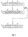
- Fig. 1 shows schematically how a composite operand can be used to obtain a mask operand which can be used to select a component data item from the composite operand.
- the term "composite operand" is an operand that includes two or more data items referred to as "component data items" or components.
- Fig. 2 shows a software product with instruction data indicating instructions a processor can perform in accordance with a technique like that in Fig. 1.
- Fig. 3 shows general acts in using a mask operand.
- Fig. 4 shows general acts in obtaining a mask operand.
- Fig. 5 shows general components of a processor that includes K-bit shifting circuitry for use in obtaining a mask operand.
- composite operand 10 includes component data items 12, 14, and 16, each including two bits.
- Component 12 has the value 11, component 14 the value 10, and component 16 the value 01.
- Mask operand 20 which can be produced from composite operand 10, is a filter in the sense that it selects only components in composite operand 10 that have values equal to 10. Therefore, mask operand has OFF in bit positions 22 aligned with component 12, ON in bit positions 24 aligned with component 14, and OFF in bit positions 26 aligned with component 16.
- result 30 includes resulting data items 32, 34, and 36.
- Data items 32 and 36 each include only zeros as a result of the AND operation because bit positions 22 and 26 are OFF, while data item 34 has the value 10 from component 14 because bit positions 24 are ON.
- Fig. 2 shows software product 60, an article of manufacture that can be used in a system that includes components like those shown in Fig. 2.
- Software product 60 includes data storage medium 62 that can be accessed by storage medium access device 64.
- Data storage medium 62 could, for example, be a magnetic medium such as a set of one or more floppy disks, an optical medium such as a set of one or more CD-ROMs, semiconductor memory, or any other appropriate medium for storing data.
- Data storage medium 62 stores data that storage medium access device 64 can provide to processor 66, which could for example be a microprocessor.
- Processor 66 is connected for receiving data from input circuitry 70.
- the data could be obtained from any appropriate source, such as a facsimile (fax) machine; a scanner, which could be the scanner of a digital copier or an input/output device of a computer; an editor, which could be a forms editor or other interactive image editor controlled by user input devices such as a keyboard and mouse or a pen- or stylus-based input device; or a network, which could be a local area network or other network capable of transmitting data.
- the data could relate to an image.
- Processor 66 is also connected for providing data to output circuitry 72.
- the data could in turn be provided to a fax machine, a printer, a display, or a network.
- the printer could be the printer of a digital copier or an input/output device of a computer.
- software product 60 includes data stored by storage medium 62.
- the stored data include instruction data indicating mask obtaining instructions 80 and mask using instructions 82.
- Processor 66 can execute instructions 80 to obtain a mask data item for each of plural component data items in a composite operand. The mask data items together form a mask operand.
- Processor 66 can execute instructions 82 to perform a logic operation on the composite operand and the mask operand to obtain a resulting data item for each component. If the component's mask data item has a first value, the resulting data item has the same value as the component. If the component's mask data item has a second value, the resulting data item has a uniform value in all its bits, either the first value or the second value.
- Processor 66 can obtain the component data items on which operations are performed by accessing memory 84.
- Each item of data can, for example, relate to a pixel of an image.
- the items of data can each include more than one bit.
- the data stored by storage medium 62 could also include data indicating instructions processor 66 can execute to store data items received from input circuitry 70 in memory 84, to retrieve data items from memory 84 for an operation or to be provided to output circuitry 72, or to store data items resulting from an operation in memory 84.
- Processor 66 includes processing circuitry 90 with plural processing positions 92.
- Processor 66 could, for example, be a conventional microprocessor.
- Each of processing positions 92 can perform an operation on one bit.
- Processing circuitry 90 includes position connecting circuitry 94 connecting processing positions 92 in pairs to form an array. A signal from one processing position in a pair can be transferred by position connecting circuitry 94 to the other processing unit.
- Each component data item in a composite operand on which an operation is being performed can be in a respective subarray of processing positions 92.
- Processor 66 can execute mask obtaining instructions 80 to obtain a mask data item in each component's subarray.
- Processor can execute mask using instructions 82 to perform a logic operation on each component and the mask data item in its subarray.
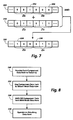
- Fig. 3 shows general acts in a method of operating a processor with processing circuitry like processing circuitry 90 in Fig. 2 to use a mask operand.
- the act in box 100 provides a composite operand and a mask operand to processing circuitry 90, with each component data item and its respective mask data item being provided to a respective subarray of processing positions 92.
- the act in box 102 operates processing circuitry 90 to perform a logic operation in parallel using the composite operand and mask operand to obtain a resulting data item in each subarray.
- Fig. 4 similarly shows general acts in a method of operating a processor with processing circuitry like processing circuitry 90 in Fig. 2 to obtain a mask operand.
- the act in box 106 provides a composite operand to processing circuitry 90, with each component being provided to a respective subarray of processing positions 92.
- the act in box 108 operates processing circuitry 90 to perform an operation on the composite operand to obtain a mask data item in each subarray.
- the mask data items together can form a mask operand.
- Fig 5 illustrates processor 110 with special circuitry that could be used to obtain mask data items in the act in box 108 of Fig. 4
- Processor 66 in Fig. 2 could be implemented using the features of processor 110.
- Processor 110 includes processing circuitry 120 with M processing positions 122 through 124.
- Processing circuitry 120 also includes K-bit shifting circuitry 126 for shifting bits K positions in a single cycle, where M>K.
- Control circuitry 128 provides control signals to processing circuitry 120 and specifically to K-bit shifting circuitry 126.
- the control signals can cause processing circuitry 120 to operate on a composite operand to obtain a resulting data item and a flag bit for each component.
- Each flag bit is positioned in a processing position adjacent the most significant bit of the component's subarray of processing positions 122 through 124.
- the control signals can also cause processing circuitry 120 and K-bit shifting circuitry 126 to perform an operation using the resulting data item and flag bit to obtain a flag bit operand in which the flag bit is in the least significant bit of the subarray and the other bits in the subarray all have either the same value as the flag bit or the same value as its inverse.
- the K-bit shifting circuitry 126 is therefore an optional performance enhancement that allows rapid shifting of the flag bit from adjacent the most significant bit to the least significant bit; if the distance between the two positions is not K bits, additional single shifts can be done before or after the K-bit shift.
- control signals can cause processing circuitry 120 to perform an arithmetic operation in parallel that uses the flag bit operand to obtain the mask operand.
- Figs. 6 and 7 illustrate implementations of the general steps shown in Fig. 4 that are applicable for processing units that can operate in parallel on more than one data item.
- Figs. 8-14 illustrate implementations of the general steps shown in Fig. 3 that are similarly applicable for processing units that can operate in parallel on more than one data item.
- the illustrated implementations could employ a number of such processing units operating in parallel with or without position connecting circuitry between them.
- Figs. 6 and 7 illustrate two implementations of the general acts described in relation to Fig. 4 that obtain mask operands from component data items in image processing.
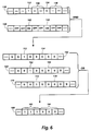
- Fig. 6 shows how a mask operand can be obtained by shifting and ORing an operand of flag bits.
- Fig. 7 shows how a mask operand can be obtained by an arithmetic operation on an operand of flag bits in the least significant bit positions.
- Operand 130 in Fig. 6 results from an operation that produced flag bits 132 and 134, each adjacent a most significant bit position of a component.
- Flag bit 132 indicates that a component in subarray 136 is in a first subset of components and flag bit 134 indicates that a component in subarray 138 is in a second subset.
- Operand 130 is ANDed with flag select operand 140.
- Flag select operand 140 has ON values in flag bit positions 142 and 144 and OFF values in all positions not containing flag bits. Therefore flag bit operand 150 has flag bit values 152 and 154 and zeros in positions not containing flag bits.
- Shifted flag bit operands 160 and 170 result from rightward shifts of flag bit operand 150, with flag bit values 162 and 164 shifted one bit rightward and flag bit values 172 and 174 shifted two bits rightward. Therefore, an OR operation on operands 150, 160, and 170 obtains mask operand 180.
- Mask data item 182 includes a uniform value of one in the bit positions of flag bit 132 and component 136.
- Mask data item 184 includes a uniform value of zero in the bit positions of flag bit 134 and component 138.
- the OR operation in Fig. 6 could be performed in stages, ORing the previous result with the shifted flag bit operand resulting from each shift operation to produce the next result.
- Fig. 6 can be modified to use an AND operation. Bits other than flag bits can start with the value one in the flag bit operand to make this possible.
- the technique of Fig. 6 can start with a flag bit at or adjacent either end of a component. If each component had an adjacent buffer bit, the flag bit can begin in the buffer bit to obtain a mask data item that also includes the buffer bit. If the flag bit is in the least significant bit of the component, however, the technique of Fig. 7 may be more efficient.
- Flag bit operand 200 includes flag bits 202 and 204.
- Flag bit 202 is the least significant bit of component 206, while flag bit 204 is the least significant bit of component 208.
- Flag bit operand 200 could be obtained in various ways. If components are divided into odd and even, flag bit operand 200 could be obtained simply by ANDing with an operand similar to operand 140 in Fig. 6 to select the flag bits. If the flag bit is initially positioned elsewhere, it can be selected and shifted, in either order, to obtain flag bit operand 200. If the flag bit begins at or adjacent the most significant bit of a component, K-bit shifting circuitry as shown in Fig. 5 can be used to move it more rapidly to the least significant bit.
- Flag bit operand 200 is added to constant operand 210, in which each data item has a value with a zero in its most significant bit and ones in all other bits.
- Constant data item 212 is added to data item 206 and constant data item 214 to data item 208.
- Flag bit operand 200 could instead be subtracted from a constant operand in which each data item has a value with a one in its most significant bit and zeros in all other bits. If flag bit operand 200 has a zero in the most significant bit position of each subarray, no borrow signals would propagate between subarrays.
- Mask operand 220 includes mask data items 222 and 224, with flag bit values 226 and 228 in their most significant bits, and with the opposite value in all other bits.
- Mask operand 220 can be used directly if the most significant bits are buffer bits that will be unaffected in use. Or the most significant bits could all be given a uniform value by an AND or OR operation. Or an XOR operation could be performed, either to invert all most significant bits or to invert all other bits.
- the technique of Fig. 7 may be more efficient than that of Fig. 6 if flag bit operand 200 can be efficiently obtained. Only one arithmetic operation is necessary to obtain mask operand 220.
- Figs. 8-14 illustrate implementations of the general acts described in relation to Fig. 3 that use mask operands to perform image processing operations.
- Fig. 8 shows how a mask operand can be used to select component data items on which an operation is performed.
- Fig. 9 shows how two results can be obtained using a mask operand and its inverse.
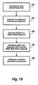
- Fig. 10 shows how mask operands can be used to obtain a maximum or minimum component at each position.
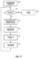
- Fig. 11 shows multiplication using mask operands.
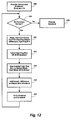
- Figs. 12 and 13 show division using mask operands.
- Fig. 14 shows threshold convolution using mask operands.
- the act in box 240 provides each component data item to a respective subarray of processing positions.
- this act can be an input operation that directly loads the components or it can be a series of image processing operations that uses input data to obtain the components in the subarrays.
- the act in box 242 uses each component data item to obtain a mask data item.
- this act is performed by obtaining one bit, such as a flag bit, that indicates whether the component is in a first subset or second subset.
- a flag bit such as a bit that indicates whether the component is in a first subset or second subset.
- the flag bit could indicate whether a component is equal to a constant, is greater than a threshold, or is within a range of values.
- the flag bit can then be used to obtain the mask data item, as discussed above in relation to Figs. 6 and 7.
- Each mask data item is uniformly OFF or uniformly ON in all its bits.
- the act in box 244 ANDs or ORs each component with its mask data item, as illustrated by the AND operation in Fig. 1. If ANDing, this act obtains the same value as the component if the mask data item is ON, but produces a value with zero in every bit if the mask data item is OFF. IF ORing, this act obtains the same value as the component if the mask data item is OFF, but produces a value with one in every bit if the mask data item is ON.
- composite operand 250 has been obtained by adding the value 10 to each component in composite operand 10 in Fig. 1. Carry signals between components have been prevented, such as with the techniques described in EP-A-0602888.
- Component 252 has the value 01, component 254 the value 00, and component 256 the value 11.
- Mask operand 260 is the inverse of mask operand 20 in Fig. 1, so that mask data items 262, 264, and 266 are inverted from mask data items 22, 24, and 26. As a result, mask operands 260 and 20 are complementary.
- Composite operand 250 and mask operand 260 are ANDed to obtain result 270, with resulting data items 272, 274, and 276.
- Data item 272 has the value 01 and data item 276 has the value 11 because mask data items 262 and 266 are ON.
- Result 270 is ORed with result 30 from Fig. 1 to obtain merged result 280.
- Data item 282 has the value of data item 272, data item 284 the value of data item 34, and data item 286 the value of data item 276. Therefore, merged result 280 is a version of composite operand 10 in which the value 10 has been added to components not equal to the value 10.
- Fig. 9 thus illustrates how mask operands can be used to select component data items on which an operation is performed.
- Fig. 9 also illustrates how a mask operand and its inverse can be used to obtain two results that can be merged.
- Fig. 10 illustrates another example of this use.
- the act in box 290 provides first and second composite operands, with each subarray receiving a pair of components, one from each composite operand.
- the act in box 292 then subtracts each first component from each second component, preventing borrow signals between components such as with the techniques described in EP-A-0602888. This subtraction produces sign flag bits as described in EP-A-0602887.
- the act in box 294 uses the sign flag bits to obtain a mask operand.
- the mask operand is ON in subarrays where the first operand is greater than the second operand and OFF elsewhere.
- the act in box 296 ANDs the mask operand with one of the two composite operands to produce one result and ANDs the inverted mask operand with the other composite operand to produce another result. If the mask is ANDed with the first operand and the inverted mask with the second operand, each result contains maximums. If the mask is ANDed with the second operand and the inverted mask with the first operand, each result contains minimums.
- the act in box 298 ORs the results from box 296 to obtain a merged result.
- the merged result includes the maximum value in all subarrays or the minimum value in all subarrays, depending on how the act in box 296 was performed.
- Fig. 10 could be modified by ORing in box 296 and ANDing in box 298. This will produce the same result if the composite operands were switched in box 296.
- Fig. 11 illustrates how mask operands can be used to perform multiplication.
- the act in box 300 provides two composite operands, a multiplier and a multiplicand, each with a plurality of multi-bit component data items.
- the act in box 300 obtains a product vector with a zero in each bit position.
- the act in box 310 begins a loop that iterates to handle each bit of the multiplier components. In other words, if every multiplier component has K bits, K iterations are performed.
- the act in box 312 obtains a mask operand using the value in the current bit position of each multiplier component as a flag bit.
- the current bit position can be either the most significant or the least significant bit.
- the act in box 312 can obtain a mask as described above in relation to Figs. 6 and 7.
- the act in box 316 adds the resulting data item from box 314 to the product vector. Then, the act in box 318 shifts the product vector and multiplier by one bit to prepare for the next iteration. If the current position is the most significant bit, the shift can be leftward; if the least significant, rightward.
- the act in box 320 provides the product.
- This act can include any shifting necessary to position the product data items appropriately, such as a K-bit shift to the left after K rightward shifts in box 318.
- the acts in boxes 316 and 318 together can produce a product that extends beyond K bits. For example, if the values of both a multiplier component and the aligned multiplicand component are equal to (2 K - 1), the product is (2 2K - 2 (K+1) + 1), which requires 2 K bits for K > 2. Therefore, the acts in Fig. 9 must be performed in a way that prevents inter-component signals from causing invalid results.
- the act in box 300 can perform a spreading operation. If leftward shifting is performed in box 318, the spreading operation can add K zero bits adjacent the most significant bit of each component, but if rightward shifting is performed, the spreading operation can add K zero bits adjacent the least significant bit.
- Another way to ensure valid results is to include a buffer bit adjacent each component data item in the multiplier, multiplicand, and product. This approach permits operations on more components in parallel, but produces single precision multiplication results, since each product data item includes only K bits.
- the buffer bits could be inserted by the act in box 300 and could be cleared in the multiplier and product before or after each iteration of the loop beginning with box 310.
- the act in box 312 could obtain a mask data item from the most significant bit, and the act in box 318 could shift leftward
- the act in box 300 could preshift the multiplier rightward by (K-1) bits to position the most significant bit in the least significant bit's position, allowing use of the technique shown in Fig. 7, above.
- the act in box 312 could obtain a mask data item from the least significant bit, and the act in box 318 could shift rightward.
- Fig. 12 illustrates how mask operands can be used to perform division.
- the act in box 340 provides two composite operands, a divisor and a dividend, each with plural multi-bit component data items.
- the divisor and dividend both have a buffer bit adjacent the most significant bit of each component, and the buffer bits begin with the value zero.
- the act in box 340 obtains a quotient vector with a zero in each bit position.
- the act in box 350 begins a loop that iterates to handle each bit of the dividend. Each iteration handles the bit that is currently the most significant bit of the dividend.
- the act in box 352 begins by subtracting the divisor from the dividend after setting all dividend buffer bits to the value one. If a divisor component is greater than a dividend component, the subtraction produces a difference and a borrow signal that changes the adjacent buffer bit to the value zero, providing a sign flag bit.
- the act in box 354 ANDs the result from box 352 with a buffer bit select operand that is ON in each buffer bit position and OFF elsewhere, to obtain a flag bit operand.
- the act in box 354 also ORs the flag bit operand with the quotient to update the quotient.
- the act in box 356 inverts the flag bit operand and uses the inverted flag bits to obtain a mask operand using techniques like those described above in relation to Figs. 6 and 7, but with OFF in every buffer bit position.
- the act in box 356 then ANDs the mask operand with the divisor to select each divisor component that led to a negative difference data item.
- box 358 adds the selected divisors from box 356 to the difference from box 352 to obtain the next dividend.
- the buffer bits in the difference can be given the value zero by an AND operation. Wherever the difference was negative, the divisor is therefore added back in to restore a positive value.
- the act in box 360 then shifts the next dividend and the quotient.
- the act in box 360 also does an AND operation to give all buffer bits in the shifted next dividend the value zero.
- the act in box 370 provides the quotient.
- the quotient can be shifted as appropriate before it is provided, such as K rightward shifts after K leftward shifts in box 360.
- Fig. 12 can be modified for special situations. For example, if divisor components always have values much smaller than dividend components, more meaningful quotient data items may be obtained by beginning with the divisor shifted leftward an appropriate number of bits. In general, the shifted divisor should have a value at least half that of the dividend.
- Non-restoring division could be performed by modifying a conventional non-restoring dividend algorithm:
- a mask operand could be created.
- the mask and its inverse could be used to select either the positive or negative version of the divisor component in each subarray.
- the quotient could be obtained by adding a vector of buffer bits if a previous result is positive and subtracting a vector of inverted buffer bits if the previous result is negative, again using a mask and its inverse.
- division can obtain resulting data items of a different length than the dividend and divisor components. If all dividends have K-bit components and all divisors have (K/2)-bit components, (K/2)-bit quotients can be obtained. Then the result can be subsampled or reduced to eliminate unnecessary bit positions.
- Fig. 13 shows acts that can perform division of arbitrary K-bit values.
- the act in box 400 provides a divisor and dividend and initializes a quotient as box 340 in Fig. 10.
- the act in box 400 also initializes an index i to zero.
- the act in box 410 begins the first of three loops.
- the first loop iterates to obtain a first mask operand for each value of i .
- the second loop iterates to obtain a second mask operand for each value of i using the first mask operands.
- the third loop uses the second mask operands to select subarrays in which to obtain a quotient bit.
- the act in box 412 in the first loop obtains mask M i using the least significant bit of each divisor component as a flag bit.
- a technique for rapidly obtaining a mask from least significant bits of components is described above in relation to Fig. 7.
- the act in box 414 finishes the first loop by shifting the divisor rightward and by incrementing i .
- the first loop produces K masks M o through M (K-1) .
- the act in box 416 prepares for the second loop.
- Mask M (K-1) is treated as modified mask MA (K-1) , one of K modified masks.
- the index i starts again at 0.
- the act in box 420 begins (K-1) iterations of the second loop.
- the second loop is performed by the act in box 422.
- Modified mask MA (K-2-i) is obtained by ORing masks MA (K-1-i) and M (K-2-i) . Index i is incremented.
- the second loop thus produces K masks MA o through MA (K-1) . For every divisor component, if the most significant bit is in bit i , then masks MA i+1 through MA (K-1) are all zeros and masks MA o through MA i are all ones.
- the act in box 424 prepares for division by shifting each mask MA i leftward i bits, aligning it so that shifted divisor components do not affect each other.
- the act in box 424 also shifts the divisor left K bits to its original position, and returns i to zero.
- the act in box 430 begins K iterations of the third loop. Each iteration obtains one quotient bit for each component, either through restoring or non-restoring division.
- the act in box 432 in the third loop ANDs the current divisor components with mask MA i to select divisor components.
- the act in box 434 uses the selected divisor components and the dividend to obtain the next quotient bit, and updates the dividend.
- the act in box 436 ANDs the quotient with mask MA i to zero any quotient bits in non-selected subarrays. This act ensures that no operation is performed on a divisor component until its most significant non-zero bit is aligned with the most significant bit of the dividend.
- the act in box 438 then prepares for the next iteration by shifting the divisor rightward, shifting the quotient leftward, and incrementing i .
- the act in box 438 can clear the buffer bits in the divisor.
- the act in box 440 provides the quotient, shifted if appropriate.
- Fig. 13 illustrates that complex, conditional tasks can be implemented using mask operands to perform conditional branches.
- Fig. 14 illustrates threshold convolution.
- Threshold convolution receives one-bit data items and produces one-bit data items, but uses multi-bit data items in intermediate operations.
- a structure element is a matrix of integer weights with a position defined in relation to a destination position. The structure element is positioned in the source bitmap and the integer weights in the same positions as ones in the bitmap are summed. The sum is compared to a threshold. If the threshold is exceeded, the destination position is one, otherwise zero.
- the source and destination data items are illustratively pixel values, but the illustrated implementation could be applied to other arrays of data items.
- the act in box 460 spreads source pixels to obtain masks that include mask data items with as many bits as each integer weight in the structure element.
- the act in box 462 uses the masks from box 460 to select weights on source pixels that have the value one. The selected weights are added to obtain a sum for each position of the structure element.
- the act in box 464 compares the sums with a threshold to obtain sign flag bits indicating values of destination pixels.
- the act in box 466 subsamples the result from box 464 to select only the destination pixels.
- the technique of Fig. 14 maintains a sum for every structure element position.
- the technique also requires extensive shifting to position masks in relation to weights. It might be possible to reduce these inefficiencies by providing sums when completed, by reclaiming memory occupied by a completed sum after it is provided, and by finding ways to perform fewer shift operations.
- Threshold convolution could also be performed without masking. For example, a sequence of source bits could be used to access a lookup table to obtain sums for a few destination positions, and the sums could be obtained and used to produce destination bits.
- serial operation involves some branching, but not extensive branching, it can be converted to a reasonably effective parallel operation.
- the parallel operation could, for example be implemented on a SIMD machine.
- One guideline for converting from serial to parallel operations relates to binary branching. If a branch would cause an ideal processor to perform either suboperation A or suboperation B depending on data item value, obtain a flag bit for each component data item indicating whether suboperation A or B should be performed on it. Use the flag bits to obtain a mask operand. Perform both suboperations A and B on all components in parallel. AND the A results with the mask operand, AND the B results with the inverse of the mask operand; and OR the ANDed results to obtain a merged result.
- Another guideline relates to operations that are iterated as many times as indicated by a data item. Perform an operation as many times as necessary for the worst case, but use masks to control the calculation for each component, as illustrated in Fig. 13.
- Masks can be used, for example, to prevent results from being saved until a certain number of iterations remain. Or masks can be used to prevent results from being updated after a certain number of iterations.
- the general implementation features described above could be used in a wide variety of data processing applications. They are expected to be particularly useful, however, in performing some types of image processing more rapidly than they could be performed serially on each data item.
- the features described above could be used to implement techniques similar to those described in Serra, J., Image Analysis and Mathematical Morphology , Academic Press, 1982 and Serra, J., Image Analysis and Mathematical Morphology , Volume 2: Theoretical Advances, Academic Press, 1988 .
- Such techniques may be used, for example, to provide document services, such as removal of noise or other non-informative features, skew correction, data encoding, extraction of segments for automatic form or control sheet creation, and printer specific correction.
- Such document services can be used in digital copying machines, including fax machines and photocopying machines, in machines that produce data defining an image for a printer or other image output device, in machines that operate on data defining an image received from a scanner or other image input device, and in other machines that perform image processing.
- the general implementation features described above may also be useful in various other applications, such as searching an image database for images containing a particular set of features; scanning envelopes for addresses; interpreting forms from a high-speed scanner; machine vision; and process-specific print image correction and verification.
- the invention could also be applied to perform various other image processing operations, such as pixel counting, gray scale morphology, gray scale rotation, generating error-diffused images, and skew detection.
- the invention could also be used with data that do not relate to an image.
- the invention could be used, for example, to perform finite difference analysis or simulations of physical phenomena.
- the invention has been described in relation to implementations in which a mask operand has ON bits aligned with component data items to be selected and OFF bits elsewhere, and an AND operation is performed on the mask operand and a composite operand to select components.
- the invention could also be implemented with a mask operand that has OFF bits aligned with components to be selected and ON bits elsewhere, by performing an OR operation on the mask operand and a composite operand to select components.
- the invention has been described in relation to implementations in which a flag bit is obtained adjacent a component data item.
- the invention could also be implemented with a flag bit obtained at any other position from which it can be propagated across a component, such as a position within the component.
- the invention has been described in relation to implementations in which flag bits are used directly to obtain a mask operand.
- the invention might also be implemented in ways that invert flag bits or otherwise modify them before using them to obtain a mask operand. For example, all flag bits could be inverted with an XOR operation without affecting other bits.
- the invention has been described in relation to implementations in which flag bits are used to obtain a mask operand by shifting and ORing a flag bit operand or by performing an arithmetic operation in parallel on the flag bit operand and a constant operand.
- the invention might also be implemented with other techniques for using flag bits to obtain a mask operand.
- the invention has been described in relation to implementations that operate on data relating to images, but might also be implemented to operate on data that do not relate to an image.
- the invention has been described in relation to implementations with conventional microprocessors, but the invention might also be implemented with reduced instruction set (RISC) chips or with any other processor, including the processor of a mainframe computer, minicomputer, supercomputer, or any other computing device.
- RISC reduced instruction set
- the invention has been described in relation to a software product for use in a system that includes a processor and memory, with the software product storing data indicating instructions the processor can execute to perform operations on data from memory.
- the system's memory can, of course, include the software product when in use in the system, and instructions and data can, in general, be arbitrarily stored in any memory device accessible by the processor; for example, the invention can readily be implemented with data indicating instructions stored in memory rather than in a software product.
- the invention has been described in relation to composite operands with simple structures.
- all component data items are of the same length and the components within a composite operand need not be related to each other.
- the invention could also be implemented with composite operands with additional structure, within the limitations of processor width.
- a composite operand could include component data items of different widths, provided that other operands are aligned with components of the same widths in the same positions.
- the component data items could be arranged in groups of two or more, with the components in each group being related: If the components in each group relate to the same pixel, each component could hold a value for a respective threshold reduction. More generally, if the components in each group relate to the same location in a physical simulation space, one component could hold a value for the location and the other locations could hold derivatives at the location.
Landscapes
- Engineering & Computer Science (AREA)
- Theoretical Computer Science (AREA)
- Physics & Mathematics (AREA)
- Software Systems (AREA)
- General Engineering & Computer Science (AREA)
- General Physics & Mathematics (AREA)
- Mathematical Physics (AREA)
- Executing Machine-Instructions (AREA)
- Advance Control (AREA)
Claims (13)
- Procédé de mise en oeuvre d'un processeur (66 ; 110), le procédé comprenant les étapes consistant à :A) mettre en oeuvre le processeur en utilisant un opérande composite (10 ; 250) et un opérande de masque (20 ; 180 ; 220 ; 260), l'opérande composite comprenant deux ou plusieurs éléments de données de composants (12, 14, 16 ; 252, 254, 256), chacun comprenant plus d'un bit, l'opérande de masque comprenant, pour chaque bit de l'opérande composite, un bit de masque respectif, les éléments de données de composants comprenant un premier sous-ensemble et un second sous-ensemble, le bit de masque de chaque bit du premier sous-ensemble présentant une première valeur, le bit de masque de chaque bit du second sous-ensemble présentant une seconde valeur,
caractérisé en ce que l'opérande composite et l'opérande de masque sont alignés dans le processeur, chaque bit de l'opérande composite étant aligné avec son bit de masque, et en ce que A) comprend au moins un élément suivant :A1) mettre en oeuvre le processeur pour utiliser l'opérande composite afin d'obtenir l'opérande de masque (180 ; 220), etA2) mettre en oeuvre le processeur pour exécuter une opération logique en parallèle en utilisant l'opérande composite (10 ; 250) et l'opérande de masque (20 ; 260) afin d'obtenir un résultat (30 ; 270). - Procédé selon la revendication 1 dans lequel le processeur (66 ; 110) comporte un tableau de positions de traitement (92 ; 122, 124), chacune destinée à exécuter des opérations sur un bit, les positions de traitement exécutant des opérations en parallèle, chaque élément de données de composant de l'opérande composite se trouvant dans un sous-tableau respectif des positions de traitement, chaque bit de l'opérande composite (10 ; 250) et son bit de masque étant aligné avec une position de traitement respective.
- Procédé selon la revendication 2 dans lequel A1) comprend :A1a) mettre en oeuvre le processeur (66 ; 110) pour obtenir, dans le sous-tableau de chaque élément de données de composant, un élément de données de masque respectif.
- Procédé selon la revendication 3 dans lequel le sous-tableau de chaque élément de données de composant comprend une extrémité du sous-tableau, le tableau de positions de traitement (92 ; 122, 124) comprenant, à l'extrémité de chaque sous-tableau, une position de bit d'indicateur respectif, A1a) comprenant :une opération de bit d'indicateur qui utilise l'opérande composite pour obtenir un opérande de bit d'indicateur (150), l'opérande de bit d'indicateur comprenant la première valeur à la position de bit d'indicateur de chaque élément de données de composant dans le premier sous-ensemble et la seconde valeur à la position de bit d'indicateur de chaque élément de données de composant dans le second sous-ensemble, l'opérande de bit d'indicateur comprenant en outre la seconde valeur dans toutes les autres positions de traitement du sous-tableau de chaque élément de données de composant,une série de sous-opérations, chaque sous-opération permettant d'obtenir une version décalée respective de l'opérande de bit d'indicateur, etune opération logique qui utilise l'opérande de bit d'indicateur et les versions décalées de l'opérande de bit d'indicateur pour obtenir l'opérande de masque (180).
- Procédé selon la revendication 3 dans lequel le sous-tableau de chaque élément de données de composant comprend au moins un bit significatif à une extrémité du sous-tableau, A1a) comprenant :une opération de bit d'indicateur qui utilise l'opérande composite pour obtenir un opérande de bit d'indicateur (200), l'opérande de bit d'indicateur comprenant la première valeur à la position du bit le moins significatif de chaque élément de données de composant dans le premier sous-ensemble et la seconde valeur à la position du bit le moins significatif de chaque élément de données de composant dans le second sous-ensemble, l'opérande de bit d'indicateur comprenant en outre la seconde valeur à toutes les autres positions de traitement du sous-ensemble de chaque élément de données de composant, etune opération arithmétique en parallèle qui utilise l'opérande de bit d'indicateur pour obtenir l'opérande de masque (220).
- Procédé selon la revendication 5 dans lequel le sous-tableau de chaque élément de données de composant comprend une position de bit le plus significatif à une première extrémité du sous-tableau et la position de bit le moins significatif à une seconde extrémité du sous-tableau, chaque sous-tableau comprenant en outre une position de bit d'indicateur à proximité de la première extrémité du sous-tableau, le processeur comprenant en outre un circuit de décalage à K bits (126) pour décaler un opérande de K bits dans les positions de traitement (122, 124), où K est supérieur à un, l'opération de bit d'indicateur comprenant :l'utilisation de chaque élément de données de composant pour obtenir un élément de données résultant respectif dans le sous-tableau de l'élément de données de composant et un bit d'indicateur respectif à la position de bit d'indicateur du sous-tableau, le bit d'indicateur présentant la première valeur si l'élément de données de composant est dans le premier sous-ensemble et présentant la seconde valeur si l'élément de données de composant est dans le second sous-ensemble, etune opération de décalage/sélection d'indicateur utilisant les éléments de données résultants et les bits indicateurs des éléments de données de composants pour obtenir l'opérande de bit d'indicateur, l'opération de décalage/sélection d'indicateur comprenant une opération de circuit de décalage à K bits pour décaler le bit d'indicateur de chaque élément de données de composant de K bits en décalant le bit d'indicateur depuis la position de bit d'indicateur jusqu'à la position de bit le moins significatif,l'opération arithmétique obtenant, dans le sous-tableau de chaque élément de données de composant, un élément de données de masque respectif, l'élément de données de masque comprenant, pour chaque bit de l'élément de données de composant, un bit respectif aligné avec le bit de l'élément de données de composant, chaque bit d'un élément de données de masque aligné avec un bit d'un élément de données de composant du premier sous-ensemble présentant la première valeur, chaque bit d'un élément de données de masque aligné avec un bit d'un élément de données de composant dans le second sous-ensemble présentant la seconde valeur, les éléments de données de masque formant ensemble l'opérande de masque (220).
- Procédé selon la revendication 2 dans lequel A2) comprend :la fourniture de l'opérande composite (10 ; 250) et de l'opérande de masque (20 ; 260) au tableau de positions de traitement (92 ; 122, 124), l'opérande de masque comprenant, pour chaque élément de données de composant de l'opérande composite, un élément de données de masque respectif qui est fourni au sous-tableau de positions de traitement de l'élément de données de composant, etl'exploitation du tableau de positions de traitement pour exécuter l'opération logique en vue d'obtenir, dans le sous-tableau de chaque élément de données de composant, un élément de données résultant respectif, l'élément de données résultant de chaque élément de données de composant du premier sous-ensemble présentant la même valeur que l'élément de données de composant, l'élément de données résultant de chaque élément de données de composant du second sous-ensemble présentant une valeur uniforme pour tous les bits, la valeur uniforme pour les bits de l'élément de données résultant de chaque élément de données de composant dans le second sous-ensemble étant l'une de la première valeur et de la seconde valeur.
- Procédé selon la revendication 7 dans lequel la première valeur est ACTIF, la seconde valeur est INACTIF, l'opération logique est une opération ET, et la valeur uniforme est la seconde valeur.
- Procédé selon la revendication 7 ou la revendication 8, comprenant en outre :B) mettre en oeuvre le processeur (66 ; 110) pour exécuter une opération supplémentaire en parallèle en utilisant les éléments de données résultants, l'opération supplémentaire permettant d'obtenir, dans le sous-tableau de chaque élément de données de composant dans le premier sous-ensemble, un élément de données résultant modifié respectif, l'opération supplémentaire permettant d'obtenir, dans le sous-tableau de chaque élément de données de composant du second sous-ensemble, un élément de données résultant non modifié respectif, les éléments de données résultants modifiés et les éléments de données résultants non modifiés formant ensemble un opérande résultant modifié.
- Procédé selon la revendication 9 dans lequel B) comprend :mettre en oeuvre le processeur (66 ; 110) pour exécuter une seconde opération logique en parallèle utilisant l'opérande de masque (20 ; 260), l'opérande composite (10 ; 250), et l'opérande résultant modifié pour obtenir une version modifiée de l'opérande composite, la version modifiée de l'opérande composite comprenant les éléments de données résultants modifiés.
- Procédé selon la revendication 7 ou la revendication 8, comprenant en outre :C) la fourniture au processeur (66 ; 110) d'un second opérande composite (250) et d'un second opérande de masque (260), le second opérande composite comprenant deux éléments de données de composants ou plus, chacun comprenant plus d'un bit et chacun étant procuré à un sous-tableau respectif des positions de traitement (92 ; 122, 124), le sous-tableau de chaque élément de données de composant du second opérande composite étant aligné avec le sous-tableau d'un élément de données de composant respectif du premier opérande composite (10), le second opérande de masque comprenant, pour chaque élément de données de composant, un élément de données de masque respectif qui est procuré au sous-tableau de positions de traitement de l'élément de données de composant, chaque élément de données de masque comprenant, pour chaque bit de l'élément de données de composant, un bit de masque respectif aligné avec le bit de l'élément de données de composant, les éléments de données de composants du second opérande composite comprenant un premier sous-ensemble et un second sous-ensemble, le sous-tableau de chaque élément de données de composant du premier sous-ensemble étant aligné avec le sous-tableau d'un élément respectif du premier sous-ensemble des éléments de données de composants du premier opérande composite et le sous-tableau de chaque élément de données de composant du second sous-ensemble étant aligné avec le sous-tableau d'un élément respectif du second sous-ensemble des éléments de données de composants dans le premier opérande composite de sorte que chaque bit dans chaque élément de données de masque du second opérande de masque est aligné avec un bit respectif d'un élément de données de masque du premier opérande de masque (20), chaque bit de chaque élément de données de masque du second opérande de masque étant un inverse du bit respectif de l'élément de données de masque respectif du premier opérande de masque, le bit de l'élément de données de masque du second opérande de masque présentant la première valeur si le bit respectif de l'élément de données de masque du premier opérande de masque présente la seconde valeur et présentant la seconde valeur si le bit respectif de l'élément de données de masque du premier opérande de masque présente la première valeur,D) mettre en oeuvre le processeur pour exécuter une seconde opération logique en parallèle utilisant le second opérande composite et le second opérande de masque, la seconde opération logique permettant d'obtenir, dans le sous-tableau de chaque élément de données de composant du second opérande composite, un élément de données résultant respectif, chaque élément de données résultant d'un élément de données de composant du second sous-ensemble présentant la même valeur que l'élément de données de composant, chaque élément de données résultant d'un élément de données de composant du premier sous-ensemble présentant la valeur uniforme pour tous les bits, etE) mettre en oeuvre le processeur pour exécuter une troisième opération logique en parallèle utilisant les éléments de données résultants des éléments de données de composants des premier et second opérandes composites, la troisième opération logique permettant d'obtenir un résultat (280) qui comprend l'élément de données résultant de chaque élément de données de composant du premier opérande composite du premier sous-ensemble et l'élément de données résultant de chaque élément de données de composant du second opérande composite du second sous-ensemble.
- Procédé selon la revendication 11 dans lequel le résultat (280) comprend soit le maximum soit le minimum de chaque paire d'éléments de données de composants alignés des premier et second opérandes composites.
- Système comprenant :un moyen de mémorisation (62, 64) destiné à mémoriser des données d'instructions (80, 82),un processeur (66 ; 110) relié pour recevoir des données d'instructions depuis le moyen de mémorisation,
caractérisé en ce que les données d'instructions indiquent les instructions que le processeur peut exécuter pour réaliser des opérations utilisant un opérande composite (10 ; 250) et un opérande de masque (20 ; 180; 220 ; 260), l'opérande composite comprenant deux ou plusieurs éléments de données de composants (12, 14, 16 ; 252, 254; 256), chacun comprenant plus d'un bit, l'opérande de masque comprenant, pour chaque bit de l'opérande composite, un bit de masque respectif, les éléments de données de composants comprenant un premier sous-ensemble et un second sous-ensemble, le bit de masque de chaque bit du premier sous-ensemble présentant une première valeur, le bit de masque de chaque bit du second sous-ensemble présentant une seconde valeur, l'opérande composite et l'opérande de masque étant alignés dans le processeur, chaque bit de l'opérande composite étant aligné avec son bit de masque,
caractérisé en outre en ce que les instructions comprennent au moins l'un des éléments suivants :un masque obtenant des instructions (80) que le processeur peut exécuter pour utiliser l'opérande composite afin d'obtenir l'opérande de masque (180 ; 220), etun masque utilisant des instructions (82) que le processeur peut exécuter pour réaliser une opération logique en parallèle en utilisant l'opérande composite (10 ; 250) et l'opérande de masque (20 ; 260) afin d'obtenir un résultat (30 ; 270).
Applications Claiming Priority (2)
| Application Number | Priority Date | Filing Date | Title |
|---|---|---|---|
| US07/993,938 US5651121A (en) | 1992-12-18 | 1992-12-18 | Using mask operand obtained from composite operand to perform logic operation in parallel with composite operand |
| US993938 | 1992-12-18 |
Publications (3)
| Publication Number | Publication Date |
|---|---|
| EP0602886A2 EP0602886A2 (fr) | 1994-06-22 |
| EP0602886A3 EP0602886A3 (en) | 1994-09-07 |
| EP0602886B1 true EP0602886B1 (fr) | 2000-03-15 |
Family
ID=25540099
Family Applications (1)
| Application Number | Title | Priority Date | Filing Date |
|---|---|---|---|
| EP93309860A Expired - Lifetime EP0602886B1 (fr) | 1992-12-18 | 1993-12-08 | Masque pour la sélection de composants multibit d'un opérande composé |
Country Status (4)
| Country | Link |
|---|---|
| US (1) | US5651121A (fr) |
| EP (1) | EP0602886B1 (fr) |
| JP (1) | JP3584053B2 (fr) |
| DE (1) | DE69328070T2 (fr) |
Families Citing this family (42)
| Publication number | Priority date | Publication date | Assignee | Title |
|---|---|---|---|---|
| US5751614A (en) * | 1994-03-08 | 1998-05-12 | Exponential Technology, Inc. | Sign-extension merge/mask, rotate/shift, and boolean operations executed in a vectored mux on an ALU |
| US6385634B1 (en) * | 1995-08-31 | 2002-05-07 | Intel Corporation | Method for performing multiply-add operations on packed data |
| US7395298B2 (en) * | 1995-08-31 | 2008-07-01 | Intel Corporation | Method and apparatus for performing multiply-add operations on packed data |
| JPH0969047A (ja) * | 1995-09-01 | 1997-03-11 | Sony Corp | Risc型マイクロプロセッサおよび情報処理装置 |
| JP3433588B2 (ja) * | 1995-10-19 | 2003-08-04 | 株式会社デンソー | マスクデータ生成回路及びビットフィールド操作回路 |
| US5907842A (en) * | 1995-12-20 | 1999-05-25 | Intel Corporation | Method of sorting numbers to obtain maxima/minima values with ordering |
| US6036350A (en) * | 1995-12-20 | 2000-03-14 | Intel Corporation | Method of sorting signed numbers and solving absolute differences using packed instructions |
| US5983291A (en) * | 1996-09-24 | 1999-11-09 | Cirrus Logic, Inc. | System for storing each of streams of data bits corresponding from a separator thereby allowing an input port accommodating plurality of data frame sub-functions concurrently |
| US5832288A (en) * | 1996-10-18 | 1998-11-03 | Samsung Electronics Co., Ltd. | Element-select mechanism for a vector processor |
| US5946222A (en) * | 1996-12-20 | 1999-08-31 | Oak Technology, Inc. | Method and apparatus for performing a masked byte addition operation |
| US20030068623A1 (en) * | 1997-06-16 | 2003-04-10 | Genentech, Inc. | Secreted and transmembrane polypeptides and nucleic acids encoding the same |
| US6117508A (en) | 1997-06-27 | 2000-09-12 | Dyneon Llc | Composite articles including a fluoropolymer blend |
| US6081824A (en) * | 1998-03-05 | 2000-06-27 | Intel Corporation | Method and apparatus for fast unsigned integral division |
| JP4131349B2 (ja) * | 1998-12-09 | 2008-08-13 | ソニー株式会社 | データ変換装置およびデータ変換方法、記録媒体、並びにデータ変換システム |
| US6470440B1 (en) * | 1999-05-20 | 2002-10-22 | International Business Machines Corporation | Vector compare and maximum/minimum generation apparatus and method therefor |
| US7120781B1 (en) * | 2000-06-30 | 2006-10-10 | Intel Corporation | General purpose register file architecture for aligned simd |
| JPWO2002037260A1 (ja) * | 2000-10-24 | 2004-03-11 | 日新電機株式会社 | 乱数発生装置 |
| US6944753B2 (en) * | 2001-04-11 | 2005-09-13 | International Business Machines Corporation | Fixed point unit pipeline allowing partial instruction execution during the instruction dispatch cycle |
| US6985986B2 (en) * | 2001-06-01 | 2006-01-10 | Microchip Technology Incorporated | Variable cycle interrupt disabling |
| US20020184566A1 (en) | 2001-06-01 | 2002-12-05 | Michael Catherwood | Register pointer trap |
| US7467178B2 (en) | 2001-06-01 | 2008-12-16 | Microchip Technology Incorporated | Dual mode arithmetic saturation processing |
| US6975679B2 (en) | 2001-06-01 | 2005-12-13 | Microchip Technology Incorporated | Configuration fuses for setting PWM options |
| US7020788B2 (en) | 2001-06-01 | 2006-03-28 | Microchip Technology Incorporated | Reduced power option |
| US7003543B2 (en) * | 2001-06-01 | 2006-02-21 | Microchip Technology Incorporated | Sticky z bit |
| US7007172B2 (en) | 2001-06-01 | 2006-02-28 | Microchip Technology Incorporated | Modified Harvard architecture processor having data memory space mapped to program memory space with erroneous execution protection |
| US6952711B2 (en) | 2001-06-01 | 2005-10-04 | Microchip Technology Incorporated | Maximally negative signed fractional number multiplication |
| US6937084B2 (en) | 2001-06-01 | 2005-08-30 | Microchip Technology Incorporated | Processor with dual-deadtime pulse width modulation generator |
| US6976158B2 (en) | 2001-06-01 | 2005-12-13 | Microchip Technology Incorporated | Repeat instruction with interrupt |
| US6934728B2 (en) | 2001-06-01 | 2005-08-23 | Microchip Technology Incorporated | Euclidean distance instructions |
| US7430578B2 (en) * | 2001-10-29 | 2008-09-30 | Intel Corporation | Method and apparatus for performing multiply-add operations on packed byte data |
| US7430574B2 (en) * | 2004-06-24 | 2008-09-30 | Intel Corporation | Efficient execution and emulation of bit scan operations |
| US7610472B2 (en) * | 2005-06-05 | 2009-10-27 | Apple Inc. | Performing variable and/or bitwise shift operation for a shift instruction that does not provide a variable or bitwise shift option |
| WO2007083199A1 (fr) * | 2006-01-18 | 2007-07-26 | Freescale Semiconductor, Inc. | Dispositif et procédé de recherche de valeurs extrêmes dans un bloc de données |
| US9069547B2 (en) | 2006-09-22 | 2015-06-30 | Intel Corporation | Instruction and logic for processing text strings |
| US9003170B2 (en) * | 2009-12-22 | 2015-04-07 | Intel Corporation | Bit range isolation instructions, methods, and apparatus |
| US9323531B2 (en) * | 2013-03-15 | 2016-04-26 | Intel Corporation | Systems, apparatuses, and methods for determining a trailing least significant masking bit of a writemask register |
| US9880839B2 (en) * | 2014-04-24 | 2018-01-30 | Intel Corporation | Instruction that performs a scatter write |
| US9262704B1 (en) * | 2015-03-04 | 2016-02-16 | Xerox Corporation | Rendering images to lower bits per pixel formats using reduced numbers of registers |
| US10423411B2 (en) * | 2015-09-26 | 2019-09-24 | Intel Corporation | Data element comparison processors, methods, systems, and instructions |
| US11500680B2 (en) * | 2020-04-24 | 2022-11-15 | Alibaba Group Holding Limited | Systolic array-friendly data placement and control based on masked write |
| US11410580B2 (en) * | 2020-08-20 | 2022-08-09 | Facebook Technologies, Llc. | Display non-uniformity correction |
| CN112799637B (zh) * | 2021-01-22 | 2023-03-14 | 西安电子科技大学 | 一种并行环境下高吞吐量的模逆计算方法及系统 |
Family Cites Families (31)
| Publication number | Priority date | Publication date | Assignee | Title |
|---|---|---|---|---|
| US4139899A (en) * | 1976-10-18 | 1979-02-13 | Burroughs Corporation | Shift network having a mask generator and a rotator |
| US4180861A (en) * | 1978-03-31 | 1979-12-25 | Ncr Corporation | Selectively operable mask generator |
| DE3040931C1 (de) * | 1980-10-30 | 1982-04-29 | Siemens AG, 1000 Berlin und 8000 München | Verfahren und Anordnung zur Verknuepfung von Operanden variabler Laenge in Datenverarbeitungsanlagen |
| US4592005A (en) * | 1982-07-06 | 1986-05-27 | Sperry Corporation | Masked arithmetic logic unit |
| US4785393A (en) * | 1984-07-09 | 1988-11-15 | Advanced Micro Devices, Inc. | 32-Bit extended function arithmetic-logic unit on a single chip |
| US5034900A (en) * | 1984-10-05 | 1991-07-23 | Hitachi, Ltd. | Method and apparatus for bit operational process |
| JPS6266377A (ja) * | 1985-09-19 | 1987-03-25 | Fujitsu Ltd | マスクパタ−ン生成方式 |
| US5056041A (en) * | 1986-12-31 | 1991-10-08 | Texas Instruments Incorporated | Data processing apparatus with improved bit masking capability |
| US4775952A (en) * | 1986-05-29 | 1988-10-04 | General Electric Company | Parallel processing system apparatus |
| US5060280A (en) * | 1986-09-30 | 1991-10-22 | Canon Kabushiki Kaisha | Masking control for image processing systems |
| US4864529A (en) * | 1986-10-09 | 1989-09-05 | North American Philips Corporation | Fast multiplier architecture |
| US5129092A (en) * | 1987-06-01 | 1992-07-07 | Applied Intelligent Systems,Inc. | Linear chain of parallel processors and method of using same |
| JP2613223B2 (ja) * | 1987-09-10 | 1997-05-21 | 株式会社日立製作所 | 演算装置 |
| US5129066A (en) * | 1987-09-17 | 1992-07-07 | International Business Machines Corporation | Bit mask generator circuit using multiple logic units for generating a bit mask sequence |
| US4953119A (en) * | 1989-01-27 | 1990-08-28 | Hughes Aircraft Company | Multiplier circuit with selectively interconnected pipelined multipliers for selectively multiplication of fixed and floating point numbers |
| US5065437A (en) * | 1989-12-08 | 1991-11-12 | Xerox Corporation | Identification and segmentation of finely textured and solid regions of binary images |
| US5131049A (en) * | 1989-12-08 | 1992-07-14 | Xerox Corporation | Identification, characterization, and segmentation of halftone or stippled regions of binary images by growing a seed to a clipping mask |
| US5048109A (en) * | 1989-12-08 | 1991-09-10 | Xerox Corporation | Detection of highlighted regions |
| US5267051A (en) * | 1989-12-22 | 1993-11-30 | Eastman Kodak Company | High speed compression of imagery data |
| US5214763A (en) * | 1990-05-10 | 1993-05-25 | International Business Machines Corporation | Digital computer system capable of processing two or more instructions in parallel and having a coche and instruction compounding mechanism |
| US5280547A (en) * | 1990-06-08 | 1994-01-18 | Xerox Corporation | Dense aggregative hierarhical techniques for data analysis |
| JPH0454679A (ja) * | 1990-06-25 | 1992-02-21 | Nec Corp | 演算装置 |
| JP2601960B2 (ja) * | 1990-11-15 | 1997-04-23 | インターナショナル・ビジネス・マシーンズ・コーポレイション | データ処理方法及びその装置 |
| US5315699A (en) * | 1991-03-20 | 1994-05-24 | Research Development Corporation Of Japan | Filtering operation method for very high-speed image processing system |
| JP3366633B2 (ja) * | 1991-11-27 | 2003-01-14 | セイコーエプソン株式会社 | ピクセル変更システム及びピクセル変更方法 |
| US5375080A (en) * | 1992-12-18 | 1994-12-20 | Xerox Corporation | Performing arithmetic on composite operands to obtain a binary outcome for each multi-bit component |
| US5450604A (en) * | 1992-12-18 | 1995-09-12 | Xerox Corporation | Data rotation using parallel to serial units that receive data from memory units and rotation buffer that provides rotated data to memory units |
| US5450603A (en) * | 1992-12-18 | 1995-09-12 | Xerox Corporation | SIMD architecture with transfer register or value source circuitry connected to bus |
| US5408670A (en) * | 1992-12-18 | 1995-04-18 | Xerox Corporation | Performing arithmetic in parallel on composite operands with packed multi-bit components |
| US5428804A (en) * | 1992-12-18 | 1995-06-27 | Xerox Corporation | Edge crossing circuitry for SIMD architecture |
| US5437045A (en) * | 1992-12-18 | 1995-07-25 | Xerox Corporation | Parallel processing with subsampling/spreading circuitry and data transfer circuitry to and from any processing unit |
-
1992
- 1992-12-18 US US07/993,938 patent/US5651121A/en not_active Expired - Lifetime
-
1993
- 1993-12-08 EP EP93309860A patent/EP0602886B1/fr not_active Expired - Lifetime
- 1993-12-08 DE DE69328070T patent/DE69328070T2/de not_active Expired - Lifetime
- 1993-12-17 JP JP31778593A patent/JP3584053B2/ja not_active Expired - Fee Related
Also Published As
| Publication number | Publication date |
|---|---|
| JPH06222918A (ja) | 1994-08-12 |
| JP3584053B2 (ja) | 2004-11-04 |
| DE69328070T2 (de) | 2000-07-13 |
| DE69328070D1 (de) | 2000-04-20 |
| EP0602886A3 (en) | 1994-09-07 |
| US5651121A (en) | 1997-07-22 |
| EP0602886A2 (fr) | 1994-06-22 |
Similar Documents
| Publication | Publication Date | Title |
|---|---|---|
| EP0602886B1 (fr) | Masque pour la sélection de composants multibit d'un opérande composé | |
| EP0602888B1 (fr) | Execution d'opérations arithmétiques sur données | |
| US6370558B1 (en) | Long instruction word controlling plural independent processor operations | |
| US6173394B1 (en) | Instruction having bit field designating status bits protected from modification corresponding to arithmetic logic unit result | |
| EP0602887B1 (fr) | Exécution d'arithmétique sur opérandes composées | |
| US6219688B1 (en) | Method, apparatus and system for sum of plural absolute differences | |
| US5680339A (en) | Method for rounding using redundant coded multiply result | |
| US5446651A (en) | Split multiply operation | |
| US5995748A (en) | Three input arithmetic logic unit with shifter and/or mask generator | |
| US5465224A (en) | Three input arithmetic logic unit forming the sum of a first Boolean combination of first, second and third inputs plus a second Boolean combination of first, second and third inputs | |
| US5606677A (en) | Packed word pair multiply operation forming output including most significant bits of product and other bits of one input | |
| US5590350A (en) | Three input arithmetic logic unit with mask generator | |
| US5961635A (en) | Three input arithmetic logic unit with barrel rotator and mask generator | |
| US6098163A (en) | Three input arithmetic logic unit with shifter | |
| US5694348A (en) | Method apparatus and system for correlation | |
| US5420809A (en) | Method of operating a data processing apparatus to compute correlation | |
| US6067613A (en) | Rotation register for orthogonal data transformation | |
| US5644524A (en) | Iterative division apparatus, system and method employing left most one's detection and left most one's detection with exclusive or | |
| US6026484A (en) | Data processing apparatus, system and method for if, then, else operation using write priority | |
| US5479166A (en) | Huffman decoding method, circuit and system employing conditional subtraction for conversion of negative numbers | |
| US5712999A (en) | Address generator employing selective merge of two independent addresses | |
| US6173305B1 (en) | Division by iteration employing subtraction and conditional source selection of a prior difference or a left shifted remainder | |
| US5623683A (en) | Two stage binary multiplier | |
| US5689695A (en) | Conditional processor operation based upon result of two consecutive prior processor operations | |
| Wong et al. | A new scalable systolic array processor architecture for simultaneous discrete convolution of k different (nxn) filter coefficient planes with a single image plane |
Legal Events
| Date | Code | Title | Description |
|---|---|---|---|
| PUAI | Public reference made under article 153(3) epc to a published international application that has entered the european phase |
Free format text: ORIGINAL CODE: 0009012 |
|
| AK | Designated contracting states |
Kind code of ref document: A2 Designated state(s): DE FR GB |
|
| PUAL | Search report despatched |
Free format text: ORIGINAL CODE: 0009013 |
|
| AK | Designated contracting states |
Kind code of ref document: A3 Designated state(s): DE FR GB |
|
| 17P | Request for examination filed |
Effective date: 19950307 |
|
| 17Q | First examination report despatched |
Effective date: 19980219 |
|
| GRAG | Despatch of communication of intention to grant |
Free format text: ORIGINAL CODE: EPIDOS AGRA |
|
| GRAG | Despatch of communication of intention to grant |
Free format text: ORIGINAL CODE: EPIDOS AGRA |
|
| GRAG | Despatch of communication of intention to grant |
Free format text: ORIGINAL CODE: EPIDOS AGRA |
|
| GRAH | Despatch of communication of intention to grant a patent |
Free format text: ORIGINAL CODE: EPIDOS IGRA |
|
| GRAH | Despatch of communication of intention to grant a patent |
Free format text: ORIGINAL CODE: EPIDOS IGRA |
|
| GRAA | (expected) grant |
Free format text: ORIGINAL CODE: 0009210 |
|
| AK | Designated contracting states |
Kind code of ref document: B1 Designated state(s): DE FR GB |
|
| REF | Corresponds to: |
Ref document number: 69328070 Country of ref document: DE Date of ref document: 20000420 |
|
| ET | Fr: translation filed | ||
| PLBE | No opposition filed within time limit |
Free format text: ORIGINAL CODE: 0009261 |
|
| STAA | Information on the status of an ep patent application or granted ep patent |
Free format text: STATUS: NO OPPOSITION FILED WITHIN TIME LIMIT |
|
| 26N | No opposition filed | ||
| REG | Reference to a national code |
Ref country code: GB Ref legal event code: IF02 |
|
| PGFP | Annual fee paid to national office [announced via postgrant information from national office to epo] |
Ref country code: DE Payment date: 20121122 Year of fee payment: 20 |
|
| PGFP | Annual fee paid to national office [announced via postgrant information from national office to epo] |
Ref country code: GB Payment date: 20121122 Year of fee payment: 20 |
|
| PGFP | Annual fee paid to national office [announced via postgrant information from national office to epo] |
Ref country code: FR Payment date: 20130130 Year of fee payment: 20 |
|
| REG | Reference to a national code |
Ref country code: DE Ref legal event code: R071 Ref document number: 69328070 Country of ref document: DE |
|
| REG | Reference to a national code |
Ref country code: GB Ref legal event code: PE20 Expiry date: 20131207 |
|
| PG25 | Lapsed in a contracting state [announced via postgrant information from national office to epo] |
Ref country code: GB Free format text: LAPSE BECAUSE OF EXPIRATION OF PROTECTION Effective date: 20131207 Ref country code: DE Free format text: LAPSE BECAUSE OF EXPIRATION OF PROTECTION Effective date: 20131210 |