EP0603705B1 - Appareil de traitement d'un signal d'image - Google Patents
Appareil de traitement d'un signal d'image Download PDFInfo
- Publication number
- EP0603705B1 EP0603705B1 EP93120085A EP93120085A EP0603705B1 EP 0603705 B1 EP0603705 B1 EP 0603705B1 EP 93120085 A EP93120085 A EP 93120085A EP 93120085 A EP93120085 A EP 93120085A EP 0603705 B1 EP0603705 B1 EP 0603705B1
- Authority
- EP
- European Patent Office
- Prior art keywords
- recording medium
- memory
- probe
- image information
- information
- Prior art date
- Legal status (The legal status is an assumption and is not a legal conclusion. Google has not performed a legal analysis and makes no representation as to the accuracy of the status listed.)
- Expired - Lifetime
Links
- 238000012545 processing Methods 0.000 title claims abstract description 41
- 239000000523 sample Substances 0.000 claims abstract description 88
- 230000015654 memory Effects 0.000 claims abstract description 56
- 238000000034 method Methods 0.000 claims description 48
- 230000009191 jumping Effects 0.000 description 15
- 230000006870 function Effects 0.000 description 10
- 230000008569 process Effects 0.000 description 8
- 238000004574 scanning tunneling microscopy Methods 0.000 description 8
- 230000007246 mechanism Effects 0.000 description 7
- 238000010586 diagram Methods 0.000 description 6
- 238000001454 recorded image Methods 0.000 description 6
- 238000006243 chemical reaction Methods 0.000 description 5
- 239000000758 substrate Substances 0.000 description 5
- 239000010408 film Substances 0.000 description 4
- 239000000463 material Substances 0.000 description 4
- 239000010409 thin film Substances 0.000 description 4
- 230000008859 change Effects 0.000 description 3
- 238000012986 modification Methods 0.000 description 3
- 230000004048 modification Effects 0.000 description 3
- 230000003287 optical effect Effects 0.000 description 3
- 239000004065 semiconductor Substances 0.000 description 3
- OKTJSMMVPCPJKN-UHFFFAOYSA-N Carbon Chemical compound [C] OKTJSMMVPCPJKN-UHFFFAOYSA-N 0.000 description 2
- VYPSYNLAJGMNEJ-UHFFFAOYSA-N Silicium dioxide Chemical compound O=[Si]=O VYPSYNLAJGMNEJ-UHFFFAOYSA-N 0.000 description 2
- 238000013459 approach Methods 0.000 description 2
- 239000004020 conductor Substances 0.000 description 2
- 239000000975 dye Substances 0.000 description 2
- 238000005516 engineering process Methods 0.000 description 2
- 239000010931 gold Substances 0.000 description 2
- 230000002093 peripheral effect Effects 0.000 description 2
- 238000003860 storage Methods 0.000 description 2
- 229910021607 Silver chloride Inorganic materials 0.000 description 1
- 238000004458 analytical method Methods 0.000 description 1
- 230000015572 biosynthetic process Effects 0.000 description 1
- 229910052799 carbon Inorganic materials 0.000 description 1
- 150000004770 chalcogenides Chemical class 0.000 description 1
- 229910052681 coesite Inorganic materials 0.000 description 1
- 239000013065 commercial product Substances 0.000 description 1
- 238000007796 conventional method Methods 0.000 description 1
- 229910052906 cristobalite Inorganic materials 0.000 description 1
- 238000005520 cutting process Methods 0.000 description 1
- 238000012217 deletion Methods 0.000 description 1
- 230000037430 deletion Effects 0.000 description 1
- 230000006866 deterioration Effects 0.000 description 1
- 238000011161 development Methods 0.000 description 1
- 238000006073 displacement reaction Methods 0.000 description 1
- 238000009826 distribution Methods 0.000 description 1
- 230000000694 effects Effects 0.000 description 1
- 238000010291 electrical method Methods 0.000 description 1
- 238000000313 electron-beam-induced deposition Methods 0.000 description 1
- 238000005530 etching Methods 0.000 description 1
- PCHJSUWPFVWCPO-UHFFFAOYSA-N gold Chemical compound [Au] PCHJSUWPFVWCPO-UHFFFAOYSA-N 0.000 description 1
- 229910052737 gold Inorganic materials 0.000 description 1
- 229910002804 graphite Inorganic materials 0.000 description 1
- 239000010439 graphite Substances 0.000 description 1
- 230000010354 integration Effects 0.000 description 1
- 239000000696 magnetic material Substances 0.000 description 1
- 230000003446 memory effect Effects 0.000 description 1
- 239000002184 metal Substances 0.000 description 1
- 229910052751 metal Inorganic materials 0.000 description 1
- 150000002894 organic compounds Chemical class 0.000 description 1
- 230000003647 oxidation Effects 0.000 description 1
- 238000007254 oxidation reaction Methods 0.000 description 1
- 239000000047 product Substances 0.000 description 1
- 230000008707 rearrangement Effects 0.000 description 1
- 230000004044 response Effects 0.000 description 1
- 238000007493 shaping process Methods 0.000 description 1
- 239000000377 silicon dioxide Substances 0.000 description 1
- HKZLPVFGJNLROG-UHFFFAOYSA-M silver monochloride Chemical compound [Cl-].[Ag+] HKZLPVFGJNLROG-UHFFFAOYSA-M 0.000 description 1
- 229910052682 stishovite Inorganic materials 0.000 description 1
- 238000012916 structural analysis Methods 0.000 description 1
- 238000012546 transfer Methods 0.000 description 1
- 229910052905 tridymite Inorganic materials 0.000 description 1
Images

Classifications
-
- B—PERFORMING OPERATIONS; TRANSPORTING
- B82—NANOTECHNOLOGY
- B82Y—SPECIFIC USES OR APPLICATIONS OF NANOSTRUCTURES; MEASUREMENT OR ANALYSIS OF NANOSTRUCTURES; MANUFACTURE OR TREATMENT OF NANOSTRUCTURES
- B82Y15/00—Nanotechnology for interacting, sensing or actuating, e.g. quantum dots as markers in protein assays or molecular motors
-
- B—PERFORMING OPERATIONS; TRANSPORTING
- B82—NANOTECHNOLOGY
- B82Y—SPECIFIC USES OR APPLICATIONS OF NANOSTRUCTURES; MEASUREMENT OR ANALYSIS OF NANOSTRUCTURES; MANUFACTURE OR TREATMENT OF NANOSTRUCTURES
- B82Y10/00—Nanotechnology for information processing, storage or transmission, e.g. quantum computing or single electron logic
-
- G—PHYSICS
- G11—INFORMATION STORAGE
- G11B—INFORMATION STORAGE BASED ON RELATIVE MOVEMENT BETWEEN RECORD CARRIER AND TRANSDUCER
- G11B27/00—Editing; Indexing; Addressing; Timing or synchronising; Monitoring; Measuring tape travel
- G11B27/02—Editing, e.g. varying the order of information signals recorded on, or reproduced from, record carriers
- G11B27/031—Electronic editing of digitised analogue information signals, e.g. audio or video signals
-
- G—PHYSICS
- G11—INFORMATION STORAGE
- G11B—INFORMATION STORAGE BASED ON RELATIVE MOVEMENT BETWEEN RECORD CARRIER AND TRANSDUCER
- G11B27/00—Editing; Indexing; Addressing; Timing or synchronising; Monitoring; Measuring tape travel
- G11B27/10—Indexing; Addressing; Timing or synchronising; Measuring tape travel
- G11B27/102—Programmed access in sequence to addressed parts of tracks of operating record carriers
-
- G—PHYSICS
- G11—INFORMATION STORAGE
- G11B—INFORMATION STORAGE BASED ON RELATIVE MOVEMENT BETWEEN RECORD CARRIER AND TRANSDUCER
- G11B9/00—Recording or reproducing using a method not covered by one of the main groups G11B3/00 - G11B7/00; Record carriers therefor
- G11B9/12—Recording or reproducing using a method not covered by one of the main groups G11B3/00 - G11B7/00; Record carriers therefor using near-field interactions; Record carriers therefor
- G11B9/14—Recording or reproducing using a method not covered by one of the main groups G11B3/00 - G11B7/00; Record carriers therefor using near-field interactions; Record carriers therefor using microscopic probe means, i.e. recording or reproducing by means directly associated with the tip of a microscopic electrical probe as used in Scanning Tunneling Microscopy [STM] or Atomic Force Microscopy [AFM] for inducing physical or electrical perturbations in a recording medium; Record carriers or media specially adapted for such transducing of information
- G11B9/1418—Disposition or mounting of heads or record carriers
- G11B9/1427—Disposition or mounting of heads or record carriers with provision for moving the heads or record carriers relatively to each other or for access to indexed parts without effectively imparting a relative movement
-
- H—ELECTRICITY
- H04—ELECTRIC COMMUNICATION TECHNIQUE
- H04N—PICTORIAL COMMUNICATION, e.g. TELEVISION
- H04N5/00—Details of television systems
- H04N5/76—Television signal recording
- H04N5/907—Television signal recording using static stores, e.g. storage tubes or semiconductor memories
-
- H—ELECTRICITY
- H04—ELECTRIC COMMUNICATION TECHNIQUE
- H04N—PICTORIAL COMMUNICATION, e.g. TELEVISION
- H04N5/00—Details of television systems
- H04N5/76—Television signal recording
- H04N5/91—Television signal processing therefor
-
- G—PHYSICS
- G11—INFORMATION STORAGE
- G11B—INFORMATION STORAGE BASED ON RELATIVE MOVEMENT BETWEEN RECORD CARRIER AND TRANSDUCER
- G11B31/00—Arrangements for the associated working of recording or reproducing apparatus with related apparatus
- G11B31/006—Arrangements for the associated working of recording or reproducing apparatus with related apparatus with video camera or receiver
-
- Y—GENERAL TAGGING OF NEW TECHNOLOGICAL DEVELOPMENTS; GENERAL TAGGING OF CROSS-SECTIONAL TECHNOLOGIES SPANNING OVER SEVERAL SECTIONS OF THE IPC; TECHNICAL SUBJECTS COVERED BY FORMER USPC CROSS-REFERENCE ART COLLECTIONS [XRACs] AND DIGESTS
- Y10—TECHNICAL SUBJECTS COVERED BY FORMER USPC
- Y10S—TECHNICAL SUBJECTS COVERED BY FORMER USPC CROSS-REFERENCE ART COLLECTIONS [XRACs] AND DIGESTS
- Y10S358/00—Facsimile and static presentation processing
- Y10S358/906—Hand-held camera with recorder in a single unit
-
- Y—GENERAL TAGGING OF NEW TECHNOLOGICAL DEVELOPMENTS; GENERAL TAGGING OF CROSS-SECTIONAL TECHNOLOGIES SPANNING OVER SEVERAL SECTIONS OF THE IPC; TECHNICAL SUBJECTS COVERED BY FORMER USPC CROSS-REFERENCE ART COLLECTIONS [XRACs] AND DIGESTS
- Y10—TECHNICAL SUBJECTS COVERED BY FORMER USPC
- Y10S—TECHNICAL SUBJECTS COVERED BY FORMER USPC CROSS-REFERENCE ART COLLECTIONS [XRACs] AND DIGESTS
- Y10S977/00—Nanotechnology
- Y10S977/902—Specified use of nanostructure
- Y10S977/932—Specified use of nanostructure for electronic or optoelectronic application
- Y10S977/943—Information storage or retrieval using nanostructure
- Y10S977/947—Information storage or retrieval using nanostructure with scanning probe instrument
Definitions
- the present invention relates to an image signal processing apparatus and, more particularly, to an image signal processing apparatus which is incorporated in, e.g., a video camera recorder, and performs recording, edit, and reproduction of time-serially input image signals.
- Such a memory system using an STM is known from WO 89/07256.
- the STM utilizes a phenomenon that a tunnel current flows according to a voltage applied between a probe tip and a medium surface when a probe electrode approaches to a distance of about 1 nm or less from the medium surface. This current is very sensitive to a change in distance between the probe tip and the medium surface. When the probe is scanned to maintain a constant tunnel current, various kinds of information associated with all charge clouds in real space can be read as well.
- the STM is applied not only to analysis of conductive materials but also to structural analysis of thin insulating films formed on the surfaces of conductive materials. In either case, the resolution in the planar direction is as high as about 0.1 nm.
- the above-mentioned ultra high-density memory adopts the remarkably high spatial resolution of the STM technique. That is, the memory records information by giving a physical deformation or a change in electron state of the medium surface, and reproduces the information by scanning the probe.
- a pulse voltage e.g., a pulse height value of 3 to 8 V, a pulse width of 1 to 100 ⁇ s
- a very small hole e.g., a diameter of about 4 nm
- a very small projection e.g., a diameter of about 10 nm
- a metal surface such as Au as a recording bit.
- 63-161552, 63-161553, and European Patent Application EP-A-0 272 935 disclose a method, which uses, as a recording layer, a material having a memory effect with respect to switching characteristics of a change in conductivity, e.g., a thin film layer of a ⁇ electron-based organic compound or a chalcogenide, and performs recording/reproduction using the STM.
- a recording bit size is 10 nm
- high-density, large-capacity recording/reproduction at a density as high as 1 Tera bit/cm 2 is realized.
- a cantilever-shaped mechanism Japanese Laid-Open Patent Application No. 62-281138 and European Patent Application EP-A-0 247 219
- An image signal is conventionally recorded on a silver chloride film, a magnetic tape, a magnetic disk, an optical disk, and the like.
- temporally continuous image information is continuously recorded on a recording medium in both an analog system and a digital system, and is reproduced in the same procedure as in recording, except for a fast forward operation, reversal reproduction, and the like.
- the entire time base is merely reversed or compressed/expanded, and the correlation (positional relationship) on the time base is preserved. Therefore, recorded information and reproduced information always are similar as far as the time base is concerned.
- a recorded image deteriorates when initially recorded information (to be referred to as primary recorded information hereinafter for the sake of simplicity) is reproduced, and a modified reproduction signal is recorded again (information to be recorded in this case will be referred to as secondary recorded information).
- primary recorded information hereinafter for the sake of simplicity
- secondary recorded information information to be recorded in this case will be referred to as secondary recorded information.
- a dynamic image recording/reproduction apparatus video camera recorder or video recorder
- at least two video camera recorders or video recorders are required as an apparatus for reproducing primary information and an apparatus for recording secondary information in a video edit operation.
- signal lines of these video recorders must be connected to allow the edit operation. It is difficult for amateur users or home users to prepare for these apparatuses and to permanently set these connections, resulting in a troublesome edit process.
- the above-mentioned object can be achieved by adding a mechanism for recording image information and controlling a reproduction procedure using a semiconductor memory which allows easy random access.
- a semiconductor memory which allows easy random access.
- such a memory is limited to an application to dynamic image information for a short period of time in terms of the recording density, volume, cost, and the like, and is used in only relatively large-scale apparatuses such as computers, work stations, and the like.
- an image signal processing apparatus with the features of claim 1 and a video camera recorder with the features of claim 2.
- a memory which reproduces a signal by scanning a probe like in an ultra high-density compact memory adopting the STM technique, is used as a temporary storage area of an image signal, and when recorded image information is read out, the probe scanning operation is controlled on the basis of a procedure stored or described in advance in another region.
- the present invention can provide an image signal processing apparatus which can simultaneously edit and reproduce recorded data in a single apparatus.
- the edit content i.e., the arrangement of reproduction information can be easily changed by rewriting data associated with a series of probe scanning procedures.
- image information is held in an initially recorded state, i.e., as primary recorded information. Since no secondary recorded information need be generated and re-recorded in the edit processing, an image will not deteriorate even after a plurality of number of times of edit operations. For example, even when image information is partially deleted, the required process is only modification of a reproduction scanning procedure. Since primary information need not be actually deleted, and recorded information which is not deleted need not be transferred and re-recorded, the edit process time can be shortened, and the edit process can be simplified.
- the image signal processing apparatus with the above-mentioned functions is arranged in a video camera recorder or a video recorder, an apparatus having a simple edit function without causing deterioration of image quality can be obtained. It is easy to reduce, in size, a portion for storing or describing the probe scanning procedure, and even if this portion is added, the apparatus size does not increase. Since this apparatus requires neither generation nor recording of secondary recorded information, an edit operation can be realized in a stand-alone apparatus. As a result, operability in the edit process can be improved, and the cost and size of the image recording/reproduction system including an edit function as a whole can be reduced.
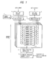
- Fig. 1 is a block diagram showing a schematic arrangement of an image signal processing apparatus according to an embodiment of the present invention.
- the apparatus shown in Fig. 1 includes a memory block 1, and the detailed arrangement of the memory block 1 will be described in detail later with reference to Fig. 2.
- the apparatus also includes a timing controller 2, a circuit 3 for coding input data, a multiplexer 4, a demultiplexer 5, a circuit 6 for decoding an encoded signal, memory units 8 constituting the memory block, a probe position controller 9 for controlling the probe scanning position, and a scanning procedure memory circuit 10 for storing probe scanning procedure data which is input prior to reproduction in a memory device of the present invention.
- the probe position controller 9 controls the probe scanning position in a reproduction mode in accordance with the recorded content of the memory circuit 10.
- Image data to be input consists of a plurality of frames.
- the "frame” is a minimum data unit of image data.
- the data is divided by the multiplexer 4 in units of frames in correspondence with the number of memory units, and the divided data are respectively distributed to the predetermined memory units in the memory block 1.
- the memory units which received the distributed image data record the data.
- the distributed data are restored by the demultiplexer 5 to an original continuous data string, and the data string is output via the circuit 6.
- a buffer function is provided to both the data input and output units, i.e., the circuits 3 and 6 so as to prevent data loss during dead time (e.g., moving time of a probe between adjacent tracks or recording regions) generated due to a mechanism in a recording or reproduction process by scanning the probe.
- the multiplexer 4 and the demultiplexer 5 are controlled by the timing controller 2.
- the memory block 1 has a feature of recording/reproducing information on/from a desired position or region on the recording medium using the scanning probe.
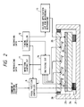
- This embodiment uses the memory block whose arrangement is shown in Fig. 2.
- the memory block will be described below with reference to Fig. 2.
- a plurality of probe electrodes 21 are respectively supported by cantilevers 22 each consisting of an elastic member, and are arranged in the vicinity of a recording medium 23.
- One memory unit is constituted by a set of one probe electrode 21 and the recording medium 23, which oppose each other.
- the recording medium 23 is supported on a supporting substrate 24, and guide grooves 25 used for selecting a recording region and realizing tracking upon scanning are formed on the surface of the medium 23.
- the probe position controller 9 is a circuit for controlling the probe/medium interval (distance in the Z direction), and probe scanning (movement and position in the X and Y directions), and is connected to driving elements 27 and 28 each comprising a piezoelectric member.
- Information is recorded on a thin film medium by an electrical method between the probe and the medium, and is reproduced by measuring a physical phenomenon caused by an approach of the probe to the medium.
- an SOAZ dye organic thin film (two-layered film) stacked on a gold electrode as a recording medium disclosed in Japanese Laid-Open Patent Application Nos. 63-161552 and 63-161553 is used as the recording medium 23.
- a recording bit is written on the medium by a pulse voltage generated by a voltage application circuit 13, a probe current is detected, and recorded image information is reproduced via a switching circuit 14 and a waveform shaping circuit 11.
- a timing controller 12 is connected to the probe position controller 9, the voltage application circuit 13 for recording/reproducing, and the switching circuit 14, and manages time sharing of data and distribution of recording signals to the probes.
- a lever-shaped multi probe unit including the probe electrodes used in this embodiment is manufactured as follows.
- a 0.3- ⁇ m thick SiO 2 film is formed on the surface of an Si substrate by thermal oxidation, and a plurality of lever shapes each having a length of 100 ⁇ m and a width of 20 ⁇ m are patterned.
- an electrical signal wiring pattern for the probe electrodes is formed, and anisotropic etching is performed using an aqueous KOH solution from the rear surface side of the substrate, thus forming cantilevers.
- 5- ⁇ m high probe electrodes 21 are formed on the tips of the levers by an electron beam deposition method of, e.g., carbon, thereby forming the multi probe unit on a probe unit substrate 26.
- the memory block manufactured, as described above, performs recording at a density of 1,920 probes, an X-direction scanning frequency of 500 Hz, a main scanning width of 1 ⁇ m, a bit diameter of 5 nm, and a bit interval of 10 nm, and has a recording/reproduction speed of 192 Mbps as a whole and 100 kHz per unit.
- an edit operation of image information in the reproduction mode can be easily performed. More specifically, as will be described below, after image data is temporarily stored in the memory block, an edit operation and reproduction output can be simultaneously realized by controlling probe scanning using a procedure and scanning regions different from those in the recording mode.
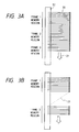
- Figs. 3A and 3B show a case wherein a certain image portion is deleted and skipped in edit processing.
- Figs. 3A and 3B respectively illustrate scanning states of a single probe on the recording medium in the recording and reproduction modes. Note that other probes are also simultaneously scanned in the same manner as the illustrated probe.
- Figs. 3A and 3B illustrate a main scanning line 30 of the probe, and an arrow 31 indicating the sub-scanning direction.
- these drawings show a guide groove 32 used for selecting a recording region, and performing tracking upon scanning.
- recording bits are formed on the recording medium while main-scanning the probe.
- the obtained image signals are temporally thinned out, thus obtaining a high-speed reproduced image.
- Figs. 3A and 3B illustrate a forward jumping operation from frame 1 to frame 3.
- the scanning region jumping operation 33 may be performed in a direction opposite to the recording order.
- an arbitrary recording region may be scanned a number of times.
- a certain image is to be repetitively output a number of times during a series of dynamic image reproduction operations, since a recorded image signal and a reproduced output signal have a one-to-one correspondence therebetween in a conventional apparatus, copying processing of an image signal is required as needed.
- the same effect as the conventional copy processing can be obtained by re-scanning the probe.
- an arbitrary frame memory region is repetitively probe-scanned for a predetermined period of time, thus obtaining a still image as an image signal to be reproduced.
- the scanning region jumping operation 33 is managed and executed by the scanning procedure memory circuit 10 and the probe position controller 9 shown in Fig. 1. These circuits will be described below with reference to Fig. 4.
- the probe position controller 9 includes a loadable up/down counter 41, a comparator 42, and a D/A converter 43.
- the scanning procedure memory circuit 10 includes tables 44 and 45 for converting a frame number into a probe address (counter value), and a table 46 which stores frame numbers of jumping origins and frame numbers of jumping destinations as a scanning region jumping condition.
- a user (editor) inputs (or records) desired scanning procedure data.
- the probe position is determined by an increase/decrease in output from the counter 41 in a normal scanning operation.
- the counter 41 loads the address value of the jumping destination in response to a signal generated by the comparator 42, and the probe moves to a desired position.
- the table 46 increments an internal pointer by one to output the next jumping condition.
- the probe position management counter is used.
- recording region address information may be described in a recording data string to be scanned by the probe, and may be read out in the reproduction mode, thereby detecting the absolute position of the probe simultaneous with reproduction of image data. This method is also suitable for the present invention.
- the scanning procedure can be stored in the recording medium. More specifically, this method acquires the address of the next recording region to be accessed by the probe simultaneously with image data, and is an application of a conventional technique for recording/reproducing a file allocation table on/from a magnetic recording medium together with a data string when data files are divisionally managed on the magnetic recording medium. In the present invention, however, an operation for rewriting only the allocation table content without changing a data string of image signals is performed for the purpose of editing reproduction information.
- the scanning region jumping condition table is separately arranged as in the above embodiment, the number of jumping operations is limited by the table capacity.
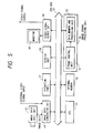
- Fig. 5 is a block diagram showing a schematic arrangement of a video camera recorder according to the second embodiment of the present invention.
- the video camera recorder includes an image data input unit 53 comprising an optical system and a CCD, and an image data conversion circuit 54 for performing a CCD driving operation, digital conversion, level conversion, and the like. Input image data is transferred to and stored in an image signal processing apparatus 50.
- the video camera recorder also includes a CPU 55 for performing data acquisition, transfer, and calculations.
- the video camera recorder comprises, as peripheral circuits of the CPU 55, the image data input unit 50, the image data conversion circuit 54, a video signal output circuit 59, an internal memory 56 as a working area, an operation panel 57 used for setting an operation condition, and externally inputting a processing command, and a display unit 58 for confirming an operation condition and state. These units are connected to a bus 61 for transferring a control signal and data.
- the capacity of the memory block used in this embodiment is about 120 Gbytes, and allows recording of a color dynamic image for about an hour. Thus, this portable compact video camera recorder has a wide application range.
- the above-mentioned image signal processing apparatus 50 has the same function as in the first embodiment.
- an instruction (procedure book) associated with a reproduction procedure is input from the operation panel, and is recorded in a probe control unit 51.
- data stored in a data memory and processing unit 52 is subjected to edit processing such as delete processing, high-speed reproduction processing, reversal reproduction processing, copy processing, still processing, and the like, and the processed data is output as a video signal to a monitor 60 and an external apparatus.
- a reproduction operation of the program by deleting only commercial portions broadcasted during the program, a reproduction operation of the program by extracting only the commercial portions, a high-speed reproduction operation (fast forward), and the like can be freely selected without being restricted by the storage capacity. Since the operation in the reproduction mode is simple, the above-mentioned function is very effective.
- image data can be edited in the recording mode. That is, attribute information corresponding to a signal to be input is recorded in the scanning procedure region (included in the probe control unit 51) simultaneously with or prior to image signal recording, and in the reproduction mode, the probe control unit 51 can determine and execute based on the attribute information whether or not the recorded signal is reproduced, and the priority order of reproduction.
- the video camera recorder comprising the image signal processing apparatus is exemplified.
- the present invention may be applied to a video recorder.
- the arrangement of the video recorder is substantially the same as that of the video camera recorder, except for some components of the image data input unit 53, and the image data conversion circuit 54, and an image signal processing apparatus having the same function as that of the image signal processing apparatus 50 can be adopted.
- a video recorder having the above-mentioned edit function can be realized as in the video camera recorder.
- an image processing apparatus which can easily obtain reproduction information subjected to edit processing such as re-arrangement of the reproduction order, partial deletion of information, and the like after image information is recorded, is obtained. Furthermore, when the apparatus has a compact memory portion, it can be assembled in a video recorder, a video camera recorder, or the like. As a result, a multi-functional, compact apparatus can be provided by adding a simple mechanism.
Landscapes
- Engineering & Computer Science (AREA)
- Chemical & Material Sciences (AREA)
- Nanotechnology (AREA)
- Multimedia (AREA)
- Signal Processing (AREA)
- Crystallography & Structural Chemistry (AREA)
- Life Sciences & Earth Sciences (AREA)
- Mathematical Physics (AREA)
- Health & Medical Sciences (AREA)
- Physics & Mathematics (AREA)
- General Health & Medical Sciences (AREA)
- Molecular Biology (AREA)
- Theoretical Computer Science (AREA)
- Television Signal Processing For Recording (AREA)
- Signal Processing For Digital Recording And Reproducing (AREA)
- Holo Graphy (AREA)
- Apparatus For Radiation Diagnosis (AREA)
- Auxiliary Devices For Music (AREA)
- Image Analysis (AREA)
- Image Processing (AREA)
Claims (2)
- Appareil de traitement de signal d'image destiné à mémoriser temporairement de l'information d'image et à sortir l'information après traitement de signal, comprenant :chacun desdits modules de mémoire incluant :un moyen (4) de division destiné à diviser l'information d'image d'entrée ; etun moyen de mémorisation comprenant plusieurs modules (8) de mémoire correspondant en nombre au nombre de divisions de ladite information d'image d'entrée, chaque module (8) de mémoire étant destiné à mémoriser une partie de l'information divisée,ledit moyen de mémorisation incluant :une électrode de sonde (21) ;un support (23) d'enregistrement disposé de façon à faire face à ladite électrode (21) de sonde ;caractérisé en ce que :un moyen de balayage destiné à déplacer les électrodes (21) de sonde desdits modules de mémorisation par rapport audit support (23) d'enregistrement de façon que lesdites électrodes (21) de sonde balayent une surface dudit support (23) d'enregistrement ; etun moyen (13) d'application de tension destiné à appliquer, entre ledit support (23) d'enregistrement et chacune desdites électrodes (21) de sonde, une tension appropriée pour enregistrement de l'information d'image sur ledit support (23) d'enregistrement en face desdites sondes (21), et à appliquer, entre ledit support (23) d'enregistrement et chacune desdites électrodes (21) de sonde, une tension appropriée pour la reproduction de l'information d'image enregistrée sur ledit support d'enregistrement ; etun moyen (9) de commande destiné à commander ledit moyen de balayage dudit moyen de mémorisation de façon à entrer et sortir l'information d'image,
ledit moyen de mémorisation comprend une mémoire (10) pouvant être réécrite, destinée à mémoriser une procédure de mise en oeuvre desdites électrodes (21) de sonde, ladite procédure de mise en oeuvre pouvant être définie par un utilisateur, ladite procédure de mise en oeuvre étant destinée à être utilisée par ledit moyen (9) de commande pour commander ledit moyen de balayage pour utiliser une procédure de reproduction différente de la procédure d'écriture, en mettant ainsi en forme ladite information d'image pendant la reproduction. - Enregistreur pour caméra vidéo destiné à entrer/sortir de l'information d'image comprenant :chacun desdits modules de mémoire incluant :un moyen (53) d'entrée d'image ;un moyen (4) de division destiné à diviser l'information d'image entrée par ledit moyen (53) d'entrée d'image ;un moyen (52) de mémorisation comprenant plusieurs modules (8) de mémoire correspondant en nombre au nombre de divisions de ladite information d'image d'entrée, chaque module (8) de mémoire étant destiné à mémoriser une partie de l'information divisée,ledit moyen de mémorisation incluant :une électrode de sonde (21) ;un support (23) d'enregistrement disposé de façon à faire face à ladite électrode (21) de sonde ;caractérisé en ce que :un moyen de balayage destiné à déplacer les électrodes (21) de sonde desdits modules de mémorisation par rapport audit support (23) d'enregistrement de façon que lesdites électrodes (21) de sonde balayent une surface dudit support (23) d'enregistrement ; etun moyen (13) d'application de tension destiné à appliquer, entre ledit support (23) d'enregistrement et chacune desdites électrodes (21) de sonde, une tension appropriée pour enregistrement de l'information d'image sur ledit support (23) d'enregistrement en face desdites sondes (21), et à appliquer, entre ledit support (23) d'enregistrement et chacune desdites électrodes (21) de sonde, une tension appropriée pour la reproduction de l'information d'image enregistrée sur ledit support d'enregistrement ; etun moyen (9) de commande destiné à commander ledit moyen de balayage dudit moyen (53) de mémorisation de façon à entrer et sortir l'information d'image,
ledit moyen (52) de mémorisation comprend une mémoire (10) pouvant être réécrite, destinée à mémoriser une procédure de mise en oeuvre desdites électrodes (21) de sonde, ladite procédure de mise en oeuvre pouvant être définie par un utilisateur, ladite procédure de mise en oeuvre étant destinée à être utilisée par ledit moyen (9) de commande pour commander ledit moyen de balayage pour utiliser une procédure de reproduction différente de la procédure d'écriture, en mettant ainsi en forme ladite information d'image pendant la reproduction.
Applications Claiming Priority (2)
| Application Number | Priority Date | Filing Date | Title |
|---|---|---|---|
| JP340753/92 | 1992-12-21 | ||
| JP4340753A JPH06195772A (ja) | 1992-12-21 | 1992-12-21 | 画像信号処理機構およびその適用機器 |
Publications (3)
| Publication Number | Publication Date |
|---|---|
| EP0603705A2 EP0603705A2 (fr) | 1994-06-29 |
| EP0603705A3 EP0603705A3 (fr) | 1994-12-14 |
| EP0603705B1 true EP0603705B1 (fr) | 1999-03-03 |
Family
ID=18339979
Family Applications (1)
| Application Number | Title | Priority Date | Filing Date |
|---|---|---|---|
| EP93120085A Expired - Lifetime EP0603705B1 (fr) | 1992-12-21 | 1993-12-13 | Appareil de traitement d'un signal d'image |
Country Status (6)
| Country | Link |
|---|---|
| US (1) | US5778134A (fr) |
| EP (1) | EP0603705B1 (fr) |
| JP (1) | JPH06195772A (fr) |
| AT (1) | ATE177276T1 (fr) |
| CA (1) | CA2111769C (fr) |
| DE (1) | DE69323705T2 (fr) |
Families Citing this family (18)
| Publication number | Priority date | Publication date | Assignee | Title |
|---|---|---|---|---|
| EP0648049A1 (fr) * | 1993-10-08 | 1995-04-12 | Hitachi, Ltd. | Procédé et appareil d'enregistrement et reproduction d'information |
| JP3912814B2 (ja) * | 1996-02-15 | 2007-05-09 | キヤノン株式会社 | 情報処理装置 |
| US7304486B2 (en) * | 1998-07-08 | 2007-12-04 | Capres A/S | Nano-drive for high resolution positioning and for positioning of a multi-point probe |
| US7260051B1 (en) | 1998-12-18 | 2007-08-21 | Nanochip, Inc. | Molecular memory medium and molecular memory integrated circuit |
| US6982898B2 (en) * | 2002-10-15 | 2006-01-03 | Nanochip, Inc. | Molecular memory integrated circuit utilizing non-vibrating cantilevers |
| US20040150472A1 (en) * | 2002-10-15 | 2004-08-05 | Rust Thomas F. | Fault tolerant micro-electro mechanical actuators |
| US7233517B2 (en) | 2002-10-15 | 2007-06-19 | Nanochip, Inc. | Atomic probes and media for high density data storage |
| US6985377B2 (en) * | 2002-10-15 | 2006-01-10 | Nanochip, Inc. | Phase change media for high density data storage |
| US7471552B2 (en) * | 2003-08-04 | 2008-12-30 | Ovonyx, Inc. | Analog phase change memory |
| US7522132B2 (en) * | 2004-03-17 | 2009-04-21 | Canon Kabushiki Kaisha | Image display apparatus |
| US7301887B2 (en) * | 2004-04-16 | 2007-11-27 | Nanochip, Inc. | Methods for erasing bit cells in a high density data storage device |
| US7379412B2 (en) | 2004-04-16 | 2008-05-27 | Nanochip, Inc. | Methods for writing and reading highly resolved domains for high density data storage |
| US20050232061A1 (en) | 2004-04-16 | 2005-10-20 | Rust Thomas F | Systems for writing and reading highly resolved domains for high density data storage |
| US7463573B2 (en) | 2005-06-24 | 2008-12-09 | Nanochip, Inc. | Patterned media for a high density data storage device |
| US7367119B2 (en) | 2005-06-24 | 2008-05-06 | Nanochip, Inc. | Method for forming a reinforced tip for a probe storage device |
| US7309630B2 (en) | 2005-07-08 | 2007-12-18 | Nanochip, Inc. | Method for forming patterned media for a high density data storage device |
| US7514942B2 (en) * | 2006-09-27 | 2009-04-07 | Intel Corporation | Probe based patterning of microelectronic and micromechanical devices |
| RU2479937C2 (ru) * | 2007-03-30 | 2013-04-20 | Сони Корпорейшн | Устройство и способ обработки информации |
Family Cites Families (14)
| Publication number | Priority date | Publication date | Assignee | Title |
|---|---|---|---|---|
| JPS5765967A (en) * | 1980-10-13 | 1982-04-21 | Trio Kenwood Corp | Method for reproducing video disc |
| US4361849A (en) * | 1980-11-06 | 1982-11-30 | Rca Corporation | Video disc vari-speed playback system |
| US5260837A (en) * | 1980-11-21 | 1993-11-09 | Lemelson Jerome H | Portable television camera-recorder and method for operating same |
| DE3225238C2 (de) * | 1981-07-06 | 1984-12-13 | Victor Company Of Japan, Ltd., Yokohama, Kanagawa | Wiedergabegerät für ein rotierbares Aufzeichnungsmedium |
| JPS6022885A (ja) * | 1983-07-18 | 1985-02-05 | Matsushita Electric Ind Co Ltd | 電子スチルカメラの再生装置 |
| GB8408113D0 (en) * | 1984-03-29 | 1984-05-10 | Quantel Ltd | Video editing/viewing systems |
| US5214515A (en) * | 1986-10-28 | 1993-05-25 | Mitsubishi Denki Kabushiki Kaisha | Video signal recording/reproducing apparatus |
| US4906840A (en) * | 1988-01-27 | 1990-03-06 | The Board Of Trustees Of Leland Stanford Jr., University | Integrated scanning tunneling microscope |
| US4970608A (en) * | 1988-03-18 | 1990-11-13 | Olympus Optical Co., Ltd. | Editing system for rearranging allocation of information units on an information recording medium |
| EP0382192B1 (fr) * | 1989-02-09 | 1993-08-18 | Olympus Optical Co., Ltd. | Appareil mémoire avec microscope tunnel à balayage |
| KR920005598A (ko) * | 1990-08-29 | 1992-03-28 | 오가 노리오 | 디지탈 전자스틸카메라 |
| JP3126409B2 (ja) * | 1991-06-05 | 2001-01-22 | キヤノン株式会社 | 情報記録再生方法 |
| JP3109861B2 (ja) * | 1991-06-12 | 2000-11-20 | キヤノン株式会社 | 情報の記録及び/又は再生装置 |
| JP2794348B2 (ja) * | 1991-06-21 | 1998-09-03 | キヤノン株式会社 | 記録媒体、その製造方法、情報処理装置 |
-
1992
- 1992-12-21 JP JP4340753A patent/JPH06195772A/ja active Pending
-
1993
- 1993-12-13 DE DE69323705T patent/DE69323705T2/de not_active Expired - Fee Related
- 1993-12-13 EP EP93120085A patent/EP0603705B1/fr not_active Expired - Lifetime
- 1993-12-13 AT AT93120085T patent/ATE177276T1/de active
- 1993-12-17 CA CA002111769A patent/CA2111769C/fr not_active Expired - Fee Related
-
1996
- 1996-09-03 US US08/711,306 patent/US5778134A/en not_active Expired - Lifetime
Also Published As
| Publication number | Publication date |
|---|---|
| EP0603705A2 (fr) | 1994-06-29 |
| DE69323705T2 (de) | 1999-07-22 |
| CA2111769C (fr) | 1999-03-30 |
| CA2111769A1 (fr) | 1994-06-22 |
| EP0603705A3 (fr) | 1994-12-14 |
| ATE177276T1 (de) | 1999-03-15 |
| JPH06195772A (ja) | 1994-07-15 |
| US5778134A (en) | 1998-07-07 |
| DE69323705D1 (de) | 1999-04-08 |
Similar Documents
| Publication | Publication Date | Title |
|---|---|---|
| EP0603705B1 (fr) | Appareil de traitement d'un signal d'image | |
| US5526334A (en) | Information processing apparatus with multiple probes and method therefor | |
| US5373494A (en) | Information recording and/or reproducing apparatus | |
| EP0382062A2 (fr) | Circuits électroniques incluant une sonde atomique | |
| EP0541978B1 (fr) | Appareil de traitement d'information | |
| JPH06197290A (ja) | デジタルテレビジョン受像機 | |
| JP3029143B2 (ja) | 情報再生方法 | |
| JP3912814B2 (ja) | 情報処理装置 | |
| JP3129860B2 (ja) | 画像信号処理機構およびその適用機器 | |
| US5581364A (en) | Method for recording and/or reproducing image signals and an apparatus therefor utilizing two dimensional scanning of a recording medium by a probe | |
| JP2930454B2 (ja) | 記録及び/又は再生装置 | |
| JP3039725B2 (ja) | 情報処理装置 | |
| JP3014855B2 (ja) | 記録情報再生装置 | |
| JPH0744907A (ja) | 情報記録再生装置 | |
| JPH0785510A (ja) | 情報記録再生装置 | |
| JP3095915B2 (ja) | 情報処理装置 | |
| JPH0744908A (ja) | 情報記録再生装置 | |
| JP3074917B2 (ja) | トンネル電流メモリ再生装置 | |
| JP3078161B2 (ja) | 記録再生装置 | |
| KR100842890B1 (ko) | 탐침 또는 전도성 구조를 이용한 강유전층의 비트 기록 방법 | |
| JP2000113532A (ja) | 情報再生装置および情報再生方法 | |
| JP2000011473A (ja) | 記録再生装置における面合わせ方法及び機構 | |
| JPH08221817A (ja) | 情報処理装置 | |
| JPH06119665A (ja) | 情報記録再生装置 | |
| JPH04125830A (ja) | 情報記録担体と情報記録及び/又は再生装置と情報記録及び/又は再生方法 |
Legal Events
| Date | Code | Title | Description |
|---|---|---|---|
| PUAI | Public reference made under article 153(3) epc to a published international application that has entered the european phase |
Free format text: ORIGINAL CODE: 0009012 |
|
| AK | Designated contracting states |
Kind code of ref document: A2 Designated state(s): AT BE CH DE DK ES FR GB GR IT LI LU NL PT SE |
|
| PUAL | Search report despatched |
Free format text: ORIGINAL CODE: 0009013 |
|
| AK | Designated contracting states |
Kind code of ref document: A3 Designated state(s): AT BE CH DE DK ES FR GB GR IT LI LU NL PT SE |
|
| 17P | Request for examination filed |
Effective date: 19950614 |
|
| 17Q | First examination report despatched |
Effective date: 19970402 |
|
| GRAG | Despatch of communication of intention to grant |
Free format text: ORIGINAL CODE: EPIDOS AGRA |
|
| GRAG | Despatch of communication of intention to grant |
Free format text: ORIGINAL CODE: EPIDOS AGRA |
|
| GRAH | Despatch of communication of intention to grant a patent |
Free format text: ORIGINAL CODE: EPIDOS IGRA |
|
| GRAH | Despatch of communication of intention to grant a patent |
Free format text: ORIGINAL CODE: EPIDOS IGRA |
|
| GRAA | (expected) grant |
Free format text: ORIGINAL CODE: 0009210 |
|
| AK | Designated contracting states |
Kind code of ref document: B1 Designated state(s): AT BE CH DE DK ES FR GB GR IT LI LU NL PT SE |
|
| PG25 | Lapsed in a contracting state [announced via postgrant information from national office to epo] |
Ref country code: SE Free format text: THE PATENT HAS BEEN ANNULLED BY A DECISION OF A NATIONAL AUTHORITY Effective date: 19990303 Ref country code: NL Free format text: LAPSE BECAUSE OF FAILURE TO SUBMIT A TRANSLATION OF THE DESCRIPTION OR TO PAY THE FEE WITHIN THE PRESCRIBED TIME-LIMIT Effective date: 19990303 Ref country code: LI Free format text: LAPSE BECAUSE OF FAILURE TO SUBMIT A TRANSLATION OF THE DESCRIPTION OR TO PAY THE FEE WITHIN THE PRESCRIBED TIME-LIMIT Effective date: 19990303 Ref country code: GR Free format text: LAPSE BECAUSE OF NON-PAYMENT OF DUE FEES Effective date: 19990303 Ref country code: ES Free format text: THE PATENT HAS BEEN ANNULLED BY A DECISION OF A NATIONAL AUTHORITY Effective date: 19990303 Ref country code: CH Free format text: LAPSE BECAUSE OF FAILURE TO SUBMIT A TRANSLATION OF THE DESCRIPTION OR TO PAY THE FEE WITHIN THE PRESCRIBED TIME-LIMIT Effective date: 19990303 Ref country code: BE Free format text: LAPSE BECAUSE OF FAILURE TO SUBMIT A TRANSLATION OF THE DESCRIPTION OR TO PAY THE FEE WITHIN THE PRESCRIBED TIME-LIMIT Effective date: 19990303 Ref country code: AT Free format text: LAPSE BECAUSE OF FAILURE TO SUBMIT A TRANSLATION OF THE DESCRIPTION OR TO PAY THE FEE WITHIN THE PRESCRIBED TIME-LIMIT Effective date: 19990303 |
|
| REF | Corresponds to: |
Ref document number: 177276 Country of ref document: AT Date of ref document: 19990315 Kind code of ref document: T |
|
| REG | Reference to a national code |
Ref country code: CH Ref legal event code: EP |
|
| ET | Fr: translation filed | ||
| REF | Corresponds to: |
Ref document number: 69323705 Country of ref document: DE Date of ref document: 19990408 |
|
| ITF | It: translation for a ep patent filed | ||
| PG25 | Lapsed in a contracting state [announced via postgrant information from national office to epo] |
Ref country code: DK Free format text: LAPSE BECAUSE OF FAILURE TO SUBMIT A TRANSLATION OF THE DESCRIPTION OR TO PAY THE FEE WITHIN THE PRESCRIBED TIME-LIMIT Effective date: 19990603 |
|
| PG25 | Lapsed in a contracting state [announced via postgrant information from national office to epo] |
Ref country code: PT Free format text: LAPSE BECAUSE OF FAILURE TO SUBMIT A TRANSLATION OF THE DESCRIPTION OR TO PAY THE FEE WITHIN THE PRESCRIBED TIME-LIMIT Effective date: 19990604 |
|
| NLV1 | Nl: lapsed or annulled due to failure to fulfill the requirements of art. 29p and 29m of the patents act | ||
| REG | Reference to a national code |
Ref country code: CH Ref legal event code: PL |
|
| PG25 | Lapsed in a contracting state [announced via postgrant information from national office to epo] |
Ref country code: LU Free format text: LAPSE BECAUSE OF NON-PAYMENT OF DUE FEES Effective date: 19991213 |
|
| PLBE | No opposition filed within time limit |
Free format text: ORIGINAL CODE: 0009261 |
|
| STAA | Information on the status of an ep patent application or granted ep patent |
Free format text: STATUS: NO OPPOSITION FILED WITHIN TIME LIMIT |
|
| 26N | No opposition filed | ||
| REG | Reference to a national code |
Ref country code: GB Ref legal event code: IF02 |
|
| PGFP | Annual fee paid to national office [announced via postgrant information from national office to epo] |
Ref country code: GB Payment date: 20041208 Year of fee payment: 12 Ref country code: FR Payment date: 20041208 Year of fee payment: 12 |
|
| PGFP | Annual fee paid to national office [announced via postgrant information from national office to epo] |
Ref country code: DE Payment date: 20041209 Year of fee payment: 12 |
|
| PG25 | Lapsed in a contracting state [announced via postgrant information from national office to epo] |
Ref country code: IT Free format text: LAPSE BECAUSE OF NON-PAYMENT OF DUE FEES;WARNING: LAPSES OF ITALIAN PATENTS WITH EFFECTIVE DATE BEFORE 2007 MAY HAVE OCCURRED AT ANY TIME BEFORE 2007. THE CORRECT EFFECTIVE DATE MAY BE DIFFERENT FROM THE ONE RECORDED. Effective date: 20051213 Ref country code: GB Free format text: LAPSE BECAUSE OF NON-PAYMENT OF DUE FEES Effective date: 20051213 |
|
| PG25 | Lapsed in a contracting state [announced via postgrant information from national office to epo] |
Ref country code: DE Free format text: LAPSE BECAUSE OF NON-PAYMENT OF DUE FEES Effective date: 20060701 |
|
| GBPC | Gb: european patent ceased through non-payment of renewal fee |
Effective date: 20051213 |
|
| PG25 | Lapsed in a contracting state [announced via postgrant information from national office to epo] |
Ref country code: FR Free format text: LAPSE BECAUSE OF NON-PAYMENT OF DUE FEES Effective date: 20060831 |
|
| REG | Reference to a national code |
Ref country code: FR Ref legal event code: ST Effective date: 20060831 |