EP0604006A2 - Flüssigkristallzelle mit aktiver Matrix - Google Patents
Flüssigkristallzelle mit aktiver Matrix Download PDFInfo
- Publication number
- EP0604006A2 EP0604006A2 EP93308546A EP93308546A EP0604006A2 EP 0604006 A2 EP0604006 A2 EP 0604006A2 EP 93308546 A EP93308546 A EP 93308546A EP 93308546 A EP93308546 A EP 93308546A EP 0604006 A2 EP0604006 A2 EP 0604006A2
- Authority
- EP
- European Patent Office
- Prior art keywords
- liquid crystal
- crystal display
- active matrix
- matrix liquid
- display cell
- Prior art date
- Legal status (The legal status is an assumption and is not a legal conclusion. Google has not performed a legal analysis and makes no representation as to the accuracy of the status listed.)
- Granted
Links
Images



Classifications
-
- G—PHYSICS
- G02—OPTICS
- G02F—OPTICAL DEVICES OR ARRANGEMENTS FOR THE CONTROL OF LIGHT BY MODIFICATION OF THE OPTICAL PROPERTIES OF THE MEDIA OF THE ELEMENTS INVOLVED THEREIN; NON-LINEAR OPTICS; FREQUENCY-CHANGING OF LIGHT; OPTICAL LOGIC ELEMENTS; OPTICAL ANALOGUE/DIGITAL CONVERTERS
- G02F1/00—Devices or arrangements for the control of the intensity, colour, phase, polarisation or direction of light arriving from an independent light source, e.g. switching, gating or modulating; Non-linear optics
- G02F1/01—Devices or arrangements for the control of the intensity, colour, phase, polarisation or direction of light arriving from an independent light source, e.g. switching, gating or modulating; Non-linear optics for the control of the intensity, phase, polarisation or colour
- G02F1/13—Devices or arrangements for the control of the intensity, colour, phase, polarisation or direction of light arriving from an independent light source, e.g. switching, gating or modulating; Non-linear optics for the control of the intensity, phase, polarisation or colour based on liquid crystals, e.g. single liquid crystal display cells
- G02F1/133—Constructional arrangements; Operation of liquid crystal cells; Circuit arrangements
- G02F1/136—Liquid crystal cells structurally associated with a semi-conducting layer or substrate, e.g. cells forming part of an integrated circuit
- G02F1/1362—Active matrix addressed cells
- G02F1/136213—Storage capacitors associated with the pixel electrode
-
- G—PHYSICS
- G02—OPTICS
- G02F—OPTICAL DEVICES OR ARRANGEMENTS FOR THE CONTROL OF LIGHT BY MODIFICATION OF THE OPTICAL PROPERTIES OF THE MEDIA OF THE ELEMENTS INVOLVED THEREIN; NON-LINEAR OPTICS; FREQUENCY-CHANGING OF LIGHT; OPTICAL LOGIC ELEMENTS; OPTICAL ANALOGUE/DIGITAL CONVERTERS
- G02F1/00—Devices or arrangements for the control of the intensity, colour, phase, polarisation or direction of light arriving from an independent light source, e.g. switching, gating or modulating; Non-linear optics
- G02F1/01—Devices or arrangements for the control of the intensity, colour, phase, polarisation or direction of light arriving from an independent light source, e.g. switching, gating or modulating; Non-linear optics for the control of the intensity, phase, polarisation or colour
- G02F1/13—Devices or arrangements for the control of the intensity, colour, phase, polarisation or direction of light arriving from an independent light source, e.g. switching, gating or modulating; Non-linear optics for the control of the intensity, phase, polarisation or colour based on liquid crystals, e.g. single liquid crystal display cells
- G02F1/133—Constructional arrangements; Operation of liquid crystal cells; Circuit arrangements
- G02F1/1333—Constructional arrangements; Manufacturing methods
- G02F1/1335—Structural association of cells with optical devices, e.g. polarisers or reflectors
- G02F1/133509—Filters, e.g. light shielding masks
- G02F1/133512—Light shielding layers, e.g. black matrix
Definitions
- the present invention relates to an active matrix liquid crystal display cell which serves to provide a single picture element, namely, a pixel, and an active matrix liquid crystal display panel comprising a plurality of the active matrix liquid crystal display cells arranged in a matrix fashion.
- a conventional active matrix liquid crystal display cell of the type described comprises a switching active element for driving liquid crystal, a capacitance element which stores charge for driving the liquid crystal, a pair of transparent electrodes the space between which is filled with the liquid crystal, and a shading layer for protecting the switching active element and enhancing the contrast of the image.
- each of the active matrix liquid crystal display cells becomes small in size so as to increase numbers thereof for getting an excellent resolution power of the active matrix liquid crystal display panel.
- the conventional active matrix liquid crystal display panel cannot provide a bright image, due to a structure of each active matrix liquid crystal display cell, when the active matrix liquid crystal display cell is small in size.
- an active matrix liquid crystal display cell comprising: a switching active element; first and second transparent electrodes between which liquid crystal is disposed, said first transparent electrode being connected to said switching active element for driving said liquid crystal and said second transparent electrode being positioned opposite to said first transparent electrode; a shading layer which is made of a conductive material, and is disposed partially under the first transparent electrode; and an insulating layer which is interposed between said shading layer and said first transparent electrode.
- the shading layer may be made of aluminum and the insulating layer may be formed by an anodic oxidation of the aluminum.
- an active matrix liquid crystal display panel comprising a plurality of active matrix liquid crystal display cells arranged in a matrix fashion, each of the active matrix liquid crystal display cells being as set forth above.
- a conventional active matrix liquid crystal display cell will first be described for a better understanding of this invention.
- the conventional active matrix liquid crystal display cell 100 comprises a principal glass substrate 102, an opposite glass substrate 104, a transparent pixel electrode 106 deposited at the side of the principal glass substrate 102, a transparent opposite electrode 108 formed under the whole area of the opposite glass substrate 104, and a liquid crystal 110 filling the space between the transparent pixel electrode 106 and the transparent opposite electrode 108, a switching active element 120, a capacitance element 130, and a shading layer 140.
- the switching active element 120 is formed by a thin-film transistor (TFT) of a bottom gate type, which consists of a gate 121, a gate insulating layer 122, an armorphous silicon layer 123, a doped amorphous silicon layer 124, a drain 125, and a source 126.
- the gate 121 is connected to a gate bus (not shown) and the drain 125 is connected to a drain or signal bus (not shown), while the source 126 is connected to the transparent pixel electrode 106.
- the capacitance element 130 consists of the transparent pixel electrode 106, a transparent electrode 132, and a dielectric layer 134 which is defined by a portion of the gate insulating layer 122.
- the shading layer 140 is partially deposited under the transparent opposite electrode 108.
- the liquid crystal 110 also fills the space between the switching active element 220 and the shading layer 140, as illustrated in Fig. 1.
- the transparent pixel electrode 106, the transparent electrode 132 and the transparent opposite electrode 108 are formed from ITO (Indium Tin Oxide) layer.
- a plurality of the active matrix liquid crystal display cells 100 are arranged in a matrix fashion to form an active matrix liquid crystal display panel (not shown).
- each active matrix liquid crystal display cell 100 is sometimes decreased in size to 50 x 50 micron meters.
- the shading layer 140 since the shading layer 140 is deposited at the side of the opposite glass substrate 104, the shading layer 140 must be fully expanded to cover the whole area of the switching active element 120 and an edge portion of the transparent pixel electrode 106 in order to completely protect the switching active element 120 from light and to prevent a leak of light around the transparent electrode 132.
- an allowance of about 10 micron meters is generally required when the opposite glass substrate 104 is positioned to be fitted to the principal glass substrate 102. Further, an overlap of approximately 5 micron meters is required between the transparent electrode 132 and the shading layer 140. Accordingly, an allowance of about 15 micron meters is required at each side of the active matrix liquid crystal display cell 100. Thus a total allowance of 30 micron meters is required at both sides of the active matrix liquid crystal display cell 100, so in the case of a cell of 50 x 50 micron meters the effective pixel portion is only 20 x 20 micron meters. Thus, it is difficult to utilize light efficiency.
- the capacitance element 130 is formed by the transparent pixel electrode 106 and the transparent electrode 132 both of which are made of ITO and between which the dielectric layer 134 is interposed. Since the transmittance of the each ITO layer is about 90%, the overall transmittance is about 80% when light is transmitted through the transparent pixel electrode 106 as well as the transparent opposite electrode 108. Furthermore, since the transparent electrode 132 has a poor conductivity, it is necessary that the gate 121' is connected to wiring (not shown) having low resistance. If the width of the gate 121' is 5 micron meters, the above-mentioned effective pixel portion further reduces to 15 x 20 micron meters.
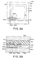
- FIGs. 2, 3A and 3B there is described an active matrix liquid crystal display cell and an active matrix liquid crystal display panel comprising a plurality of the active matrix liquid crystal display cells according to a first embodiment of this invention.
- an active matrix liquid crystal display panel 200 comprises a plurality of active matrix liquid crystal display cells 30 which are arranged in a matrix fashion, signal buses 150, and gate buses 152.
- each of the active matrix liquid crystal display cells 300 comprises a principal transparent glass substrate 302 having a principal surface 302a directed upwards of Fig. 3B, an opposite transparent glass substrate 304 having a lower surface 304a directed downwards of Fig. 3B, a thin-film transistor (TFT) 306 of top-gate type which is formed on the principal surface 302a, a first transparent electrode 308 connected to the TFT 306 for driving liquid crystal, a second transparent electrode 310 which is formed on the lower surface 304a and which is positioned opposite to the first transparent electrode 308, a shading layer 312 which is made of aluminum, and an insulating layer 314 which is formed by an anodic oxidation of aluminum.
- TFT thin-film transistor
- the shading layer 312 may alternatively be made of the other materials having a low transmittance.
- the principal transparent glass substrate 302 and the opposite transparent glass substrate 304 are made of quartz glass.
- the TFT 306 serves as a switching active element, which comprises a polycrystalline silicon layer 306a, a gate insulating layer 306b, a gate 306c, a drain 306d, and a source 306e.
- the drain 306d is connected to the signal buses 150, while the gate 306c is connected to the gate buses 152.
- a liquid crystal 316 fills the space between the first transparent electrode 308 and the second transparent electrode 310.
- the shading layer 312 has an upper and a side surfaces 312a and 312b.
- the insulating layer 314 is formed on the upper and the side surfaces 312a and 312b by the above-mentioned anodic oxidation of aluminum.
- the insulating layer 314 is therefore made of Al2O3.
- the insulating layer 314 has a thickness between 100 and 200 nm.
- an aluminum lamina is deposited in a known manner on a surface of an inter-electrodes insulating layer 315 to be patterned into the shading layer 312 having a predetermined pattern.
- the shading layer 312 is then anodically oxidized to have the insulating layer 314 of Al2O3 on its upper and side surfaces 312a and 312b.
- the insulating layer 314 is interposed between the shading layer 312 and the first transparent electrode 308 with the shading layer 312 partially laid under the first transparent electrode 308 through the insulating layer 314.
- a capacitance element 400 is defined by the shading layer 312, the first transparent electrode 308, and the insulating layer interposed therebetween.
- an overlapping area of the shading layer 312 and the first transparent electrode 308 need to have a width between 4 and 8 micron meters.
- the portion where the source 306e is connected to the first transparent electrode 308 can not be covered by the shading layer 312, as illustrated in Fig. 3B. Accordingly, the source 306e serves as a shading layer at this portion.
- two capacitance elements 400 and 410 are formed in parallel.
- One comprises the first transparent electrode 308, the second transparent electrode 310, and the liquid crystal 316 filled therebetween, while another comprises the first transparent electrode 308, the shading layer 312, and the insulating layer 314 interposed therebetween.
- Bias voltages V1 and V2 are applied to the capacitance elements 400 and 410, respectively
- the insulating layer 314 is formed by the anodic oxidation method, there are less defects, such as pin holes or the like, in the insulating layer 314 than that formed by the other method carried out on a lower temperature condition, for example, a plasma CVD, sputtering, or the like. Consequently, the capacitance element 410 having a large dielectric area can be fabricated in a good yield.
- the active matrix liquid crystal display cell according to the second embodiment has a structure similar to that of the first embodiment except that the insulating layer 314 comprises primary and secondary insulating layers 314A and 314B.
- the primary insulating layer 314A is formed by an anodic oxidation of the shading layer 312, and thus is made of Al2O3, while the secondary insulating layer 314B is formed in another manner, for example the plasma CVD method.
- the primary insulating layer 314A of Al2O3 is formed by the anodic oxidation of the shading layer 312 to have a thickness of 100 nm
- the secondary insulating layer 314B of silicon nitride is formed by plasma CVD method to have a thickness of 100 nm.
- the insulating layer 314 comprises two stacked layers, namely, primary and secondary insulating layers 314A and 314B, it becomes possible that the above-mentioned defects, such as pin holes, in the insulating layer 314 is decreased in number, compared with the above-described first embodiment.
- the active matrix liquid crystal display cells according to the third embodiment and the modification have structures similar to that of the first and the second embodiments except that the anodic oxidation method is not used to fabricate those insulating layers.
- a single insulating layer 314' is formed on the shading layer 312.
- the insulating layer 314' is made of silicon nitride and formed by a plasma CVD method to have a thickness of, for example, 200 nm.
- double insulating layers 314'A and 314'B are formed on the shading layer 312.
- the insulating layer 314'A is made of silicon nitride and formed by a plasma CVD method to have a thickness of, for example, 100nm.
- the insulating layer 314'B is made of silicon oxide and formed by a sputtering to have a thickness of, for example, 100nm.
- the active matrix liquid crystal display cell according to the fourth embodiment has a structure similar to that of the first embodiment except that the shading layer 312 comprises double layers, one of which is a shading layer 312A of aluminum and another of which is a shading layer 312B of tantalum overlaid on the shading layer 312A.
- the shading layer 312B of tantalum is readily oxidized by the anodic oxidation to have an insulating layer 320 of Ta2O5 which has a high dielectric constant. Accordingly, another insulating layer 321 of aluminum is formed on the side surfaces of the shading layer 312A.
- the insulating layer 321 of aluminum is used to enhance a shading effect.
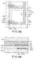
- FIGs. 9A and 9B there is described an active matrix liquid crystal display cell according to a fifth embodiment of this invention.
- the active matrix liquid crystal display cell according to the fifth embodiment has a structure similar to that of the first embodiment except that the active matrix liquid crystal display cell further comprises an additional capacitance element.
- the active matrix liquid crystal display cell 300' further comprises the additional capacitance element 330 which is positioned under the overlapping section of the first transparent electrode 308 and the shading layer 312 through an insulating layer 314.
- the additional capacitance element 330 is defined by a polycrystalline silicon layer 330a, a gate insulating layer 330b, and a gate 330c.
- the gate 330c is electrically connected to the gate buses 152.
- the polycrystalline silicon layer 330a is connected to the polycrystalline silicon layer 306a.
- a polycrystalline silicon lamina is, at first, formed on the principal transparent glass substrate 302.
- the polycrystalline silicon lamina is then patterned to a predetermined shape to form a patterned polycrystalline silicon layer.
- the gate insulating layer 330b is deposited on the patterned polycrystalline silicon layer.
- a section of the patterned polycrystalline silicon layer overlaid by the gate 330c is doped by an ion implantation method to form the polycrystalline silicon layer 330a.
- the additional capacitance element 330 is positioned under the overlapping section of the first transparent electrode 308 and the shading layer 312 through which light cannot pass originally. Accordingly, the additional capacitance element 330 makes it possible that the storage capacitance is greatly improved without reducing the efficient use of the light.
- the additional capacitance element 330 is also formed in parallel to the two capacitance elements 400 and 410 which were mentioned in respect of the first embodiment, as symbolized in Fig. 4.
- the additional capacitance element 330 is connected between the source 306e of a transistor Q1 and the gate 306c of a transistor Q2 as symbolized in Fig. 10.
- a TFT generally cannot avoid a leakage current between 0.1 pA and 1.0 pA. It is therefore desired that the storage capacitance is large enough to store a signal voltage without reduction while the active matrix liquid crystal display cell is scanned.
- the storage capacitance by the two capacitance elements 400 and 410 is 100 pF, at the most.
- the capacitance of 100 pF is not enough to store the signal voltage, as mentioned above, in view of the aforesaid leakage current of the TFT. Accordingly, it is very advantageous that the active matrix liquid crystal display cell 300' according to this embodiment comprises the additional capacitance element 330.
Landscapes
- Physics & Mathematics (AREA)
- Nonlinear Science (AREA)
- Engineering & Computer Science (AREA)
- Crystallography & Structural Chemistry (AREA)
- Mathematical Physics (AREA)
- Chemical & Material Sciences (AREA)
- Microelectronics & Electronic Packaging (AREA)
- Power Engineering (AREA)
- General Physics & Mathematics (AREA)
- Optics & Photonics (AREA)
- Liquid Crystal (AREA)
- Liquid Crystal Display Device Control (AREA)
- Thin Film Transistor (AREA)
Applications Claiming Priority (3)
| Application Number | Priority Date | Filing Date | Title |
|---|---|---|---|
| JP288039/92 | 1992-10-27 | ||
| JP28803992 | 1992-10-27 | ||
| JP28803992A JP2924506B2 (ja) | 1992-10-27 | 1992-10-27 | アクティブマトリックス型液晶表示装置の画素構造 |
Publications (3)
| Publication Number | Publication Date |
|---|---|
| EP0604006A2 true EP0604006A2 (de) | 1994-06-29 |
| EP0604006A3 EP0604006A3 (de) | 1994-11-23 |
| EP0604006B1 EP0604006B1 (de) | 2000-01-12 |
Family
ID=17725042
Family Applications (1)
| Application Number | Title | Priority Date | Filing Date |
|---|---|---|---|
| EP93308546A Expired - Lifetime EP0604006B1 (de) | 1992-10-27 | 1993-10-27 | Flüssigkristallzelle mit aktiver Matrix |
Country Status (5)
| Country | Link |
|---|---|
| US (1) | US5499123A (de) |
| EP (1) | EP0604006B1 (de) |
| JP (1) | JP2924506B2 (de) |
| KR (1) | KR960014498B1 (de) |
| DE (1) | DE69327571T2 (de) |
Cited By (12)
| Publication number | Priority date | Publication date | Assignee | Title |
|---|---|---|---|---|
| EP0782035A1 (de) * | 1995-12-29 | 1997-07-02 | Xerox Corporation | Verfahren zur Herstellung einer Matrix lichtaktiver Zellen und eine solche Matrix |
| US6121652A (en) * | 1994-06-13 | 2000-09-19 | Semiconductor Energy Laboratory Co., Ltd. | Semiconductor device including active matrix circuit |
| EP0978877A3 (de) * | 1998-08-06 | 2001-11-07 | Sel Semiconductor Energy Laboratory Co., Ltd. | Halbleiterbauelement und deren Herstellungsverfahren |
| US6388291B1 (en) | 1994-04-29 | 2002-05-14 | Semiconductor Energy Laboratory Co., Ltd. | Semiconductor integrated circuit and method for forming the same |
| US6576924B1 (en) | 1999-02-12 | 2003-06-10 | Semiconductor Energy Laboratory Co., Ltd. | Semiconductor device having at least a pixel unit and a driver circuit unit over a same substrate |
| US6690031B1 (en) | 1998-04-28 | 2004-02-10 | Semiconductor Energy Laboratory Co., Ltd. | Semiconductor device and method of manufacturing the same |
| US6831297B2 (en) | 2001-09-26 | 2004-12-14 | Semiconductor Energy Laboratory Co., Ltd. | Semiconductor device |
| EP1052701A3 (de) * | 1999-05-14 | 2005-01-12 | Semiconductor Energy Laboratory Co., Ltd. | Kondensator, Halbleiterbauelement und deren Herstellungsverfahren |
| US7173281B2 (en) | 1999-07-06 | 2007-02-06 | Semiconductor Energy Laboratory Co., Ltd. | Semiconductor device and method of fabricating the same |
| US7365393B2 (en) | 1999-02-23 | 2008-04-29 | Semiconductor Energy Laboratory Co., Ltd. | Semiconductor device and fabrication method thereof |
| US7830370B2 (en) | 2000-06-06 | 2010-11-09 | Semiconductor Energy Laboratory Co., Ltd. | Display device and method of manufacturing the same |
| CN108761939A (zh) * | 2018-05-28 | 2018-11-06 | 武汉华星光电技术有限公司 | 阵列基板、显示面板及显示器 |
Families Citing this family (72)
| Publication number | Priority date | Publication date | Assignee | Title |
|---|---|---|---|---|
| US5402254B1 (en) * | 1990-10-17 | 1998-09-22 | Hitachi Ltd | Liquid crystal display device with tfts in which pixel electrodes are formed in the same plane as the gate electrodes with anodized oxide films before the deposition of silicon |
| US5461501A (en) * | 1992-10-08 | 1995-10-24 | Hitachi, Ltd. | Liquid crystal substrate having 3 metal layers with slits offset to block light from reaching the substrate |
| US5643804A (en) | 1993-05-21 | 1997-07-01 | Semiconductor Energy Laboratory Co., Ltd. | Method of manufacturing a hybrid integrated circuit component having a laminated body |
| US5719065A (en) | 1993-10-01 | 1998-02-17 | Semiconductor Energy Laboratory Co., Ltd. | Method for manufacturing semiconductor device with removable spacers |
| JPH07335904A (ja) | 1994-06-14 | 1995-12-22 | Semiconductor Energy Lab Co Ltd | 薄膜半導体集積回路 |
| KR100343376B1 (ko) * | 1993-12-31 | 2002-11-23 | 고려화학 주식회사 | 반도체소자봉지용경화제의제조방법및이를함유하는반도체소자봉지용수지조성물 |
| JPH07302912A (ja) * | 1994-04-29 | 1995-11-14 | Semiconductor Energy Lab Co Ltd | 半導体装置 |
| JP2934875B2 (ja) * | 1994-09-30 | 1999-08-16 | カシオ計算機株式会社 | マトリックス型液晶表示装置 |
| JP2777545B2 (ja) * | 1994-12-05 | 1998-07-16 | 株式会社フロンテック | アクティブマトリクス液晶表示素子 |
| US5814529A (en) | 1995-01-17 | 1998-09-29 | Semiconductor Energy Laboratory Co., Ltd. | Method for producing a semiconductor integrated circuit including a thin film transistor and a capacitor |
| FR2731526B1 (fr) * | 1995-03-09 | 1997-04-04 | Thomson Consumer Electronics | Ecran a cristaux liquides a angle de vue ameliore |
| JP3349332B2 (ja) * | 1995-04-28 | 2002-11-25 | インターナショナル・ビジネス・マシーンズ・コーポレーション | 反射式空間光変調素子配列及びその形成方法 |
| JPH0926603A (ja) * | 1995-05-08 | 1997-01-28 | Semiconductor Energy Lab Co Ltd | 表示装置 |
| KR0171102B1 (ko) * | 1995-08-29 | 1999-03-20 | 구자홍 | 액정표시장치 구조 및 제조방법 |
| JP3184771B2 (ja) * | 1995-09-14 | 2001-07-09 | キヤノン株式会社 | アクティブマトリックス液晶表示装置 |
| JP3604106B2 (ja) * | 1995-09-27 | 2004-12-22 | シャープ株式会社 | 液晶表示装置 |
| US5917563A (en) * | 1995-10-16 | 1999-06-29 | Sharp Kabushiki Kaisha | Liquid crystal display device having an insulation film made of organic material between an additional capacity and a bus line |
| US6800875B1 (en) | 1995-11-17 | 2004-10-05 | Semiconductor Energy Laboratory Co., Ltd. | Active matrix electro-luminescent display device with an organic leveling layer |
| JP2001125510A (ja) * | 1995-11-17 | 2001-05-11 | Semiconductor Energy Lab Co Ltd | アクティブマトリクス型el表示装置 |
| TW439003B (en) * | 1995-11-17 | 2001-06-07 | Semiconductor Energy Lab | Display device |
| JPH09146108A (ja) * | 1995-11-17 | 1997-06-06 | Semiconductor Energy Lab Co Ltd | 液晶表示装置およびその駆動方法 |
| TW309633B (de) | 1995-12-14 | 1997-07-01 | Handotai Energy Kenkyusho Kk | |
| US6225218B1 (en) | 1995-12-20 | 2001-05-01 | Semiconductor Energy Laboratory Co., Ltd. | Semiconductor device and its manufacturing method |
| US6449024B1 (en) * | 1996-01-26 | 2002-09-10 | Semiconductor Energy Laboratory Co., Inc. | Liquid crystal electro-optical device utilizing a polymer with an anisotropic refractive index |
| US6005648A (en) * | 1996-06-25 | 1999-12-21 | Semiconductor Energy Laboratory Co., Ltd. | Display device |
| JP3126661B2 (ja) | 1996-06-25 | 2001-01-22 | 株式会社半導体エネルギー研究所 | 液晶表示装置 |
| JP3634089B2 (ja) | 1996-09-04 | 2005-03-30 | 株式会社半導体エネルギー研究所 | 表示装置 |
| JPH10115840A (ja) * | 1996-10-08 | 1998-05-06 | Casio Comput Co Ltd | マトリックス型液晶表示装置 |
| JP3725266B2 (ja) * | 1996-11-07 | 2005-12-07 | 株式会社半導体エネルギー研究所 | 配線形成方法 |
| JP3454340B2 (ja) * | 1996-11-22 | 2003-10-06 | シャープ株式会社 | 液晶表示装置 |
| US6088070A (en) | 1997-01-17 | 2000-07-11 | Semiconductor Energy Laboratory Co., Ltd. | Active matrix liquid crystal with capacitor between light blocking film and pixel connecting electrode |
| JPH10239698A (ja) * | 1997-02-25 | 1998-09-11 | Sharp Corp | 液晶表示装置 |
| JP3784491B2 (ja) | 1997-03-28 | 2006-06-14 | 株式会社半導体エネルギー研究所 | アクティブマトリクス型の表示装置 |
| US6069405A (en) * | 1997-08-12 | 2000-05-30 | Thomson Licensing S.A. | High capacitance mirror driver cell |
| JPH11243208A (ja) * | 1998-02-26 | 1999-09-07 | Mitsubishi Electric Corp | 半導体装置及びその製造方法 |
| JPH11274509A (ja) * | 1998-03-26 | 1999-10-08 | Sanyo Electric Co Ltd | 薄膜トランジスタ及び液晶表示装置 |
| JP3433101B2 (ja) | 1998-06-03 | 2003-08-04 | 三洋電機株式会社 | 表示装置 |
| US6777716B1 (en) | 1999-02-12 | 2004-08-17 | Semiconductor Energy Laboratory Co., Ltd. | Semiconductor display device and method of manufacturing therefor |
| JP4860293B2 (ja) * | 1999-02-12 | 2012-01-25 | 株式会社半導体エネルギー研究所 | 半導体装置の作製方法 |
| US7821065B2 (en) * | 1999-03-02 | 2010-10-26 | Semiconductor Energy Laboratory Co., Ltd. | Semiconductor device comprising a thin film transistor comprising a semiconductor thin film and method of manufacturing the same |
| US6531993B1 (en) | 1999-03-05 | 2003-03-11 | Semiconductor Energy Laboratory Co., Ltd. | Active matrix type display device |
| US6306694B1 (en) * | 1999-03-12 | 2001-10-23 | Semiconductor Energy Laboratory Co., Ltd. | Process of fabricating a semiconductor device |
| US6690434B1 (en) | 1999-03-15 | 2004-02-10 | Semiconductor Energy Laboratory Co., Ltd. | Active matrix liquid crystal display device |
| US6475836B1 (en) * | 1999-03-29 | 2002-11-05 | Semiconductor Energy Laboratory Co., Ltd. | Semiconductor device and manufacturing method thereof |
| US6512504B1 (en) * | 1999-04-27 | 2003-01-28 | Semiconductor Energy Laborayory Co., Ltd. | Electronic device and electronic apparatus |
| US6680487B1 (en) * | 1999-05-14 | 2004-01-20 | Semiconductor Energy Laboratory Co., Ltd. | Semiconductor comprising a TFT provided on a substrate having an insulating surface and method of fabricating the same |
| JP3826618B2 (ja) * | 1999-05-18 | 2006-09-27 | ソニー株式会社 | 液晶表示装置 |
| US6630977B1 (en) * | 1999-05-20 | 2003-10-07 | Semiconductor Energy Laboratory Co., Ltd. | Semiconductor device with capacitor formed around contact hole |
| JP4651777B2 (ja) * | 1999-06-02 | 2011-03-16 | 株式会社半導体エネルギー研究所 | 半導体装置の作製方法 |
| US6777254B1 (en) * | 1999-07-06 | 2004-08-17 | Semiconductor Energy Laboratory Co., Ltd. | Semiconductor device and fabrication method thereof |
| JP2001175198A (ja) | 1999-12-14 | 2001-06-29 | Semiconductor Energy Lab Co Ltd | 半導体装置およびその作製方法 |
| US7071041B2 (en) * | 2000-01-20 | 2006-07-04 | Semiconductor Energy Laboratory Co., Ltd. | Method of manufacturing a semiconductor device |
| US7525165B2 (en) | 2000-04-17 | 2009-04-28 | Semiconductor Energy Laboratory Co., Ltd. | Light emitting device and manufacturing method thereof |
| JP2002072963A (ja) | 2000-06-12 | 2002-03-12 | Semiconductor Energy Lab Co Ltd | 発光モジュールおよびその駆動方法並びに光センサ |
| US7456911B2 (en) * | 2000-08-14 | 2008-11-25 | Semiconductor Energy Laboratory Co., Ltd. | Semiconductor device |
| JP4739510B2 (ja) * | 2000-12-15 | 2011-08-03 | 株式会社半導体エネルギー研究所 | 半導体装置およびその作製方法 |
| US6828584B2 (en) * | 2001-05-18 | 2004-12-07 | Semiconductor Energy Laboratory Co., Ltd. | Semiconductor device and method for manufacturing the same |
| US6897477B2 (en) | 2001-06-01 | 2005-05-24 | Semiconductor Energy Laboratory Co., Ltd. | Semiconductor device, manufacturing method thereof, and display device |
| JP5046445B2 (ja) * | 2001-07-31 | 2012-10-10 | 株式会社半導体エネルギー研究所 | 半導体装置の作製方法 |
| US6737302B2 (en) * | 2001-10-31 | 2004-05-18 | Semiconductor Energy Laboratory Co., Ltd. | Manufacturing method for field-effect transistor |
| JP3989761B2 (ja) | 2002-04-09 | 2007-10-10 | 株式会社半導体エネルギー研究所 | 半導体表示装置 |
| US7038239B2 (en) | 2002-04-09 | 2006-05-02 | Semiconductor Energy Laboratory Co., Ltd. | Semiconductor element and display device using the same |
| JP3989763B2 (ja) | 2002-04-15 | 2007-10-10 | 株式会社半導体エネルギー研究所 | 半導体表示装置 |
| TWI270919B (en) | 2002-04-15 | 2007-01-11 | Semiconductor Energy Lab | Display device and method of fabricating the same |
| US7256421B2 (en) | 2002-05-17 | 2007-08-14 | Semiconductor Energy Laboratory, Co., Ltd. | Display device having a structure for preventing the deterioration of a light emitting device |
| JP4095518B2 (ja) * | 2002-10-31 | 2008-06-04 | セイコーエプソン株式会社 | 電気光学装置及び電子機器 |
| JP4506133B2 (ja) * | 2002-10-31 | 2010-07-21 | セイコーエプソン株式会社 | 電気光学装置及び電子機器 |
| JP4561552B2 (ja) * | 2005-09-16 | 2010-10-13 | エプソンイメージングデバイス株式会社 | 液晶装置、液晶装置の製造方法、及び、電子機器 |
| JP2007108513A (ja) * | 2005-10-14 | 2007-04-26 | Koninkl Philips Electronics Nv | 液晶表示装置およびその製造方法 |
| JP4818839B2 (ja) | 2006-07-19 | 2011-11-16 | 株式会社 日立ディスプレイズ | 液晶表示装置及びその製造方法 |
| JP4628393B2 (ja) * | 2007-04-24 | 2011-02-09 | 株式会社半導体エネルギー研究所 | アクティブマトリクス型液晶表示装置の作製方法 |
| US10690978B2 (en) | 2018-05-28 | 2020-06-23 | Wuhan China Star Optoelectronics Technology Co., Ltd. | Array substrate, display panel, and display |
Family Cites Families (13)
| Publication number | Priority date | Publication date | Assignee | Title |
|---|---|---|---|---|
| JPS6045219A (ja) * | 1983-08-23 | 1985-03-11 | Toshiba Corp | アクテイブマトリクス型表示装置 |
| JP2620240B2 (ja) * | 1987-06-10 | 1997-06-11 | 株式会社日立製作所 | 液晶表示装置 |
| JP2536766B2 (ja) * | 1987-08-11 | 1996-09-18 | 旭硝子株式会社 | アクティブマトリックス型表示素子 |
| JPH0816756B2 (ja) * | 1988-08-10 | 1996-02-21 | シャープ株式会社 | 透過型アクティブマトリクス液晶表示装置 |
| US5305128A (en) * | 1989-12-22 | 1994-04-19 | North American Philips Corporation | Active matrix electro-optic display device with storage capacitors and projection color apparatus employing same |
| DE69022010T2 (de) * | 1989-12-22 | 1996-04-18 | Philips Electronics Nv | Elektrooptische Anzeigevorrichtung mit aktiver Matrix und Speicherkondensatoren sowie Farbprojektionsapparat, der diese verwendet. |
| US5162933A (en) * | 1990-05-16 | 1992-11-10 | Nippon Telegraph And Telephone Corporation | Active matrix structure for liquid crystal display elements wherein each of the gate/data lines includes at least a molybdenum-base alloy layer containing 0.5 to 10 wt. % of chromium |
| JPH0451121A (ja) * | 1990-06-18 | 1992-02-19 | Sharp Corp | アクティブマトリクス液晶表示装置 |
| JP2616160B2 (ja) * | 1990-06-25 | 1997-06-04 | 日本電気株式会社 | 薄膜電界効果型トランジスタ素子アレイ |
| JPH0465168A (ja) * | 1990-07-05 | 1992-03-02 | Hitachi Ltd | 薄膜トランジスタ |
| KR940004322B1 (ko) * | 1991-09-05 | 1994-05-19 | 삼성전자 주식회사 | 액정표시장치 및 그 제조방법 |
| WO1993011455A1 (fr) * | 1991-11-29 | 1993-06-10 | Seiko Epson Corporation | Affichage a cristaux liquides et procede pour sa fabrication |
| JPH05216067A (ja) * | 1992-02-04 | 1993-08-27 | Sony Corp | 薄膜トランジスタアレイ |
-
1992
- 1992-10-27 JP JP28803992A patent/JP2924506B2/ja not_active Expired - Lifetime
-
1993
- 1993-10-26 KR KR1019930022285A patent/KR960014498B1/ko not_active Expired - Lifetime
- 1993-10-27 EP EP93308546A patent/EP0604006B1/de not_active Expired - Lifetime
- 1993-10-27 US US08/141,880 patent/US5499123A/en not_active Expired - Lifetime
- 1993-10-27 DE DE69327571T patent/DE69327571T2/de not_active Expired - Lifetime
Cited By (32)
| Publication number | Priority date | Publication date | Assignee | Title |
|---|---|---|---|---|
| US6388291B1 (en) | 1994-04-29 | 2002-05-14 | Semiconductor Energy Laboratory Co., Ltd. | Semiconductor integrated circuit and method for forming the same |
| US6433361B1 (en) | 1994-04-29 | 2002-08-13 | Semiconductor Energy Laboratory Co., Ltd. | Semiconductor integrated circuit and method for forming the same |
| US7479657B2 (en) | 1994-06-13 | 2009-01-20 | Semiconductor Energy Laboratory Co., Ltd. | Semiconductor device including active matrix circuit |
| US6121652A (en) * | 1994-06-13 | 2000-09-19 | Semiconductor Energy Laboratory Co., Ltd. | Semiconductor device including active matrix circuit |
| US6566684B1 (en) | 1994-06-13 | 2003-05-20 | Semiconductor Energy Laboratory Co., Ltd. | Active matrix circuit having a TFT with pixel electrode as auxiliary capacitor |
| US7161178B2 (en) | 1994-06-13 | 2007-01-09 | Semiconductor Energy Laboratory Co., Ltd. | Display device having a pixel electrode through a second interlayer contact hole in a wider first contact hole formed over an active region of display switch |
| US5782665A (en) * | 1995-12-29 | 1998-07-21 | Xerox Corporation | Fabricating array with storage capacitor between cell electrode and dark matrix |
| EP0782035A1 (de) * | 1995-12-29 | 1997-07-02 | Xerox Corporation | Verfahren zur Herstellung einer Matrix lichtaktiver Zellen und eine solche Matrix |
| US6690031B1 (en) | 1998-04-28 | 2004-02-10 | Semiconductor Energy Laboratory Co., Ltd. | Semiconductor device and method of manufacturing the same |
| US6576504B2 (en) | 1998-08-06 | 2003-06-10 | Semiconductor Energy Laboratory Co., Ltd. | Method of fabricating a liquid crystal display device having an improved storage capacitance |
| EP0978877A3 (de) * | 1998-08-06 | 2001-11-07 | Sel Semiconductor Energy Laboratory Co., Ltd. | Halbleiterbauelement und deren Herstellungsverfahren |
| US7288789B2 (en) | 1999-02-12 | 2007-10-30 | Semiconductor Energy Laboratory Co., Ltd. | Semiconductor device having thin film transistor and light-shielding film |
| EP1028469A3 (de) * | 1999-02-12 | 2009-04-15 | Sel Semiconductor Energy Laboratory Co., Ltd. | Halbleiterbauelement und dessen Herstellungsverfahren |
| US6576924B1 (en) | 1999-02-12 | 2003-06-10 | Semiconductor Energy Laboratory Co., Ltd. | Semiconductor device having at least a pixel unit and a driver circuit unit over a same substrate |
| US7365393B2 (en) | 1999-02-23 | 2008-04-29 | Semiconductor Energy Laboratory Co., Ltd. | Semiconductor device and fabrication method thereof |
| US8030659B2 (en) | 1999-02-23 | 2011-10-04 | Semiconductor Energy Laboratory Co., Ltd. | Semiconductor device and fabrication method thereof |
| US7442991B2 (en) | 1999-02-23 | 2008-10-28 | Semiconductor Energy Laboratory Co., Ltd. | Display including casing and display unit |
| US9910334B2 (en) | 1999-02-23 | 2018-03-06 | Semiconductor Energy Laboratory Co., Ltd. | Semiconductor device and fabrication method thereof |
| US7745829B2 (en) | 1999-02-23 | 2010-06-29 | Semiconductor Energy Laboratory Co., Ltd | Semiconductor device and fabrication method thereof |
| US7391055B1 (en) | 1999-05-14 | 2008-06-24 | Semiconductor Energy Laboratory Co., Ltd. | Capacitor, semiconductor device and manufacturing method thereof |
| US7330234B2 (en) | 1999-05-14 | 2008-02-12 | Semiconductor Energy Laboratory Co., Ltd. | Semiconductor device |
| EP1052701A3 (de) * | 1999-05-14 | 2005-01-12 | Semiconductor Energy Laboratory Co., Ltd. | Kondensator, Halbleiterbauelement und deren Herstellungsverfahren |
| US8502232B2 (en) | 1999-05-14 | 2013-08-06 | Semiconductor Energy Laboratory Co., Ltd. | Capacitor, semiconductor device and manufacturing method thereof |
| US7173281B2 (en) | 1999-07-06 | 2007-02-06 | Semiconductor Energy Laboratory Co., Ltd. | Semiconductor device and method of fabricating the same |
| US7605902B2 (en) | 1999-07-06 | 2009-10-20 | Semiconductor Energy Laboratory Co., Ltd. | Semiconductor device and method of fabricating the same |
| US7830370B2 (en) | 2000-06-06 | 2010-11-09 | Semiconductor Energy Laboratory Co., Ltd. | Display device and method of manufacturing the same |
| US7465957B2 (en) | 2001-09-26 | 2008-12-16 | Semiconductor Energy Laboratory Co., Ltd. | Semiconductor device |
| US8183569B2 (en) | 2001-09-26 | 2012-05-22 | Semiconductor Energy Laboratory Co., Ltd. | Semiconductor device |
| US8502231B2 (en) | 2001-09-26 | 2013-08-06 | Semiconductor Energy Laboratory Co., Ltd. | Semiconductor device |
| US7939827B2 (en) | 2001-09-26 | 2011-05-10 | Semiconductor Energy Laboratory Co., Ltd. | Semiconductor device |
| US6831297B2 (en) | 2001-09-26 | 2004-12-14 | Semiconductor Energy Laboratory Co., Ltd. | Semiconductor device |
| CN108761939A (zh) * | 2018-05-28 | 2018-11-06 | 武汉华星光电技术有限公司 | 阵列基板、显示面板及显示器 |
Also Published As
| Publication number | Publication date |
|---|---|
| DE69327571D1 (de) | 2000-02-17 |
| DE69327571T2 (de) | 2000-08-17 |
| EP0604006A3 (de) | 1994-11-23 |
| JPH06138484A (ja) | 1994-05-20 |
| KR940009922A (ko) | 1994-05-24 |
| KR960014498B1 (ko) | 1996-10-16 |
| JP2924506B2 (ja) | 1999-07-26 |
| EP0604006B1 (de) | 2000-01-12 |
| US5499123A (en) | 1996-03-12 |
Similar Documents
| Publication | Publication Date | Title |
|---|---|---|
| EP0604006B1 (de) | Flüssigkristallzelle mit aktiver Matrix | |
| US6914260B2 (en) | Electro-optical device | |
| US6376270B1 (en) | Method of making an array of TFTs having an insulation layer with a low dielectric constant | |
| KR100493869B1 (ko) | 횡전계 방식의 액정표시장치 및 그 제조방법 | |
| US6259200B1 (en) | Active-matrix display apparatus | |
| KR100250093B1 (ko) | 액티브 매트릭스 기판 및 그 제조 방법 | |
| KR100247628B1 (ko) | 액정 표시 소자 및 그 제조방법 | |
| KR100260359B1 (ko) | 액정 표시 장치 및 그 제조방법 | |
| JP3796070B2 (ja) | 液晶表示装置 | |
| US6812975B2 (en) | Active matrix type display | |
| EP2477064A1 (de) | Flüssigkristallanzeigevorrichtung und herstellungsverfahren dafür | |
| EP0329887B1 (de) | Flüssigkristall-Anzeigevorrichtung | |
| US6421102B2 (en) | Liquid crystal display with pixel electrodes formed in a plurality of matrix-like regions and manufacturing method thereof | |
| US5835169A (en) | Liquid crystal display device of thin film transistor and fabrication method thereof | |
| KR100474529B1 (ko) | 반사형액정표시장치및그제조방법 | |
| US20010045995A1 (en) | Liquid crystal display and manufacturing method therfor | |
| US6326641B1 (en) | Liquid crystal display device having a high aperture ratio | |
| US7515215B2 (en) | Array substrate for liquid crystal display substrate having high aperture ratio and method for fabricating the same | |
| US5657101A (en) | LCD having a thin film capacitor with two lower capacitor electrodes and a pixel electrode serving as an upper electrode | |
| EP0379366A1 (de) | Elektrodensubstrat für eine Anzeige | |
| KR100308853B1 (ko) | 액정표시장치의축적캐패시터구조및그제조방법 | |
| JP3423380B2 (ja) | 液晶表示装置 | |
| JPH0827465B2 (ja) | 平面デイスプレイ | |
| KR100669077B1 (ko) | 액정표시장치 액티브패널의 구조 및 그 제조방법 |
Legal Events
| Date | Code | Title | Description |
|---|---|---|---|
| PUAI | Public reference made under article 153(3) epc to a published international application that has entered the european phase |
Free format text: ORIGINAL CODE: 0009012 |
|
| AK | Designated contracting states |
Kind code of ref document: A2 Designated state(s): DE FR GB |
|
| PUAL | Search report despatched |
Free format text: ORIGINAL CODE: 0009013 |
|
| AK | Designated contracting states |
Kind code of ref document: A3 Designated state(s): DE FR GB |
|
| 17P | Request for examination filed |
Effective date: 19941114 |
|
| 17Q | First examination report despatched |
Effective date: 19970421 |
|
| GRAG | Despatch of communication of intention to grant |
Free format text: ORIGINAL CODE: EPIDOS AGRA |
|
| GRAG | Despatch of communication of intention to grant |
Free format text: ORIGINAL CODE: EPIDOS AGRA |
|
| GRAH | Despatch of communication of intention to grant a patent |
Free format text: ORIGINAL CODE: EPIDOS IGRA |
|
| GRAH | Despatch of communication of intention to grant a patent |
Free format text: ORIGINAL CODE: EPIDOS IGRA |
|
| GRAA | (expected) grant |
Free format text: ORIGINAL CODE: 0009210 |
|
| AK | Designated contracting states |
Kind code of ref document: B1 Designated state(s): DE FR GB |
|
| REF | Corresponds to: |
Ref document number: 69327571 Country of ref document: DE Date of ref document: 20000217 |
|
| ET | Fr: translation filed | ||
| PLBE | No opposition filed within time limit |
Free format text: ORIGINAL CODE: 0009261 |
|
| 26N | No opposition filed | ||
| REG | Reference to a national code |
Ref country code: GB Ref legal event code: IF02 |
|
| REG | Reference to a national code |
Ref country code: GB Ref legal event code: 732E Free format text: REGISTERED BETWEEN 20110728 AND 20110803 |
|
| REG | Reference to a national code |
Ref country code: FR Ref legal event code: TP Owner name: GETNER FOUNDATION LLC, US Effective date: 20110905 |
|
| REG | Reference to a national code |
Ref country code: DE Ref legal event code: R082 Ref document number: 69327571 Country of ref document: DE Representative=s name: MUELLER-BORE & PARTNER, PATENTANWAELTE, EUROPE, DE |
|
| REG | Reference to a national code |
Ref country code: DE Ref legal event code: R082 Ref document number: 69327571 Country of ref document: DE Representative=s name: MUELLER-BORE & PARTNER PATENTANWAELTE, EUROPEA, DE Effective date: 20120111 Ref country code: DE Ref legal event code: R081 Ref document number: 69327571 Country of ref document: DE Owner name: GETNER FOUNDATION LLC, US Free format text: FORMER OWNER: NEC CORP., TOKYO, JP Effective date: 20120111 |
|
| PGFP | Annual fee paid to national office [announced via postgrant information from national office to epo] |
Ref country code: GB Payment date: 20120925 Year of fee payment: 20 |
|
| PGFP | Annual fee paid to national office [announced via postgrant information from national office to epo] |
Ref country code: DE Payment date: 20121031 Year of fee payment: 20 Ref country code: FR Payment date: 20121010 Year of fee payment: 20 |
|
| REG | Reference to a national code |
Ref country code: DE Ref legal event code: R071 Ref document number: 69327571 Country of ref document: DE |
|
| REG | Reference to a national code |
Ref country code: GB Ref legal event code: PE20 Expiry date: 20131026 |
|
| PG25 | Lapsed in a contracting state [announced via postgrant information from national office to epo] |
Ref country code: GB Free format text: LAPSE BECAUSE OF EXPIRATION OF PROTECTION Effective date: 20131026 Ref country code: DE Free format text: LAPSE BECAUSE OF EXPIRATION OF PROTECTION Effective date: 20131029 |