EP0604208A2 - Equilibreur adaptatif - Google Patents
Equilibreur adaptatif Download PDFInfo
- Publication number
- EP0604208A2 EP0604208A2 EP93310408A EP93310408A EP0604208A2 EP 0604208 A2 EP0604208 A2 EP 0604208A2 EP 93310408 A EP93310408 A EP 93310408A EP 93310408 A EP93310408 A EP 93310408A EP 0604208 A2 EP0604208 A2 EP 0604208A2
- Authority
- EP
- European Patent Office
- Prior art keywords
- impulse response
- channel impulse
- maximum value
- response vector
- output
- Prior art date
- Legal status (The legal status is an assumption and is not a legal conclusion. Google has not performed a legal analysis and makes no representation as to the accuracy of the status listed.)
- Granted
Links
Images

Classifications
-
- H—ELECTRICITY
- H04—ELECTRIC COMMUNICATION TECHNIQUE
- H04L—TRANSMISSION OF DIGITAL INFORMATION, e.g. TELEGRAPHIC COMMUNICATION
- H04L1/00—Arrangements for detecting or preventing errors in the information received
- H04L1/20—Arrangements for detecting or preventing errors in the information received using signal quality detector
Definitions
- the present invention relates generally to an adaptive equalizer, and more specifically to an adaptive equalizer enabling the deterioration of reception caused by intersymbol interference distortion and co-channel interference waves to be minimised.
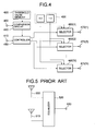
- this known system receives a plurality of signals from a plurality of antennas 500 and 510, equalizes and synthesizes these received signals in an equalizer 520, and then carries out their demodulation.
- reception performance against co-channel interference waves is improved.
- An object of the present invention is to offer an adaptive equalizer which minimises the above problems, while not complicating its configuration.
- Another object of the present invention is to offer an adaptive equalizer which minimises distortion by intersymbol interference and the deterioration of reception performance by co-channel interference waves, without using a diversity system.
- an equalizer which includes a channel impulse response vector calculator for estimating a channel impulse response vector h from received signals and calculating a channel impulse response vector h' by removing interference components from the estimated path impulse response vector h; and an equalizer for inputting the received signals and the channel impulse response vector h' , setting an internal parameter using the channel impulse response vector h' and then equalizing, based on the internal parameter, the received signals.
- the adaptive equalizer should include a maximum likelihood sequence estimator.
- the channel impulse response vector calculator should include means to input the received signals and the result of equalization of the received signals by the equalizer, to estimate the channel impulse response vector h using the equalization result and the received signals.
- the channel impulse response vector calculator should include a channel impulse response estimator for inputting the received signals and the equalization result and estimating a channel impulse response vector h , and a channel impulse response convertor for inputting the channel impulse response vector h and converting the channel impulse response vector h to the channel impulse response vector h' from which the interference components are removed.
- the channel impulse response estimator should include a transversal filter.
- the channel impulse response estimator should include a channel impulse response estimator circuit inputting the received signals and the equalization result and estimating the channel impulse response vector h; a training signal detector for detecting training signals from the input received signals; an equalization result output circuit for outputting the equalization result corresponding to the training signals; and switching means for inputting the equalization result from the equalization result output means and the equalization result of the received signals and outputting an equalization result from the equalization result output circuit to the channel impulse response estimation circuit when training signals have been detected based on a detection signal from the training signal detector, and means outputting an equalization result of the received signals to the channel impulse response estimation circuit when training signals have not been detected.
- the channel impulse response convertor means should include a plurality of absolute value operation means for inputting each component of the channel impulse response vector h , and calculating and outputting an absolute value of each component; a first maximum value detector for detecting and outputting a first maximum value among absolute values output from the plurality of absolute value operation means and specifying the absolute value operation means that has output the first maximum value; a gate for inputting absolute values output from the plurality of absolute value operation means and passing absolute values except for the first maximum value based on a specified signal from the first maximum value detector; a second maximum value detector for inputting the absolute values that have passed the gate, detecting a second maximum value among the absolute values that have passed the gate and outputting the second maximum value; a divider for inputting the first maximum value and the second maximum value and calculating the ratio between the first maximum value and the second maximum value; a weight controller for inputting the ratio calculated in the divider and the specified signal from the first maximum value detector and outputting a weight coefficient corresponding to each component of the channel impulse response vector
- the weight controller should include a weight coefficient memory for storing a plurality of weight coefficients; a selector for outputting only one weight coefficient among the plurality of weight coefficients; and a controller for inputting the specified signal from the first maximum value detector and the ratio output from the divider section and for outputting a control signal indicating a weight coefficient to be output to the selector.
- the weight controller should include a threshold value memory for storing a threshold value; a weight coefficient memory section for storing two weight coefficients; a selector for outputting a weight coefficient stored in the weight coefficient memory section; a comparison circuit for comparing the threshold value and the ratio output from the divider and for outputting a comparison signal; and a controller for inputting the comparison signal and the specified signal from the first maximum value detector and outputting a control signal indicating a weight coefficient to be output to the selector.
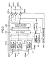
- Fig. 1 is a block diagram showing an embodiment of the present invention.
- 100 is an input terminal inputting reception signals
- 110 is an equalizer
- 120 is a channel impulse response vector calculator
- 130 is an output terminal outputting equalized reception signals.
- the equalizer 110 is configured by a maximum likelihood sequence estimator as shown, for example, in the paper "Digital Communications” Second Edition, 1989 by J.G.Proakis and in a U.S. Patent No. 5,127,025 "Space Diversity TDMA Receiver" by Mr. OKANOUE, one of the inventors of the present invention.
- reception signals input therein are equalized based on internal parameters. More, each internal parameter is set by each component of a channel impulse response vector h' described later on.
- the channel impulse response vector calculator 120 calculates a channel impulse response vector h' consisted of N components, from which all interference components are removed.
- This channel impulse response vector calculator 120 is configured by a channel impulse response estimator 121, a training signal detector 122, an training sequence generating circuit 123, switching circuit 124 and a channel impulse response convertor 125.
- the channel impulse response estimator 121 is configured by a transversal filter as shown, for example, Fig.6.7.5 in the paper "Digital Communications” Second Edition 1989, by J.G.Proakis.
- Training signal detector 122 is configured to output a detection signal by detecting training signals in reception signals.
- the training sequence generating circuit 123 which stores an equalization result of preset training signals, is configured to output the predetermind training sequence to the switching circuit 124.
- the switching circuit 124 inputs an predetermined training sequence from the training sequence generating circuit 123 and another equalization result of reception signals, and outputs one of them based on a detection signal from the training signal detector 122.
- an predetermined trainig sequence from the training sequence generating circuit 123 in case that the training signal detector 122 has detected a training signal or an equalization result of reception signals in case that the training signal detector 122 has not detected a training signal is input to the channel impulse response estimator 121 by selected in switching circuit 124.
- the channel impulse response estimator 121 estimates a channel impulse response h consisted of N components, then outputs it to the channel impulse response convertor 125.
- Fig.2 is a block diagram showing a configuration of the channel impulse response convertor 125.
- 200(1) to 200(N) are input terminals
- 210(1) to 210(N) are absolute value operation circuit
- 220 is a first maximum value detector
- 230 is a second maximum value detector
- 240 is a gate circuit
- 250 is a divider
- 260 is a weight controller
- 270(1) to 270(N) are multipliers
- 280(1) to 280(N) are output terminals.
- the channel impulse response convertor 125 removes interference components from a received channel impulse response h and converts this to a channel impulse response vector h' .
- This channel impulse response convertor 125 is configured by input terminals 200(1) to 200(N), absolute value operation circuits 210(1) to 210(N), a first maximum value detector 220, a second maximum value detector 230, a gate circuit 240, a divider 250, a weight controller 260 and multipliers 270(1) to 270(N).
- the input terminals 200(1) to 200(N) are configured to input each component of a channel impulse response h.
- the absolute value operation circuits 210(1) to 210(N) are configured to input each component of the channel impulse response h through the input terminals 200(1) to 200(N), calculate each absolute value of each component and output the results to the first maximum value detector 220 and the gate circuit 240.
- the first maximum value detector 220 is configured to detect the first maximum value (h max ) among N absolute values input therein and output it to the divider 250. More, it outputs a operation circuit specification signal specifying the absolute value operation section that have output the first maximum value to the gate circuit 240 and the weight controller 260.
- the gate circuit 240 is configured to gate only one absolute value that is the first maximum value (h max ) among absolute values of respective components input therein based on the operation circuit specification signal, and output (N-1) absolute values to the second maximum value detector 230.
- the maximum value detector 230 is configured to detect the largest value that is the second maximum value (h NEXT ) among (N-1) absolute values input therein, and output it to the divider 250.
- the divider 250 is configured to calculate a ratio of the first maximum value (h max ) and the second maximum value (h NEXT ) that is (h max /h NEXT ), and output the result to the weight controller 260.
- the weight controller 260 is configured to calculate each weight coefficient corresponding to each component of the channel impulse response h using the ratio (h max /h NEXT ) and the operation circuit specification signal, and output the results to the multipliers 270(1) to 270(N).
- the configuration of the weight controller 260 is explained later in detail.
- the multipliers 270(1) to 270(N) is configured to multiply each weight coefficient obtained in the weight controller 260 and each component of the channel impulse response h input through the input terminals 200(1) to 200(N), output the results to the output terminals 280(1) to 280(N).
- each component of the channel impulse response h is multiplied by each weight coefficient and interference components are removed, thus a channel impulse response vector h' is calculated. Then, the channel impulse response vector h' is input to the equalizer 110.
- the equalizer 110 sets up internal parameters based on the channel impulse response vector h' input therein , and equalizes reception signals using the internal parameters.
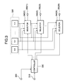
- Fig.3 is a block diagram of the weight controller 260.
- 300 and 310 are input terminals
- 320 is a weight coefficient memory
- 330 is a controller
- 340(1) to 340(N) are selectors
- 350(1) to 350(N) are output terminals.
- the input terminal 300 inputs the ratio (h max /h NEXT ) from the divider 250, the input terminal 310 inputs an operation circuit specification signal from the first maximum value detector 220.
- the weight coefficient memory 320 is configured to store a plurality of weight -coefficient and output these weight coefficients to the selectors 340(1) to 340(N).
- the controller 330 is configured to estimate interference components based on the ratio (h max /h NEXT ) input therein and output a control signal to the selectors 340(1) to 340(N) based on the operation circuit specification signal.
- the selectors 340(1) to 340(N) are configured to output, based on the control signal from the controller 330, only one weight coefficient among weight coefficients input therein.
- the controller 330 estimates magnitude of interference components based on the ratio (h max /h NEXT ) input therein. That is, it decides that interference components are small when the ratio (h max /h NEXT ) is large, or it decides that interference components are large when the ratio (h max /h NEXT ) is small. On the other hand, it specifies, based on the operation circuit specification signal, a selector to be input the first maximum value (h max ).
- the controller outputs a control signal that indicates the selector to output the maximum value among the weight coefficients input from the weight controller 330. Additionally, it outputs a control signal that indicates each selector to output the smaller value among the weight coefficients input from the weight controller 330 when the ratio (h max /h NEXT ) is large or the larger value among the weight coefficients input from the weight controller 330 when the ratio (h max /h NEXT ) is small.
- the respective weight coefficients corresponding to respective components of the channel impulse response h are output from the output terminals 350(1) to 350(N) and input to the multipliers 270(1) to 270 (N) .
- Fig.4 is a block diagram showing another embodiment of the weight controller 260.
- 400 and 410 are input terminals
- 420 is a threshold value memory
- 430 is a weight coefficient memory
- 440 is a comparison circuit
- 450 is a controller
- 460(1) to 460(N) are selectors
- 470(1) to 470(N) are output terminals.
- the input terminal 400 inputs the ratio (h max /h NEXT ) from the divider 250, the input terminal 410 inputs the operation circuit specification signal from the first maximum value detector 220.
- the threshold value memory 420 is configured to store a preset threshold value and output it to the comparison circuit 430.
- the weight coefficient memory 430 is configured to store 1 and 0 as weight coefficients, output them to the selectors 460(1) to 460(N).
- the comparison circuit 440 is configured to compare the threshold value and the ratio (h max /h NEXT ) input from the divider 250 through the input terminal 400, output the comparison result to the controller 450.
- the controller 450 is configured to output, based on the comparison result and the operation circuit specification signal from the first maximum value detector 220, a control signal to the selectors 460(1) to 460(N).
- the controller 450 compares a ratio (h max /h NEXT ) and a threshold value.
- the selectors 460(1) to 460(N) input the control signal, based on the control signal, outputs a weight coefficient corresponding to each component of the channel impulse response h to the output terminals 470(1) to 470(N).
- the weight coefficients output from the weight controller 260 configured as above are input to the multipliers 270(1) to 270(N).
Landscapes
- Engineering & Computer Science (AREA)
- Quality & Reliability (AREA)
- Computer Networks & Wireless Communication (AREA)
- Signal Processing (AREA)
- Cable Transmission Systems, Equalization Of Radio And Reduction Of Echo (AREA)
- Filters That Use Time-Delay Elements (AREA)
- Noise Elimination (AREA)
Applications Claiming Priority (3)
| Application Number | Priority Date | Filing Date | Title |
|---|---|---|---|
| JP347220/92 | 1992-12-25 | ||
| JP34722092 | 1992-12-25 | ||
| JP4347220A JP2605566B2 (ja) | 1992-12-25 | 1992-12-25 | 適応型等化器 |
Publications (3)
| Publication Number | Publication Date |
|---|---|
| EP0604208A2 true EP0604208A2 (fr) | 1994-06-29 |
| EP0604208A3 EP0604208A3 (fr) | 1995-01-18 |
| EP0604208B1 EP0604208B1 (fr) | 2000-04-19 |
Family
ID=18388740
Family Applications (1)
| Application Number | Title | Priority Date | Filing Date |
|---|---|---|---|
| EP93310408A Expired - Lifetime EP0604208B1 (fr) | 1992-12-25 | 1993-12-22 | Equilibreur adaptatif |
Country Status (5)
| Country | Link |
|---|---|
| US (1) | US5519727A (fr) |
| EP (1) | EP0604208B1 (fr) |
| JP (1) | JP2605566B2 (fr) |
| CA (1) | CA2112020C (fr) |
| DE (1) | DE69328413T2 (fr) |
Cited By (7)
| Publication number | Priority date | Publication date | Assignee | Title |
|---|---|---|---|---|
| WO1996008881A3 (fr) * | 1994-09-12 | 1996-06-06 | Nokia Telecommunications Oy | Procede de reception et recepteur |
| WO1996011533A3 (fr) * | 1994-10-07 | 1996-06-13 | Nokia Telecommunications Oy | Detection de signaux dans un systeme tdma |
| GB2287620B (en) * | 1994-03-10 | 1998-12-16 | Roke Manor Research | A digital cellular mobile radio receiver |
| WO2000054427A1 (fr) * | 1999-03-10 | 2000-09-14 | Nokia Mobile Phones Ltd. | Egaliseur de canaux adaptatif |
| WO2001022571A1 (fr) * | 1999-09-17 | 2001-03-29 | Telefonaktiebolaget Lm Ericsson (Publ) | Appareil et procede permettant de supprimer sensiblement un signal brouilleur a modulation d'amplitude de voie proche |
| US6256486B1 (en) | 1999-09-09 | 2001-07-03 | Nortel Networks Limited | Method and apparatus for measuring co-channel interference |
| GB2388503A (en) * | 2002-04-29 | 2003-11-12 | Thales Plc | Channel estimation |
Families Citing this family (27)
| Publication number | Priority date | Publication date | Assignee | Title |
|---|---|---|---|---|
| FR2708162B1 (fr) * | 1993-07-20 | 1995-09-01 | Alcatel Mobile Comm France | Procédé pour déterminer la longueur optimale d'un bloc de données dans un système de communication à accès multiple à répartition dans le temps (AMRT). |
| JP2571008B2 (ja) * | 1993-12-24 | 1997-01-16 | 日本電気株式会社 | 適応型最尤系列推定器 |
| US5805638A (en) * | 1995-12-04 | 1998-09-08 | Lucent Technologies Inc. | Systems and methods of digital wireless communication using equalization |
| DE19614543C1 (de) * | 1996-04-12 | 1997-08-28 | Philips Patentverwaltung | Entzerrer mit erweiterter Kanalschätzung für einen Empfänger in einem digitalen Übertragungssystem |
| FI103539B1 (fi) * | 1996-07-03 | 1999-07-15 | Nokia Telecommunications Oy | Menetelmä samankanavasignaalien voimakkuuden määrittämiseksi ja vastaanotin |
| FI101845B1 (fi) * | 1996-08-09 | 1998-08-31 | Nokia Telecommunications Oy | Menetelmä yhteyden laadun määrittämiseksi sekä vastaanotin |
| KR100241890B1 (ko) | 1997-01-10 | 2000-03-02 | 윤종용 | 디지털 통신 시스템에서 간섭 제거 회로 |
| US5933768A (en) * | 1997-02-28 | 1999-08-03 | Telefonaktiebolaget L/M Ericsson | Receiver apparatus, and associated method, for receiving a receive signal transmitted upon a channel susceptible to interference |
| US6047024A (en) * | 1997-08-22 | 2000-04-04 | Alcatel Internetworking, Inc. | Device for equalizing channel-distorted signals |
| US6704317B1 (en) | 1998-05-27 | 2004-03-09 | 3Com Corporation | Multi-carrier LAN modem server |
| US6891887B1 (en) | 1998-05-27 | 2005-05-10 | 3Com Corporation | Multi-carrier LAN adapter device using interpolative equalizer |
| US6507585B1 (en) | 1998-05-27 | 2003-01-14 | 3Com Corporation | Multi-carrier LAN adapter device using frequency domain equalizer |
| US6377683B1 (en) | 1998-05-29 | 2002-04-23 | 3Com Corporation | Low complexity frequency domain echo canceller for DMT transceivers |
| US6603811B1 (en) | 1998-05-29 | 2003-08-05 | 3Com Corporation | Low complexity frequency domain equalizer having fast re-lock |
| AT407933B (de) * | 1998-06-09 | 2001-07-25 | Juha Dipl Ing Laurila | Verfahren zur trennung und zur detektion von gleichkanal-signalen |
| EP1147623B1 (fr) * | 1998-11-18 | 2003-07-02 | Nokia Corporation | Procede pour modifier la reponse impulsionnelle de canal dans des systemes amrt |
| KR100299767B1 (ko) * | 1999-04-20 | 2001-10-29 | 김춘호 | 채널 단축 등화기 |
| US6751202B1 (en) | 1999-04-30 | 2004-06-15 | 3Com Corporation | Filtered transmit cancellation in a full-duplex modem data access arrangement (DAA) |
| US6643271B1 (en) | 1999-04-30 | 2003-11-04 | 3Com Corporation | Adjustable gain transmit cancellation in a full-duplex modem data access arrangement (DAA) |
| US6912250B1 (en) * | 1999-11-12 | 2005-06-28 | Cornell Research Foundation Inc. | System and methods for precursor cancellation of intersymbol interference in a receiver |
| EP1117219B1 (fr) * | 2000-01-11 | 2005-09-07 | Lucent Technologies Inc. | Correction de décalage de fréquence en présence d'interférence intersymbole |
| US6782043B1 (en) * | 2000-01-18 | 2004-08-24 | Lsi Logic Corporation | Method and apparatus for estimating the length of a transmission line |
| KR20030005700A (ko) * | 2001-07-10 | 2003-01-23 | 한기열 | 채널등화 전처리 시스템 |
| US7194025B2 (en) * | 2003-06-16 | 2007-03-20 | Harris Corporation | Updating adaptive equalizer coefficients using known or predictable bit patterns distributed among unknown data |
| US7440497B2 (en) * | 2004-11-01 | 2008-10-21 | Lsi Corporation | Serial data link using decision feedback equalization |
| KR20130049978A (ko) * | 2011-11-07 | 2013-05-15 | 한국전자통신연구원 | 채널 추정 장치 및 방법 |
| TWI773966B (zh) * | 2020-02-20 | 2022-08-11 | 瑞昱半導體股份有限公司 | 運作方法以及接收裝置 |
Family Cites Families (16)
| Publication number | Priority date | Publication date | Assignee | Title |
|---|---|---|---|---|
| FR2482809B1 (fr) * | 1980-05-14 | 1986-11-14 | Labo Electronique Physique | Systeme adaptatif de reception de donnees numeriques a compensation des distorsions d'amplitude et de phase introduites par le canal de transmission des donnees |
| US4430743A (en) * | 1980-11-17 | 1984-02-07 | Nippon Electric Co., Ltd. | Fast start-up system for transversal equalizers |
| DE69024525T2 (de) * | 1989-05-02 | 1996-05-15 | Nippon Electric Co | TDMA-Raumdiversity-Empfänger |
| US5020078A (en) * | 1989-08-11 | 1991-05-28 | Bell Communications Research, Inc. | Baudrate timing recovery technique |
| JP2508298B2 (ja) * | 1989-10-18 | 1996-06-19 | 日本電気株式会社 | ディジタル信号受信方式及び受信装置 |
| JP2795935B2 (ja) * | 1989-11-24 | 1998-09-10 | 三菱電機株式会社 | 最尤系列推定装置 |
| JPH03195129A (ja) * | 1989-12-22 | 1991-08-26 | Mitsubishi Electric Corp | 最尤系列推定装置 |
| JP3060480B2 (ja) * | 1990-03-28 | 2000-07-10 | 松下電器産業株式会社 | データ受信装置 |
| JP2560896B2 (ja) * | 1990-07-31 | 1996-12-04 | 日本電気株式会社 | 最尤受信器 |
| GB2247812B (en) * | 1990-09-06 | 1994-08-31 | Motorola Inc | Equalizer for linear modulated signal |
| DE4135495A1 (de) * | 1990-11-02 | 1992-05-07 | Telefunken Systemtechnik | Verfahren zur entzerrung digitaler nachrichtensignale sowie entzerrer zum durchfuehren des verfahrens |
| DE4039245A1 (de) * | 1990-12-08 | 1992-06-11 | Philips Patentverwaltung | Empfaenger mit mindestens zwei empfangszweigen |
| US5251233A (en) * | 1990-12-20 | 1993-10-05 | Motorola, Inc. | Apparatus and method for equalizing a corrupted signal in a receiver |
| US5231648A (en) * | 1991-03-21 | 1993-07-27 | Northern Telecom Limited | Adaptive equalizer for digital cellular radio |
| JP2621685B2 (ja) * | 1991-05-29 | 1997-06-18 | 日本電気株式会社 | 適応型最尤系列推定装置 |
| FR2679721B1 (fr) * | 1991-07-22 | 1993-09-24 | Alcatel Radiotelephone | Procede d'egalisation adaptative reduisant l'interference intersymbole, et dispositif de reception et application correspondants. |
-
1992
- 1992-12-25 JP JP4347220A patent/JP2605566B2/ja not_active Expired - Lifetime
-
1993
- 1993-12-21 CA CA002112020A patent/CA2112020C/fr not_active Expired - Fee Related
- 1993-12-21 US US08/171,093 patent/US5519727A/en not_active Expired - Fee Related
- 1993-12-22 EP EP93310408A patent/EP0604208B1/fr not_active Expired - Lifetime
- 1993-12-22 DE DE69328413T patent/DE69328413T2/de not_active Expired - Fee Related
Cited By (13)
| Publication number | Priority date | Publication date | Assignee | Title |
|---|---|---|---|---|
| GB2287620B (en) * | 1994-03-10 | 1998-12-16 | Roke Manor Research | A digital cellular mobile radio receiver |
| CN1086074C (zh) * | 1994-09-12 | 2002-06-05 | 诺基亚电信公司 | 一种接收方法以及一种接收机 |
| US5930289A (en) * | 1994-09-12 | 1999-07-27 | Nokia Telecommunications Oy | CDMA reception method and a CDMA receiver which calculates an estimate from samples for each desired signal during a monitoring period |
| WO1996008881A3 (fr) * | 1994-09-12 | 1996-06-06 | Nokia Telecommunications Oy | Procede de reception et recepteur |
| WO1996011533A3 (fr) * | 1994-10-07 | 1996-06-13 | Nokia Telecommunications Oy | Detection de signaux dans un systeme tdma |
| US5995499A (en) * | 1994-10-07 | 1999-11-30 | Nokia Telecommunications Oy | Signal detection in a TDMA system |
| WO2000054427A1 (fr) * | 1999-03-10 | 2000-09-14 | Nokia Mobile Phones Ltd. | Egaliseur de canaux adaptatif |
| WO2001018978A3 (fr) * | 1999-09-09 | 2002-06-06 | Nortel Networks Ltd | Procede et dispositif de mesure d'interference dans le meme canal |
| US6256486B1 (en) | 1999-09-09 | 2001-07-03 | Nortel Networks Limited | Method and apparatus for measuring co-channel interference |
| WO2001022571A1 (fr) * | 1999-09-17 | 2001-03-29 | Telefonaktiebolaget Lm Ericsson (Publ) | Appareil et procede permettant de supprimer sensiblement un signal brouilleur a modulation d'amplitude de voie proche |
| US6934346B2 (en) | 1999-09-17 | 2005-08-23 | Telefonaktiebolaget L M Ericsson (Publ) | Apparatus and method for substantially eliminating a near-channel interfering amplitude modulated signal |
| GB2388503A (en) * | 2002-04-29 | 2003-11-12 | Thales Plc | Channel estimation |
| GB2388503B (en) * | 2002-04-29 | 2005-11-30 | Thales Plc | Channel estimation |
Also Published As
| Publication number | Publication date |
|---|---|
| US5519727A (en) | 1996-05-21 |
| DE69328413D1 (de) | 2000-05-25 |
| EP0604208A3 (fr) | 1995-01-18 |
| DE69328413T2 (de) | 2000-12-21 |
| JP2605566B2 (ja) | 1997-04-30 |
| EP0604208B1 (fr) | 2000-04-19 |
| CA2112020C (fr) | 1997-12-09 |
| JPH06197032A (ja) | 1994-07-15 |
| CA2112020A1 (fr) | 1994-06-26 |
Similar Documents
| Publication | Publication Date | Title |
|---|---|---|
| US5519727A (en) | Adaptive equalizer | |
| CA2084034C (fr) | Recepteur adaptatif | |
| US5164961A (en) | Method and apparatus for adapting a viterbi algorithm to a channel having varying transmission properties | |
| EP0755141B1 (fr) | Egalisation adaptative, à décision récursive, pour systèmes de communication | |
| US6246732B1 (en) | Demodulator including adaptive equalizer and demodulating method in digital communications | |
| JP2556179B2 (ja) | ダイバーシティ受信方式 | |
| KR100447201B1 (ko) | 채널 등화 장치 및 이를 이용한 디지털 tv 수신기 | |
| US6347126B1 (en) | Receiver with a frequency offset correcting function | |
| EP0942561B1 (fr) | Pas adaptatif pour estimation de canal | |
| EP0449327B1 (fr) | Récepteur à diversité d'espace et à immunité contre le bruit | |
| EP0544315B1 (fr) | Appareil d'estimation de séquence à vraisemblance maximale | |
| US5297171A (en) | Receiver comprising at least two receive branches | |
| US6952570B2 (en) | Wireless communication receiver that determines frequency offset | |
| EP0577901B1 (fr) | Procédé et dispositif d'égalisation adaptative | |
| EP0453814B1 (fr) | Système adaptatif d'estimation de réponses impulsionnelles de canal au moyen d'estimation de séquence ayant un maximum de vraisemblance | |
| JP3145295B2 (ja) | データ受信装置 | |
| US5359628A (en) | Channel impulse response estimator for use in an adaptive maximum likelihood sequence estimation receiver which is applicable to a communication system having a channel characteristic with rapid fluctuation | |
| KR0134340B1 (ko) | 블라인드 등화시스템의 알고리즘제어방법 | |
| EP3997795B1 (fr) | Égaliseur à saut adaptatif | |
| US6349112B1 (en) | Adaptive equalizer compensating signal distortion on transmission path | |
| JP3138586B2 (ja) | 適応等化器および適応ダイバーシチ等化器 | |
| US6292510B1 (en) | Automatic equalization method and automatic equalizer | |
| EP1128617B1 (fr) | Procédé et récepteur mettant en oeuvre une estimation de voie pour égaliser des signaux numériques | |
| US6366612B1 (en) | Automatic equalizer | |
| JPH0795715B2 (ja) | 等化器 |
Legal Events
| Date | Code | Title | Description |
|---|---|---|---|
| PUAI | Public reference made under article 153(3) epc to a published international application that has entered the european phase |
Free format text: ORIGINAL CODE: 0009012 |
|
| AK | Designated contracting states |
Kind code of ref document: A2 Designated state(s): DE GB NL SE |
|
| PUAL | Search report despatched |
Free format text: ORIGINAL CODE: 0009013 |
|
| RHK1 | Main classification (correction) |
Ipc: H04B 7/08 |
|
| AK | Designated contracting states |
Kind code of ref document: A3 Designated state(s): DE GB NL SE |
|
| 17P | Request for examination filed |
Effective date: 19941212 |
|
| 17Q | First examination report despatched |
Effective date: 19980831 |
|
| GRAG | Despatch of communication of intention to grant |
Free format text: ORIGINAL CODE: EPIDOS AGRA |
|
| GRAG | Despatch of communication of intention to grant |
Free format text: ORIGINAL CODE: EPIDOS AGRA |
|
| GRAH | Despatch of communication of intention to grant a patent |
Free format text: ORIGINAL CODE: EPIDOS IGRA |
|
| GRAH | Despatch of communication of intention to grant a patent |
Free format text: ORIGINAL CODE: EPIDOS IGRA |
|
| GRAA | (expected) grant |
Free format text: ORIGINAL CODE: 0009210 |
|
| AK | Designated contracting states |
Kind code of ref document: B1 Designated state(s): DE GB NL SE |
|
| REF | Corresponds to: |
Ref document number: 69328413 Country of ref document: DE Date of ref document: 20000525 |
|
| EN | Fr: translation not filed | ||
| PLBE | No opposition filed within time limit |
Free format text: ORIGINAL CODE: 0009261 |
|
| STAA | Information on the status of an ep patent application or granted ep patent |
Free format text: STATUS: NO OPPOSITION FILED WITHIN TIME LIMIT |
|
| 26N | No opposition filed | ||
| REG | Reference to a national code |
Ref country code: GB Ref legal event code: IF02 |
|
| PGFP | Annual fee paid to national office [announced via postgrant information from national office to epo] |
Ref country code: SE Payment date: 20021203 Year of fee payment: 10 |
|
| PGFP | Annual fee paid to national office [announced via postgrant information from national office to epo] |
Ref country code: GB Payment date: 20021218 Year of fee payment: 10 |
|
| PGFP | Annual fee paid to national office [announced via postgrant information from national office to epo] |
Ref country code: NL Payment date: 20021227 Year of fee payment: 10 |
|
| PGFP | Annual fee paid to national office [announced via postgrant information from national office to epo] |
Ref country code: DE Payment date: 20021231 Year of fee payment: 10 |
|
| PG25 | Lapsed in a contracting state [announced via postgrant information from national office to epo] |
Ref country code: GB Free format text: LAPSE BECAUSE OF NON-PAYMENT OF DUE FEES Effective date: 20031222 |
|
| PG25 | Lapsed in a contracting state [announced via postgrant information from national office to epo] |
Ref country code: SE Free format text: LAPSE BECAUSE OF NON-PAYMENT OF DUE FEES Effective date: 20031223 |
|
| PG25 | Lapsed in a contracting state [announced via postgrant information from national office to epo] |
Ref country code: NL Free format text: LAPSE BECAUSE OF NON-PAYMENT OF DUE FEES Effective date: 20040701 Ref country code: DE Free format text: LAPSE BECAUSE OF NON-PAYMENT OF DUE FEES Effective date: 20040701 |
|
| EUG | Se: european patent has lapsed | ||
| GBPC | Gb: european patent ceased through non-payment of renewal fee |
Effective date: 20031222 |
|
| NLV4 | Nl: lapsed or anulled due to non-payment of the annual fee |
Effective date: 20040701 |