EP0604233A2 - Verfahren und Vorrichtung zur Messung der Hochfrequenz-C-V-Charakteristik einer MIS-Anordnung - Google Patents
Verfahren und Vorrichtung zur Messung der Hochfrequenz-C-V-Charakteristik einer MIS-Anordnung Download PDFInfo
- Publication number
- EP0604233A2 EP0604233A2 EP93310503A EP93310503A EP0604233A2 EP 0604233 A2 EP0604233 A2 EP 0604233A2 EP 93310503 A EP93310503 A EP 93310503A EP 93310503 A EP93310503 A EP 93310503A EP 0604233 A2 EP0604233 A2 EP 0604233A2
- Authority
- EP
- European Patent Office
- Prior art keywords
- mis
- voltage
- frequency
- light
- shielding
- Prior art date
- Legal status (The legal status is an assumption and is not a legal conclusion. Google has not performed a legal analysis and makes no representation as to the accuracy of the status listed.)
- Ceased
Links
Images


Classifications
-
- G—PHYSICS
- G01—MEASURING; TESTING
- G01R—MEASURING ELECTRIC VARIABLES; MEASURING MAGNETIC VARIABLES
- G01R31/00—Arrangements for testing electric properties; Arrangements for locating electric faults; Arrangements for electrical testing characterised by what is being tested not provided for elsewhere
- G01R31/26—Testing of individual semiconductor devices
- G01R31/2601—Apparatus or methods therefor
- G01R31/2603—Apparatus or methods therefor for curve tracing of semiconductor characteristics, e.g. on oscilloscope
Definitions
- the present invention relates to a method and an apparatus for measuring the high-frequency C-V characteristics of a metal-insulator-semiconductor (MIS) device and more particularly to a method and an apparatus for measuring that of a metal-oxide-semiconductor (MOS) device.
- MIS metal-insulator-semiconductor
- MOS metal-oxide-semiconductor
- a high-frequency C-V characteristics is conventionally measured for the relation between the gate voltage and series connected capacitance (hereinafter referred to as MOS capacitance) of a gate oxide and the depletion layer near the semiconductor surface.
- a voltage response of the MOS capacitance is measured when a voltage is applied to a gate electrode of the MOS device and the sweep direction of the applied voltage is turned from the accumulation to the inversion or vice versa. For example, when the voltage response of the MOS capacitance is measured so that the MOS device is exposed to light from incandescent lamp or fluorescent lamp, it is incorrectly measured.
- FIG.6 shows an actual high-frequency C-V characteristics of the MOS capacitor in solid line when the surface of the MOS capacitor is exposed to light from fluorescent lamp and a theoretical high-frequency C-V characteristics of the MOS capacitor in dotted line (see THE BELL SYSTEM TECHNICAL JOURNAL, September 1966, pp.1097-1122).
- the MOS capacitance should be in equilibrium but actually increases, so that the actual curve is out of accordance with the theoretical curve. This is because that a light energy from fluorescent lamp induces excess minority carriers at the semiconductor surface.
- the MOS capacitance cannot be accurately measured under a condition of exposing the MOS capacitor to light from fluorescent or incandescent lamp.
- a prior-art apparatus for measuring the high-frequency C-V characteristics measures the high-frequency C-V characteristics in a shading and radiation-shielding box i.e. shielding-box.
- the measurement of the high-frequency C-V characteristics in the shielding-box has a drawback described below.
- FIG.7 shows in solid line an actual high-frequency C-V characteristics measured using the shielding box and a theoretical high-frequency C-V characteristics in dotted line.
- the MOS capacitance should be in equilibrium, i.e., constant. However, it actually decreases the inversion region and is entirely out of accordance with the theoretical curve, as shown in FIG.7. Since the generation of minority carriers scarcely follow the sweep speed of the applied voltage, the depletion layer width increases with the applied voltage so that the equilibrium is not arrived. Therefore, the prior-art apparatus of measuring the high-frequency C-V characteristics cannot measure an exact MOS capacitance.
- the sweep speed of the gate voltage must be reduced in order to obtain a sufficient energy to induce the minority carriers at the semiconductor surface.
- a measuring time required up to the equilibrium is at most 1 hr per measurement point, so that the measurement efficiency is greatly reduced.
- a method of measuring the high-frequency C-V characteristics of a MIS device comprises the steps of: illuminating the MIS device by means of an illuminant emitting a light of a pre-determined wavelength which prevents excess carriers from being generated at a surface of the semi-conductor of the MIS device; applying a voltage of a high frequency to a gate electrode of the MIS device; and measuring the MIS capacitance of the MIS device receiving said voltage.
- the MIS device is placed in a shielding-box to shield the MIS device from outside electro-magnetic radiation.
- an apparatus for measuring the high-frequency C-V characteristics of a MIS device comprises: a shielding-box shielding the MIS device from outside electro-magnetic radiation; an illuminant provided within said shielding-box and emitting a light of a pre-determined wavelength preventing induction of excess carriers at a surface of the semiconductor of the MIS device; means for applying a voltage of a high frequency to a gate electrode of the MIS device; and means for measuring the MIS capacitance of the MIS device receiving said voltage.
- An advantage of the present invention is that the method and apparatus for measuring the high frequency C-V characteristics of a device promotes the induction of minority carriers in the semi-conductor and quickly produces the inversion layer and stably maintains the equilibrium of the inversion layer so as to accurately measure the capacitance in response to a voltage applied to a gate electrode of the device.
- the MIS device may be a MOS device.
- the device may be a MOS capacitor and the shielding box have a top wall and a bottom wall, and the apparatus also include a C-V meter which applies a voltage of a high frequency to the gate electrode of the MOS capacitor and changes a sweep direction of said voltage of a sweep width, said C-V meter picking up a vector voltage produced across and a vector current passing through the MOS capacitor to measure the MOS capacitance of the MOS capacitor.
- the pre-determined wavelength is at least 500 nm in the case where the device is derived from a silicon wafer, or where the pre-determined wavelength is at least 1200 nm in the case where the device is derived from a germanium wafer, or where the pre-determined wavelength is at least 800 nm in the case where the device is derived from a gallium-arsenide wafer or where the predetermined wavelength is at least 850 nm in the case where the device is derived from an indium-phosphide wafer.
- the illuminant may comprise a light source and a filter passing a component of a pre-determined or effective wavelength of a light from the light source.
- the wavelength of the light illuminating the surface of the silicon device is less than 500 nm, excess minority carriers are generated only near the silicon surface since the absorption co-efficient of the silicon substrate is great in respect of the light of that wavelength so that the energy of the light of that wavelength generates hole-electron pairs.
- the energy gap E g of the silicon semi-conductor is 1.12 eV, the silicon substrate does not absorb a light of more than 1100 nm wavelength and almost no minority carriers are induced.
- the present invention restricts the wavelength of the light to 500 nm to 1100 nm in respect of the device fabricated or derived from the silicon wafer.
- the light in a range of wavelengths which prevents the induction of the excess carriers at the semi-conductor surface illuminates the surface of the device, the light energy is introduced into a certain depth in the semi-conductor to promote the generation of hole-electron pairs and further internal minority carries.
- the magnitude of the applied voltage is gradually increased, so that an electric field produced by the gate voltage easily induces the minority carriers to the semi-conductor surface.
- the generation and the movement of the minority carriers quickly follow the high sweep speed of the voltage applied to the electrode gate, so that a measuring time of the high-frequency C-V characteristics is reduced.
- the present invention quickly and accurately measures the capacitance of the device.
- the physical characteristic values such as the carrier concentration N sub in the semi-conductor substrate, the flat band voltage V fb required for flattening the energy band at the surface of the semiconductor substrate, the threshold voltage V th , and the charge density Q ss in the interface between the insulator and the semi-conductor can accurately be obtained from the measurement results of the capacitance.
- the wavelength of the light from the illuminant is at least 500 nm
- an energy exceeding the band gap energy of the silicon device is introduced into a certain depth in the silicon semi-conductor to promote the generation of hole-electron pairs and further internal minority carriers.
- FIG.1 a silicon semiconductor wafer is indicated at 2.
- the wafer 2 is a sample of which the MOS capacitance is to be measured.
- the wafer 2 has a MOS capacitor as a MOS device fabricated thereon.
- the MOS capacitor comprises, e.g., a p-type silicon substrate 11, an oxide film 12 grown on the top surface of the substrate 11, and gate electrodes 13 of polysilicon or aluminum deposited on a portion of the oxide film 12.
- a high-frequency C-V characteristics measuring apparatus 1 comprises a shading and radiation sielding box i.e. shielding-box 3, a wafer stage 4 on which the wafer 2 is placed, a stage support 5 fixed to the bottom of the shielding-box 3, an illuminant 6 right above the wafer stage 4 and fixed to the ceiling of the shielding-box 3, and a capacitance versus voltage (C-V) meter 7 provided outside the shielding-box 3 and having two lead cables 7a and 7b the front ends of which have probes.
- a shading and radiation sielding box i.e. shielding-box 3
- a wafer stage 4 on which the wafer 2 is placed
- a stage support 5 fixed to the bottom of the shielding-box 3
- an illuminant 6 right above the wafer stage 4 and fixed to the ceiling of the shielding-box 3
- C-V capacitance versus voltage
- the shielding-box 3 is made of stainless steel. However, a material for the shielding-box 3 is not restricted.
- the shielding box 3 intercepts natural light, light form incandescent and fluorescent lamps, etc.
- the stage support 5 contains a vacuum chuck sucking the wafer 2 to fasten it to the wafer stage 4.
- the illuminant 6 emits a light of 500 nm to 700 nm wavelength, preferably, 500 nm to 700 nm wavelength, i.e., yellow light, to the top surface of the wafer 2 with a uniform illuminance.
- the illuminant 6 may emit a light of at least 500 nm wavelength.
- a controller controls the illuminant 6 to automatically illuminate the top surface of the wafer 2.
- the illuminant 6 may be manually controlled.
- a lamp 9 of a microscope 8 employed for confirming an attachment of one probe from the lead cable 7a to a gate electrode 13 may be employed in place of the illuminant 6.
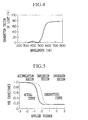
- the illuminant 6 and the lamp 9 of the microscope 8 may comprise an incandescent lamp (not shown) and a wavelength selection filter (not shown) cutting off a light of less than 500 nm wavelength and passing a light of a 600 nm or more wavelength at 60 % or more transmission factor of light, as shown in FIG.4.
- the C-V meter 7 measures the MOS capacitance between the gate electrode 13 and the underside or backside of the substrate 11.
- the probe at the front end of the lead 7a is connected with the gate electrode 13 and the probe at the front end of the lead 7b is connected with the backside of the substrate 11.
- the C-V meter 7 is designed to apply a pulse voltage of, e.g., 1-MHz frequency and, e.g., a 3-V sweep width as a measuring signal to the gate electrode 13 and pick up a vector voltage produced across and a vector current passing through the MOS capacitor to measure the MOS capacitance.
- the wafer 2 is placed on the wafer stage 4 and the probes of the C-V meter 7 are connected with the gate electrode 13 and the backside of the wafer 2.
- the illuminant 6 emits the light of 500 nm to 700 nm wavelength and the C-V meter 7 outputs a predetermined pulse voltage and detects a resulting vector voltage and a resulting vector current.
- FIG.5 shows a theoretical high-frequency C-V curve in dotted line and an actual high-frequency C-V curve in solid line.
- the applied voltage to the gate electrode 13 is gradually increased from the accumulation to the inversion and successively vice versa.
- FIG.5 shows the actual high-frequency C-V curve in good accordance with the theoretical high-frequency C-V curve except the range corresponding the depletion layer. This indicates that the measurement of the high-frequency C-V characteristics of the MOS capacitor is accurately carried out.
- the actual high-frequency C-V curve is in good accordance with the theoretical high-frequency C-V curve. This indicates that an optimum number of minority carriers induced by the light from the illuminant 6 for the formation of the inversion layer at the surface of the substrate 11 quickly follow the sweep speed of the applied voltage to the gate electrode 13 and the induction of excess minority carriers at the surface of the substrate 11 are prevented so that the equilibrium of the inversion layer is maintained.
- a translational difference between the actual and theoretical high-frequency C-V characteristics curves in the range corresponding to the depletion layer is due to an oxide charge and a work function difference between the gate electrode 13 and the wafer 2 (see J. Electrochem. Soc.: SOLID STATE SCIENCE, Vol.114, No.3, March 1967, pp.266-273).
- the present invention is not restricted to the above embodiment.
- the high-frequency C-V characteristics of the MOS device may alternatively be measured in a highly-shading measuring room instead of in the shielding-box 3 using a light of 500 nm to 700 nm wavelength.
- an illuminant may comprise an incandescent lamp and a wavelength selection filter passing the light of at least 500 nm wavelength.
- the embodiment has described the case in which the silicon substrate is employed as the semiconductor substrate 11 and the light of 500 nm or more wavelength is employed.
- the present invention employs a light of 1200 nm or more wavelength in measuring the high-frequency C-V characteristics of a germanium MOS device, a light of 800 nm or more wavelength in measuring that of a gallium-arsenide MOS device, and a light of 850 nm or more wavelength in measuring that of an indium phosphide MOS device.
Landscapes
- Physics & Mathematics (AREA)
- General Physics & Mathematics (AREA)
- Testing Or Measuring Of Semiconductors Or The Like (AREA)
Applications Claiming Priority (2)
| Application Number | Priority Date | Filing Date | Title |
|---|---|---|---|
| JP35758692 | 1992-12-24 | ||
| JP357586/92 | 1992-12-24 |
Publications (2)
| Publication Number | Publication Date |
|---|---|
| EP0604233A2 true EP0604233A2 (de) | 1994-06-29 |
| EP0604233A3 EP0604233A3 (de) | 1995-05-24 |
Family
ID=18454885
Family Applications (1)
| Application Number | Title | Priority Date | Filing Date |
|---|---|---|---|
| EP93310503A Ceased EP0604233A3 (de) | 1992-12-24 | 1993-12-23 | Verfahren und Vorrichtung zur Messung der Hochfrequenz-C-V-Charakteristik einer MIS-Anordnung. |
Country Status (2)
| Country | Link |
|---|---|
| US (1) | US5442302A (de) |
| EP (1) | EP0604233A3 (de) |
Cited By (1)
| Publication number | Priority date | Publication date | Assignee | Title |
|---|---|---|---|---|
| US5475319A (en) * | 1993-06-08 | 1995-12-12 | Dainippon Screen Mfg. Co., Ltd. | Method of measuring electric charge of semiconductor wafer |
Families Citing this family (6)
| Publication number | Priority date | Publication date | Assignee | Title |
|---|---|---|---|---|
| JP3274924B2 (ja) * | 1993-12-15 | 2002-04-15 | 株式会社東芝 | 半導体装置のスクリーニング方法 |
| WO1998045719A1 (en) | 1997-04-04 | 1998-10-15 | University Of Florida | Method for testing and diagnosing mos transistors |
| DE19740025A1 (de) * | 1997-09-11 | 1999-03-25 | Wacker Siltronic Halbleitermat | Dotierstoff-Messung |
| KR100707585B1 (ko) * | 2005-12-29 | 2007-04-13 | 동부일렉트로닉스 주식회사 | Mos 트랜지스터 소자의 정전용량-전압 특성을 이용한캐리어 농도 분포 측정 자동화 시스템 및 방법 |
| US7548067B2 (en) * | 2006-10-25 | 2009-06-16 | Sematech, Inc. | Methods for measuring capacitance |
| WO2012021595A1 (en) * | 2010-08-13 | 2012-02-16 | First Solar, Inc | In-process measurement apparatus |
Family Cites Families (4)
| Publication number | Priority date | Publication date | Assignee | Title |
|---|---|---|---|---|
| US4323842A (en) * | 1980-02-19 | 1982-04-06 | The United States Of America As Represented By The Secretary Of The Army | Method and apparatus for electrically testing radiation susceptibility of MOS gate devices |
| JP2690908B2 (ja) * | 1987-09-25 | 1997-12-17 | 株式会社日立製作所 | 表面計測装置 |
| JPH07117570B2 (ja) * | 1988-09-12 | 1995-12-18 | 日産自動車株式会社 | 半導体のc−v計測装置 |
| DE3917702A1 (de) * | 1989-05-31 | 1990-12-06 | Siemens Ag | Verfahren zur ortsaufgeloesten bestimmung der diffusionslaenge von minoritaetsladungstraegern in einem halbleiterkristallkoerper mit hilfe einer elektrolytischen zelle |
-
1993
- 1993-12-22 US US08/171,406 patent/US5442302A/en not_active Expired - Fee Related
- 1993-12-23 EP EP93310503A patent/EP0604233A3/de not_active Ceased
Cited By (1)
| Publication number | Priority date | Publication date | Assignee | Title |
|---|---|---|---|---|
| US5475319A (en) * | 1993-06-08 | 1995-12-12 | Dainippon Screen Mfg. Co., Ltd. | Method of measuring electric charge of semiconductor wafer |
Also Published As
| Publication number | Publication date |
|---|---|
| EP0604233A3 (de) | 1995-05-24 |
| US5442302A (en) | 1995-08-15 |
Similar Documents
| Publication | Publication Date | Title |
|---|---|---|
| US8896338B2 (en) | Electrical characterization of semiconductor materials | |
| US7898280B2 (en) | Electrical characterization of semiconductor materials | |
| US5049816A (en) | Semiconductor substrate minority carrier lifetime measurements | |
| US5907764A (en) | In-line detection and assessment of net charge in PECVD silicon dioxide (oxide) layers | |
| US4286215A (en) | Method and apparatus for the contactless monitoring carrier lifetime in semiconductor materials | |
| US5025145A (en) | Method and apparatus for determining the minority carrier diffusion length from linear constant photon flux photovoltage measurements | |
| Everhart et al. | A novel method of semiconductor device measurements | |
| US8232817B2 (en) | Apparatus and method for electrical characterization by selecting and adjusting the light for a target depth of a semiconductor | |
| US5442302A (en) | Method and apparatus for measuring high-frequency C-V characteristics of MIS device | |
| US6946864B2 (en) | Method for measuring product parameters of components formed on a wafer and device for performing the method | |
| Gonzalez et al. | Minority-carrier diffusion length in a GaN-based light-emitting diode | |
| WO2015058130A2 (en) | Method and apparatus for non-contact measurement of sheet resistance and shunt resistance of p-n junctions | |
| EP1413892B1 (de) | Verfahren und Gerät zum Messen der Lebensdauer von Ladungsträgern in einem Halbleiterwafer | |
| Munakata et al. | Observation of pn junctions with a flying-spot scanner using a chopped photon beam | |
| Munakata | Analysis of ac surface photovoltages in accumulation region | |
| Jia et al. | Discovery of a new photoinduced electron trap state shallower than the DX center in Si doped Al x Ga1− x As | |
| Holt et al. | Quantitation of SEM EBIC and CL signals using Monte Carlo electron‐trajectory simulations | |
| US4238686A (en) | Method of analyzing localized nonuniformities in luminescing materials | |
| Snyman et al. | Characterization of breakdown phenomena in light emitting silicon n+ p diodes | |
| JPH077060A (ja) | 半導体装置の評価方法及び装置 | |
| Yoshie et al. | Photo-induced current transient spectroscopy in high-resistivity bulk material. III. Scanning-PICTS system for imaging spatial distributions of deep-traps in semi-insulating GaAs wafer | |
| JP2703720B2 (ja) | 高周波c−v特性測定方法及び測定装置 | |
| WO2001004610A2 (en) | Method and apparatus for sensitive measurement of the lifetime of minority carriers in semiconductor materials | |
| US20080182347A1 (en) | Methods for monitoring ion implant process in bond and cleave, silicon-on-insulator (SOI) wafer manufacturing | |
| Gouskov et al. | Electron diffusion lengths in p‐type InP involved in indium tin oxide/p‐InP solar cells |
Legal Events
| Date | Code | Title | Description |
|---|---|---|---|
| PUAI | Public reference made under article 153(3) epc to a published international application that has entered the european phase |
Free format text: ORIGINAL CODE: 0009012 |
|
| AK | Designated contracting states |
Kind code of ref document: A2 Designated state(s): DE FR GB |
|
| PUAL | Search report despatched |
Free format text: ORIGINAL CODE: 0009013 |
|
| AK | Designated contracting states |
Kind code of ref document: A3 Designated state(s): DE FR GB |
|
| 17P | Request for examination filed |
Effective date: 19951110 |
|
| 17Q | First examination report despatched |
Effective date: 19981001 |
|
| GRAG | Despatch of communication of intention to grant |
Free format text: ORIGINAL CODE: EPIDOS AGRA |
|
| STAA | Information on the status of an ep patent application or granted ep patent |
Free format text: STATUS: THE APPLICATION HAS BEEN REFUSED |
|
| 18R | Application refused |
Effective date: 20000208 |