EP0604294A1 - Bauelement für differentiellen Sende-Empfänger von Direktsequenz-Spreizspektumsignalen und entsprechender Sende-Empfänger - Google Patents
Bauelement für differentiellen Sende-Empfänger von Direktsequenz-Spreizspektumsignalen und entsprechender Sende-Empfänger Download PDFInfo
- Publication number
- EP0604294A1 EP0604294A1 EP93403102A EP93403102A EP0604294A1 EP 0604294 A1 EP0604294 A1 EP 0604294A1 EP 93403102 A EP93403102 A EP 93403102A EP 93403102 A EP93403102 A EP 93403102A EP 0604294 A1 EP0604294 A1 EP 0604294A1
- Authority
- EP
- European Patent Office
- Prior art keywords
- signal
- channel
- component
- transmission
- reception
- Prior art date
- Legal status (The legal status is an assumption and is not a legal conclusion. Google has not performed a legal analysis and makes no representation as to the accuracy of the status listed.)
- Granted
Links
- 238000001228 spectrum Methods 0.000 title claims description 39
- 230000005540 biological transmission Effects 0.000 claims description 53
- 238000010897 surface acoustic wave method Methods 0.000 claims description 21
- 230000004044 response Effects 0.000 claims description 15
- 238000012545 processing Methods 0.000 claims description 12
- 230000017105 transposition Effects 0.000 claims description 10
- 239000000758 substrate Substances 0.000 claims description 9
- 230000003111 delayed effect Effects 0.000 claims description 4
- 238000000034 method Methods 0.000 description 22
- 238000003892 spreading Methods 0.000 description 7
- 230000007480 spreading Effects 0.000 description 7
- 230000002745 absorbent Effects 0.000 description 6
- 239000002250 absorbent Substances 0.000 description 6
- 238000005562 fading Methods 0.000 description 5
- 230000003595 spectral effect Effects 0.000 description 4
- 240000008042 Zea mays Species 0.000 description 3
- 230000008901 benefit Effects 0.000 description 3
- 230000000694 effects Effects 0.000 description 3
- 239000000463 material Substances 0.000 description 3
- 239000010453 quartz Substances 0.000 description 3
- VYPSYNLAJGMNEJ-UHFFFAOYSA-N silicon dioxide Inorganic materials O=[Si]=O VYPSYNLAJGMNEJ-UHFFFAOYSA-N 0.000 description 3
- 230000003416 augmentation Effects 0.000 description 2
- 230000001427 coherent effect Effects 0.000 description 2
- 238000000151 deposition Methods 0.000 description 2
- 238000013461 design Methods 0.000 description 2
- 230000001066 destructive effect Effects 0.000 description 2
- 238000010586 diagram Methods 0.000 description 2
- 235000021183 entrée Nutrition 0.000 description 2
- 239000000203 mixture Substances 0.000 description 2
- 230000003071 parasitic effect Effects 0.000 description 2
- 238000005192 partition Methods 0.000 description 2
- 230000010363 phase shift Effects 0.000 description 2
- 238000011144 upstream manufacturing Methods 0.000 description 2
- 239000000853 adhesive Substances 0.000 description 1
- 230000001070 adhesive effect Effects 0.000 description 1
- XAGFODPZIPBFFR-UHFFFAOYSA-N aluminium Chemical compound [Al] XAGFODPZIPBFFR-UHFFFAOYSA-N 0.000 description 1
- 229910052782 aluminium Inorganic materials 0.000 description 1
- 230000002238 attenuated effect Effects 0.000 description 1
- 230000002457 bidirectional effect Effects 0.000 description 1
- 230000008859 change Effects 0.000 description 1
- 210000001520 comb Anatomy 0.000 description 1
- 230000000295 complement effect Effects 0.000 description 1
- 238000007796 conventional method Methods 0.000 description 1
- 238000005314 correlation function Methods 0.000 description 1
- 238000009826 distribution Methods 0.000 description 1
- 238000005516 engineering process Methods 0.000 description 1
- 238000004519 manufacturing process Methods 0.000 description 1
- 244000045947 parasite Species 0.000 description 1
- 230000001902 propagating effect Effects 0.000 description 1
- 230000002441 reversible effect Effects 0.000 description 1
- 238000012546 transfer Methods 0.000 description 1
- 230000001131 transforming effect Effects 0.000 description 1
- 230000007704 transition Effects 0.000 description 1
Images


Classifications
-
- H—ELECTRICITY
- H04—ELECTRIC COMMUNICATION TECHNIQUE
- H04B—TRANSMISSION
- H04B1/00—Details of transmission systems, not covered by a single one of groups H04B3/00 - H04B13/00; Details of transmission systems not characterised by the medium used for transmission
- H04B1/69—Spread spectrum techniques
- H04B1/707—Spread spectrum techniques using direct sequence modulation
- H04B1/70712—Spread spectrum techniques using direct sequence modulation with demodulation by means of convolvers, e.g. of the SAW type
Definitions
- the subject of the present invention is a component for a direct sequence spread spectrum differential transceiver and a direct sequence spread spectrum transceiver.
- the spread spectrum technique has been used for many years in military radiocommunications, mainly because it makes it possible to establish discrete links, of difficult interception and resistant to interference.
- Two spreading techniques are conventionally used: spread spectrum by frequency hopping and spread spectrum by direct sequence.
- Frequency hopping spread spectrum (also called "frequency evasion") is the technique used for military applications. It consists in changing the radio carrier frequency as often as possible (up to several hundred times per second) according to a law which is known only to friendly receivers. This law, which is managed by one or more pseudo-random sequences, constitutes the link access code.
- the other technique spread spectrum by direct sequence (or, for short, ESSD or "Direct Sequence Spread Spectrum” (DSSS) in English terminology), consists in transforming the signal to be transmitted, whose spectral band is B S , into a signal having the properties of 'a white noise, whose spectral band is much larger B ES .
- This spreading operation is carried out by multiplying the message to be transmitted by a pseudo-random sequence formed of bits which can take the values +1 or -1.
- T is the period of the elements of information to be transmitted
- T C the duration of a binary element of the pseudo-random sequence (also called "chip)
- This processing gain can vary from 10 to several tens of thousands depending on the case, the conventional values in radiocommunications never exceeding 1000.
- the receiver To be able to find the information, the receiver must carry out a correlation operation between the received message and a pseudo-random sequence identical to that which was used to carry out the spreading operation. The receiver must therefore know this sequence, which constitutes the access key to the message sent.
- Two independent messages can be transmitted using the same frequency band and two orthogonal sequences, that is to say two sequences having low intercorrelation coefficients.
- the technique of spread spectrum by direct sequence finds applications in radioelectric transmissions with motor vehicles, in local wireless enterprise computer networks, data transmissions in an industrial environment and, more generally in all radio transmissions. inside buildings.
- the propagation of the radio wave takes place along multiple paths involving reflection (on walls and partitions), diffraction (on edges) and scattering phenomena.
- reflection on walls and partitions
- diffraction on edges
- scattering phenomena there is no direct path between the transmitter and the receiver.
- the spread spectrum technique by direct sequence with differential phase modulation makes it possible to ensure good quality of transmission, subject to respecting a few rules which fix the modulation parameters.
- FIG. 1 appended illustrates a known receiver capable of processing the spread spectrum signals by direct sequence.
- This receiver firstly comprises a radio frequency stage, referenced E (RF), then an intermediate frequency stage E (FI) and finally a baseband stage E (BB).
- RF radio frequency stage
- FI intermediate frequency stage
- BB baseband stage
- the radiofrequency stage E comprises a reception antenna 10, a filter 12 whose band is equal to or greater than B ES , an amplifier 14, a local oscillator 16 providing a frequency F OL and a mixer 18.
- the latter delivers an intermediate frequency signal FI resulting from the mixture of the incident frequency and the frequency of the local oscillator 16.
- the intermediate frequency signal processing device comprises a filter 20 whose band is always equal to or greater than B ES and an amplifier 22 whose output 24 is connected to a gain control circuit 26, intended to automatically adjust the gains of the amplifiers 14 and 22 so that the power of the intermediate frequency signal at output 24 is constant.
- the signal delivered by the output 24 is then applied to a correlator 30, which delivers on its output a signal S1 result of the correlation between the received signal and the spreading sequence used on the emission.
- This correlation signal is moreover applied to a delay line 32, which delivers a signal S2 identical to S1 but shifted by a duration equal to the period of the information elements to be transmitted.
- the two signals S1 and S2 are then applied to two amplifiers 34 and 36.
- a gain control circuit 40 adjusts the gain of the amplifiers 34 and 36.
- the modulation used being a modulation phase differential
- the information is carried by the phase difference between the signals S1 and S2. This information is extracted using the multiplier 38. If the signal at the output of this circuit is positive, S1 and S2 are in phase. If it is negative, they are in phase opposition.
- the baseband stage includes a low-pass filter 42 whose role is to reject the harmonics of the mixture, and an integrator 44.
- the role of this integrator is essential in the case of propagation by paths multiple. In this case, each path corresponds to a correlation peak in S1 and S2 and, therefore, each path provides information.
- the integrator 44 sums all the information conveyed by these paths. It therefore performs the diversity processing operation by paths.
- the signals at the output of the integrator 44 are then sent to a circuit 46 for recovering the clock and to two comparators 48 and 50.
- a circuit 52 for recovering the data finally delivers the data D.
- the circuit finally delivers on an output 56 the data (D) and on another output 58 the clock pulses (H).
- the correlator 30 and the delay line 32 can each be produced in the form of a surface acoustic wave device (SAW abbreviated for "Surface Acoustic Waves”). This is what is described for example in the article by Mohsen KAVEHRAD et al. cited above, ( Figure 4, page 817).
- the correlator is actually a suitable filter. It is produced as a surface wave device and is followed by an amplifier, the output of which is divided into two channels, one connected to a delay line produced as a surface acoustic wave device and the other, directly connected to a multiplier, which also receives the delayed signal.
- the matched filter or correlator which performs the correlation operation, is composed, like any surface acoustic wave filter, of two surface wave transducers deposited on a piezoelectric material which, in the case of signals modulated in phase is generally quartz for reasons of temperature stability of the characteristics of the component (central frequency in particular). It is well known that the impulse response of such a device is the product of convolution of the impulse responses of the two transducers; ideally, it should be equal to the time reverse of the signal to which the filter must be adapted.
- the transducers are of the "interdigitated combs" type, the electrodes (or fingers) of which may have constant or variable lengths depending on their position.
- the delay line transfer function should be of constant amplitude and linear phase (i.e. constant delay) in a frequency band at least equal to that occupied by the signal system obtained at the output of the adapted filter so as not to deteriorate the characteristics of the latter.
- this delay must be achieved with great precision and must be stable in temperature for the phase comparison between two successive correlation peaks to be valid.
- EP-A-0 409 538 consists in using means capable of fulfilling both the correlation function and the delay function, these means using two analogous surface acoustic wave correlators, the second being offset from the first a period corresponding to the duration of a binary information symbol received.
- the present invention goes beyond these reception techniques by proposing a component which is capable of working not only in reception but also in transmission, which greatly simplifies the production of a transceiver using the spread spectrum technique. by direct sequence.
- the filter of the emission channel can be constituted by a surface acoustic wave device with an input transducer and an output transducer.
- the output transducer of the emission channel can be produced in the form of an interdigital comb having a length such that the time taken by the acoustic waves to cross it is equal to the period corresponding to the duration of a symbol d binary information sent and received.
- the surface acoustic wave device of the emission channel and the surface acoustic wave device of the first correlator of the reception channel can be produced on the same piezoelectric substrate. They can be arranged symmetrically one from the other, in a "head to tail” arrangement.
- the present application also relates to a spread spectrum differential transceiver.
- This transceiver is characterized by the fact that it comprises the transceiver component which has just been defined, this component being used in its transmission channel to produce an intermediate frequency signal with spread spectrum, this component being also used in its reception channel as a signal processing device at intermediate frequency capable of correlating with the pseudo-random sequence used on transmission.
- This transceiver is further characterized by the fact that the means of the transmitting channel for transposing the intermediate frequency signal into a radiofrequency signal are the same as the means of the receiving channel for transposing the radiofrequency signal into a signal.
- FIG. 2 shows the space occupied by the reception part of the component of the invention in a receiver and more particularly in an intermediate frequency stage. Elements of this stage have already been shown in FIG. 1 and for this reason bear the same references. These are, upstream of the filter 20, of the amplifier 22 and of the gain control circuit 26 and, downstream, of the two amplifiers 34, 36, of the mixer 38 and of the gain control circuit 40.
- the component of the invention bears the reference 60 and is inserted between the amplifier 22 and the amplifiers 34, 36. It comprises a 3 dB coupler referenced 62, with one input e and two outputs s1, s2, and a wave device surface acoustic 64.
- this device comprises a first channel with an input transducer TR1 and a first correlator C1 delivering a signal S1 and a second channel with a transducer TR2 and a second correlator C2 delivering a signal S2.
- the second correlator is offset from the first, which leads to a delay from S2 to S1.
- This component is as follows.
- the signal E at the intermediate frequency is separated into two using the coupler 62.
- Two identical signals E1 and E2 are therefore created with powers equal to half that of the induced signal.
- These two signals are then filtered by the surface acoustic wave filters of the two channels.
- This filter also performs the correlation operation between the input signal and the pseudo-random sequence used to spread the spectrum.
- S1 (t) E1 (t) * I (t) where the sign * symbolizes the convolution operation and I (t) the impulse response of the first channel of the filter.
- This impulse response in baseband being the pseudo-random sequence reversed in time
- S1 is the correlation product between E1 and the pseudo-random sequence.
- the input transducer can be an interdigital comb with a reduced number of electrodes, so as to have a sufficiently wide passband.
- Each output transducer can be constituted by a interdigitated comb with 255 elements.
- Each element made up of several complementary electrodes corresponds to one of the chips of the pseudo-random spreading sequence. These elements are polarized according to the value of the corresponding chip and, of course, the last chip in the sequence corresponds to the element closest to this input transducer.
- the output signal is maximum.
- the second channel of the acoustic wave component differs from the first by the position of the output transducer.
- This delay must be achieved with extreme precision, but above all, this precision must be valid throughout the frequency band used by the spread spectrum modulation.
- the precision on the delay must be very high.
- the two signals S1 and S2 have a central frequency equal to the intermediate frequency of the receiver which is, in the example considered, of 261.12 MHz or four times the frequency "chip".
- the error on the delay must therefore not cause an error on the phase greater than ten degrees at the frequency of 261.12 MHz. This corresponds to an error on the maximum delay of a hundred picoseconds for a delay of 3.9 microseconds.
- the component having an operating temperature range which can vary within a range over 50 ° C, the delay should not fluctuate more than 100 ps across the range.
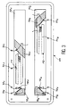
- FIG. 3 shows an embodiment of the surface acoustic wave device.
- This device comprises two similar paths, the elements of which are identified by references bearing the indices 1 and 2 respectively. It suffices to describe one.
- the first path includes a 701 blade serving as a piezoelectric substrate. This blade is preferably made of quartz, with an ST cut.
- the input transducer TR1 is connected to a ground terminal 711 and to an input terminal 721.
- An acoustic absorbent 731 is placed on the left side of the transducer. Only the acoustic wave propagating to the right is therefore used.
- the transducer F1 has one of its electrodes connected to an output terminal 741 and the other to a ground pad 751.
- An acoustic absorbent 761 is disposed at the rear of the output transducer.
- the second channel is similar to the first, except that the second output transducer is offset downstream on its piezoelectric plate, as already explained and that it has been optimized to take into account propagation distortions.
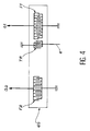
- FIG. 4 another variant of a part of the component of the invention is seen with a single input transducer TR, connected to a single input e. Two surface waves leave this transducer, one on the right towards the output transducer F1, the other on the left towards the output transducer F2, the second being more distant from TR than is the first.
- FIG. 5 represents an embodiment of a component 80 for a transceiver according to the invention.
- the reception channel of this component 80 corresponds to the embodiment of the component for receiver illustrated in FIG. 3.
- FIG. 3 it is understood that it is particularly simple to use the space left free on the piezoelectric plate 70 lame ( top right in Figure 3) to have a third surface acoustic wave filter that can be used for transmission, this filter can be similar to those of the reception channel.
- the emission filter comprises on the piezoelectric plate 701 supporting the first reception channel, an input transducer TR3 connected to a ground terminal 713 and to an input terminal 723, an acoustic absorbent 733 disposed on the right of the transducer, an output transducer F3, one of the electrodes of which is connected to an output terminal 743 and the other to a ground pad 753 and finally, an acoustic absorbent 763 placed at the rear of the transducer exit.
- This acoustic absorbent 763 merges with the acoustic absorbent 761 of the transducer F1 of the first reception channel.
- Component 80 of Figure 5 can be used in a spread spectrum differential transceiver. Because of its perfect symmetry, the component transmits and receives very similar signals so that a certain number of circuits used in the transmission channel can be shared with certain circuits of the reception channel.
- FIG. 6 shows, which shows a differential transceiver according to the invention, at least in its upstream part, up to the component 80, the downstream part being the same as in the figure. 1 (outputs S1, S2, multiplier 38 and baseband stage).
- the differential transceiver of FIG. 6 is characterized by the fact that it comprises the transceiver component 80 which has been described above, this component 80 being used in its transmission path TR3, F3 to produce the signal of intermediate frequency spread spectrum and in its reception channel TR1, F1, TR2, F2 as a device for processing the signal at intermediate frequency capable of correlating with the pseudo-random sequence used on transmission.
- the transceiver of Figure 6 is characterized in that the means 110, 112 of the transmission channel for transposing the intermediate frequency signal into a radio frequency signal are the same as the means of the transmission channel. reception to transpose the radiofrequency signal into an intermediate frequency signal.
- the antenna 100 of the transmission channel it is common with the antenna of the reception channel, this common antenna being connected to the common frequency transposition means 110, 112 by a reception amplifier 1021 and an amplifier 1022 emission in parallel.
- a first switch It is provided for connecting the common antenna 100 either to the reception amplifier 1021, or to the transmission amplifier 1022.
- a second switch I2 is also provided for connecting, in synchronism with the first, either the reception amplifier 1021, or the transmission amplifier 1022 to the common means 110, 112 for signal transposition.
- a bandpass filter 104 can be provided just after the amplifier 1022.
- An automatic gain control circuit 118 is also provided for adjusting the gain of the amplifier 114 from the received signal.
- FIG. 6 clearly shows the use of several subassemblies both on transmission and on reception.
- the transition from transmission mode to reception mode is done using switches I1 to I5. These switches can be diode switches, so that the change from one mode to another takes place quickly. In the diagram in Figure 6, all the switches are in the receive position (R).
- the signal supplied by the antenna is amplified by 1021 and filtered by 106 whose band is equal to or greater than Bes.
- the signal at the output of the mixer 112 is filtered by 106, amplified by 1022 then filtered again by 104 before being emitted by the antenna 100.
- the filter 104 is necessary to avoid any secondary lobe that could be produced by the nonlinearities in the amplifier 1022.
- the mixer 112 operates in downconverter mode in reception mode, that is to say that the signal present at the input is mixed with the signal from the local oscillator and that the frequency of the signal supplied in intermediate frequency is the difference in frequencies between the frequency of the local oscillator and the radio frequency, the intermediate frequency being lower than the frequency of the local oscillator and at the radio frequency, the frequency FI being lower than the frequencies OL and RF.
- the intermediate frequency stages operate as follows in reception mode.
- the signal at intermediate frequency at output 112 is amplified by 114 then filtered by 116, the band of which is greater than Bes, before being injected at the input of component 80, the detailed operation of which has been described above.
- the gain control circuit 118 automatically adjusts the gain 114 so that the power of the intermediate frequency signal at the reception input of the filtered component is constant.
- the signal is applied to the two electrodes of input TR1, TR2 of component 80.
- the two outputs S1 and S2 of the filter are identical except for a delay, the value of this delay is T, duration of the binary symbol transmitted, as already indicated.
- the switches I1 to I5 are in position E.
- the transmission channel of the component 80 is used to produce the transmission signal. This channel is strictly identical to the first reception channel of the same component used in the the only difference is that the impulse response of the transmission channel is the pseudo-random sequence itself and not the pseudo-random sequence reversed in time.
- the surface acoustic wave component F3 therefore makes it possible to directly produce the intermediate frequency signal modulated by the pseudo-random sequence, subject to injecting a very short duration pulse at its input.
- the modulation by the binary data to be transmitted is obtained by reversing the polarity of this pulse.
- the filter F3 therefore has, at its input, positive or negative pulses, depending on the polarity of the data D to be transmitted. These pulses are separated by a time T equal to the duration of the binary symbol. This duration T is obviously also equal to the duration of the impulse response of the filter F3.
- the gain of amplifier 114 is fixed and preset using a potentiometer 120. It is conceivable to use this gain control input of the amplifier 114 to adjust the transmission power either using calibrated voltages or using an automatic gain control loop, the input setpoint would be the signal strength emitted by the antenna.
Landscapes
- Engineering & Computer Science (AREA)
- Computer Networks & Wireless Communication (AREA)
- Signal Processing (AREA)
- Transceivers (AREA)
Applications Claiming Priority (2)
| Application Number | Priority Date | Filing Date | Title |
|---|---|---|---|
| FR9215469 | 1992-12-22 | ||
| FR9215469A FR2696298B1 (fr) | 1992-07-15 | 1992-12-22 | Composant pour récepteur ou pour émetteur-récepteur différentiel de signaux à étalement de spectre par séquence directe et émetteur-récepteur correspondant. |
Publications (2)
| Publication Number | Publication Date |
|---|---|
| EP0604294A1 true EP0604294A1 (de) | 1994-06-29 |
| EP0604294B1 EP0604294B1 (de) | 1999-11-10 |
Family
ID=9436905
Family Applications (1)
| Application Number | Title | Priority Date | Filing Date |
|---|---|---|---|
| EP93403102A Expired - Lifetime EP0604294B1 (de) | 1992-12-22 | 1993-12-20 | Bauelement für differentiellen Sende-Empfänger von Direktsequenz-Spreizspektrumsignalen und entsprechender Sende-Empfänger |
Country Status (4)
| Country | Link |
|---|---|
| US (1) | US5434893A (de) |
| EP (1) | EP0604294B1 (de) |
| JP (1) | JPH077456A (de) |
| DE (1) | DE69326995T2 (de) |
Cited By (1)
| Publication number | Priority date | Publication date | Assignee | Title |
|---|---|---|---|---|
| GB2319936A (en) * | 1996-11-29 | 1998-06-03 | Hitachi Ltd | CDMA communication RF signalling processing apparatus using SAW |
Families Citing this family (10)
| Publication number | Priority date | Publication date | Assignee | Title |
|---|---|---|---|---|
| US5553081A (en) * | 1994-04-08 | 1996-09-03 | Echelon Corporation | Apparatus and method for detecting a signal in a communications system |
| JP3250401B2 (ja) * | 1995-02-07 | 2002-01-28 | 株式会社日立製作所 | 受信機 |
| US5563610A (en) * | 1995-06-08 | 1996-10-08 | Metawave Communications Corporation | Narrow beam antenna systems with angular diversity |
| GB2303265B (en) * | 1995-07-10 | 1998-07-08 | Matsushita Electric Industrial Co Ltd | Spread spectrum communication apparatus,and demodulator,surface acoustic wave element and surface acoustic wave parts for spread spectrum communication |
| CA2186793C (en) * | 1995-11-13 | 2000-12-19 | Vijitha Weerackody | Method and apparatus to implement antenna diversity for direct sequence spread spectrum receivers |
| US6683515B1 (en) * | 1999-09-22 | 2004-01-27 | Matsushita Electric Industrial Co., Ltd. | Surface-acoustic-wave filter providing outputs with different delay times and communications unit |
| US6535545B1 (en) | 1999-10-15 | 2003-03-18 | Rf Waves Ltd. | RF modem utilizing saw resonator and correlator and communications transceiver constructed therefrom |
| JP4371830B2 (ja) * | 2004-01-27 | 2009-11-25 | 富士通株式会社 | 歪補償増幅装置および基地局 |
| US7952482B2 (en) * | 2005-08-25 | 2011-05-31 | University Of Central Florida Research Foundation, Inc. | Surface acoustic wave coding for orthogonal frequency coded devices |
| US7777625B1 (en) * | 2005-08-25 | 2010-08-17 | University Of Central Florida Research Foundation, Inc. | Weighted saw reflector gratings for orthogonal frequency coded SAW ID tags and sensors |
Citations (4)
| Publication number | Priority date | Publication date | Assignee | Title |
|---|---|---|---|---|
| FR2312881A1 (fr) * | 1975-05-29 | 1976-12-24 | Goff Jeannine Le | Demodulateurs differentiels a dispositifs a ondes elastiques de surface |
| US4506239A (en) * | 1982-10-25 | 1985-03-19 | Motorola, Inc. | Compound surface acoustic wave matched filters |
| EP0409538A2 (de) * | 1989-07-20 | 1991-01-23 | AT&T GLOBAL INFORMATION SOLUTIONS INTERNATIONAL INC. | Demodulator für Spreizspektrumsignal |
| EP0474491A2 (de) * | 1990-09-06 | 1992-03-11 | NCR International, Inc. | Verfahren und Einrichtung zur Verarbeitung eines empfangenen Funkdatensignals |
Family Cites Families (5)
| Publication number | Priority date | Publication date | Assignee | Title |
|---|---|---|---|---|
| NO163800C (no) * | 1987-10-19 | 1990-07-18 | Forsvarets Forsknings | Fremgangsmaate for demodulering av data. |
| US5243622A (en) * | 1991-08-02 | 1993-09-07 | General Dynamics Corporation, Electronics Division | Direct-sequence spread-spectrum communication system with asynchronous despreading |
| US5276703A (en) * | 1992-01-13 | 1994-01-04 | Windata, Inc. | Wireless local area network communications system |
| US5289499A (en) * | 1992-12-29 | 1994-02-22 | At&T Bell Laboratories | Diversity for direct-sequence spread spectrum systems |
| US5345472A (en) * | 1993-08-02 | 1994-09-06 | Motorola, Inc. | Method and apparatus for receiving and decoding communication signals in a CDMA receiver |
-
1993
- 1993-12-03 US US08/161,877 patent/US5434893A/en not_active Expired - Lifetime
- 1993-12-20 EP EP93403102A patent/EP0604294B1/de not_active Expired - Lifetime
- 1993-12-20 DE DE69326995T patent/DE69326995T2/de not_active Expired - Lifetime
- 1993-12-22 JP JP5324503A patent/JPH077456A/ja active Pending
Patent Citations (4)
| Publication number | Priority date | Publication date | Assignee | Title |
|---|---|---|---|---|
| FR2312881A1 (fr) * | 1975-05-29 | 1976-12-24 | Goff Jeannine Le | Demodulateurs differentiels a dispositifs a ondes elastiques de surface |
| US4506239A (en) * | 1982-10-25 | 1985-03-19 | Motorola, Inc. | Compound surface acoustic wave matched filters |
| EP0409538A2 (de) * | 1989-07-20 | 1991-01-23 | AT&T GLOBAL INFORMATION SOLUTIONS INTERNATIONAL INC. | Demodulator für Spreizspektrumsignal |
| EP0474491A2 (de) * | 1990-09-06 | 1992-03-11 | NCR International, Inc. | Verfahren und Einrichtung zur Verarbeitung eines empfangenen Funkdatensignals |
Cited By (2)
| Publication number | Priority date | Publication date | Assignee | Title |
|---|---|---|---|---|
| GB2319936A (en) * | 1996-11-29 | 1998-06-03 | Hitachi Ltd | CDMA communication RF signalling processing apparatus using SAW |
| GB2319936B (en) * | 1996-11-29 | 1999-03-24 | Hitachi Ltd | CDMA communication RF signal processing apparatus using SAW |
Also Published As
| Publication number | Publication date |
|---|---|
| DE69326995D1 (de) | 1999-12-16 |
| DE69326995T2 (de) | 2000-06-15 |
| JPH077456A (ja) | 1995-01-10 |
| US5434893A (en) | 1995-07-18 |
| EP0604294B1 (de) | 1999-11-10 |
Similar Documents
| Publication | Publication Date | Title |
|---|---|---|
| EP0803991B1 (de) | Verfahren zur Optimierung von Funkkommunikation zwischen einer Basisstation und einer Mobilstation | |
| EP0314101B1 (de) | Radiofrequenzoptisches Übertragungssystem, besonders für Satellitenfunken | |
| EP0604294B1 (de) | Bauelement für differentiellen Sende-Empfänger von Direktsequenz-Spreizspektrumsignalen und entsprechender Sende-Empfänger | |
| FR2642922A1 (fr) | Dispositif de communication sur spectre disperse | |
| EP3188399B1 (de) | Vollduplex-sender/-empfänger mit einem modul für die nicht reziproke frequenztransposition | |
| EP2074700B1 (de) | Hauptsächlich für die breitband-funkkommunikation bestimmtes radioelektrisches sende- und empfangsmodul | |
| FR2813465A1 (fr) | Methode d'estimation conjointe de canal et de direction d'arrivee | |
| FR2751086A1 (fr) | Procede d'elimination du brouillage mutuel entre au moins deux radars d'un groupement de radars | |
| FR2644953A1 (fr) | Dispositif de communication sur spectre disperse | |
| EP0778678B1 (de) | Differentialempfänger für Direktsequenzspreizspektrumsignale | |
| FR2696298A1 (fr) | Composant pour récepteur ou pour émetteur-récepteur différentiel de signaux à étalement de spectre par séquence directe et émetteur-récepteur correspondant. | |
| EP0138727B1 (de) | Empfangsschaltung für eine mal mit einem Analogsignal frequenzmodulierte und mal mit einem Digitalsignal phasenmodulierte Welle | |
| EP0849889B1 (de) | Verfahren zum Mehrwegesignalempfang | |
| EP1385272B1 (de) | Verfahren zur Übertragung von Information zwischen einem Sender und einem Empfänger mittels Ultra-Breitbandsignalen | |
| EP3471280B1 (de) | Methode zur bestimmung der mehrwegkomponenten eines impulsgesteuerten uwb-kanals | |
| FR2695772A1 (fr) | Composant pour récepteur différentiel de signaux à étalement de spectre par séquence directe. | |
| EP3503413A1 (de) | Multiantennen-impuls-uwb-empfänger | |
| EP0083895B1 (de) | Als Modulator, Mischer und Sende-Empfangsumschalter arbeitende Mikrowellenschaltung und Einrichtungen die eine solche Schaltung benutzen | |
| FR2707441A1 (fr) | Composant pour récepteur ou pour émetteur-récepteur différentiel de signaux à étalement de spectre par séquence directe et émetteur-récepteur correspondant. | |
| FR2659510A1 (fr) | Dispositif de reception d'un spectre disperse. | |
| WO2000028662A1 (fr) | Filtre numerique a architecture parallele et recepteur de signaux a etalement de spectre utilisant un tel filtre | |
| EP1075122A1 (de) | Messung der Stossantwort für einen vom Schlupffaktor abhängigen Pseudo-Zufallscode | |
| EP0859472A1 (de) | Kodemultiplexvielfachzugriffssender | |
| Geller et al. | Comparison between theoretical and actual results for a spread spectrum system in a multipath environment | |
| JP3330510B2 (ja) | 弾性表面波装置及びそれを用いた通信装置 |
Legal Events
| Date | Code | Title | Description |
|---|---|---|---|
| PUAI | Public reference made under article 153(3) epc to a published international application that has entered the european phase |
Free format text: ORIGINAL CODE: 0009012 |
|
| AK | Designated contracting states |
Kind code of ref document: A1 Designated state(s): BE DE ES GB IT NL |
|
| 17P | Request for examination filed |
Effective date: 19941202 |
|
| 17Q | First examination report despatched |
Effective date: 19971217 |
|
| GRAG | Despatch of communication of intention to grant |
Free format text: ORIGINAL CODE: EPIDOS AGRA |
|
| GRAG | Despatch of communication of intention to grant |
Free format text: ORIGINAL CODE: EPIDOS AGRA |
|
| GRAH | Despatch of communication of intention to grant a patent |
Free format text: ORIGINAL CODE: EPIDOS IGRA |
|
| GRAH | Despatch of communication of intention to grant a patent |
Free format text: ORIGINAL CODE: EPIDOS IGRA |
|
| GRAA | (expected) grant |
Free format text: ORIGINAL CODE: 0009210 |
|
| AK | Designated contracting states |
Kind code of ref document: B1 Designated state(s): BE DE ES GB IT NL |
|
| PG25 | Lapsed in a contracting state [announced via postgrant information from national office to epo] |
Ref country code: NL Free format text: LAPSE BECAUSE OF FAILURE TO SUBMIT A TRANSLATION OF THE DESCRIPTION OR TO PAY THE FEE WITHIN THE PRESCRIBED TIME-LIMIT Effective date: 19991110 Ref country code: ES Free format text: THE PATENT HAS BEEN ANNULLED BY A DECISION OF A NATIONAL AUTHORITY Effective date: 19991110 |
|
| REF | Corresponds to: |
Ref document number: 69326995 Country of ref document: DE Date of ref document: 19991216 |
|
| PG25 | Lapsed in a contracting state [announced via postgrant information from national office to epo] |
Ref country code: BE Free format text: LAPSE BECAUSE OF NON-PAYMENT OF DUE FEES Effective date: 19991231 |
|
| ITF | It: translation for a ep patent filed | ||
| GBT | Gb: translation of ep patent filed (gb section 77(6)(a)/1977) |
Effective date: 20000113 |
|
| NLV1 | Nl: lapsed or annulled due to failure to fulfill the requirements of art. 29p and 29m of the patents act | ||
| BERE | Be: lapsed |
Owner name: COMMISSARIAT A L'ENERGIE ATOMIQUE Effective date: 19991231 |
|
| PLBE | No opposition filed within time limit |
Free format text: ORIGINAL CODE: 0009261 |
|
| STAA | Information on the status of an ep patent application or granted ep patent |
Free format text: STATUS: NO OPPOSITION FILED WITHIN TIME LIMIT |
|
| 26N | No opposition filed | ||
| REG | Reference to a national code |
Ref country code: GB Ref legal event code: IF02 |
|
| PGFP | Annual fee paid to national office [announced via postgrant information from national office to epo] |
Ref country code: IT Payment date: 20061231 Year of fee payment: 14 |
|
| PG25 | Lapsed in a contracting state [announced via postgrant information from national office to epo] |
Ref country code: IT Free format text: LAPSE BECAUSE OF NON-PAYMENT OF DUE FEES Effective date: 20071220 |
|
| PGFP | Annual fee paid to national office [announced via postgrant information from national office to epo] |
Ref country code: GB Payment date: 20121128 Year of fee payment: 20 |
|
| PGFP | Annual fee paid to national office [announced via postgrant information from national office to epo] |
Ref country code: DE Payment date: 20121221 Year of fee payment: 20 |
|
| REG | Reference to a national code |
Ref country code: DE Ref legal event code: R071 Ref document number: 69326995 Country of ref document: DE |
|
| REG | Reference to a national code |
Ref country code: GB Ref legal event code: PE20 Expiry date: 20131219 |
|
| PG25 | Lapsed in a contracting state [announced via postgrant information from national office to epo] |
Ref country code: GB Free format text: LAPSE BECAUSE OF EXPIRATION OF PROTECTION Effective date: 20131219 Ref country code: DE Free format text: LAPSE BECAUSE OF EXPIRATION OF PROTECTION Effective date: 20131221 |