EP0604517B1 - Rückgewinnung der tonsignalen von einer optischen aufzeichnung von variabeler breite - Google Patents
Rückgewinnung der tonsignalen von einer optischen aufzeichnung von variabeler breite Download PDFInfo
- Publication number
- EP0604517B1 EP0604517B1 EP92919779A EP92919779A EP0604517B1 EP 0604517 B1 EP0604517 B1 EP 0604517B1 EP 92919779 A EP92919779 A EP 92919779A EP 92919779 A EP92919779 A EP 92919779A EP 0604517 B1 EP0604517 B1 EP 0604517B1
- Authority
- EP
- European Patent Office
- Prior art keywords
- transition
- bias line
- scan
- signal
- opaque
- Prior art date
- Legal status (The legal status is an assumption and is not a legal conclusion. Google has not performed a legal analysis and makes no representation as to the accuracy of the status listed.)
- Expired - Lifetime
Links
- 230000003287 optical effect Effects 0.000 title claims abstract description 54
- 230000005236 sound signal Effects 0.000 title description 31
- 230000002146 bilateral effect Effects 0.000 claims abstract description 61
- 238000011084 recovery Methods 0.000 claims abstract description 26
- 230000007704 transition Effects 0.000 claims description 489
- 230000008859 change Effects 0.000 claims description 40
- 230000009977 dual effect Effects 0.000 claims description 25
- 238000000034 method Methods 0.000 claims description 20
- 230000007547 defect Effects 0.000 claims description 18
- 230000007423 decrease Effects 0.000 claims description 11
- 230000004044 response Effects 0.000 claims description 5
- 230000003252 repetitive effect Effects 0.000 claims 4
- 230000033001 locomotion Effects 0.000 abstract description 15
- 230000000694 effects Effects 0.000 abstract description 8
- 230000009467 reduction Effects 0.000 abstract description 8
- 239000003990 capacitor Substances 0.000 description 14
- 230000009471 action Effects 0.000 description 13
- 230000005855 radiation Effects 0.000 description 12
- 101150117787 outL gene Proteins 0.000 description 11
- 239000000428 dust Substances 0.000 description 10
- 238000012545 processing Methods 0.000 description 9
- 238000010586 diagram Methods 0.000 description 8
- 101100117236 Drosophila melanogaster speck gene Proteins 0.000 description 7
- 238000004458 analytical method Methods 0.000 description 6
- 238000005286 illumination Methods 0.000 description 6
- 238000012937 correction Methods 0.000 description 5
- 102000005962 receptors Human genes 0.000 description 5
- 108020003175 receptors Proteins 0.000 description 5
- XUIMIQQOPSSXEZ-UHFFFAOYSA-N Silicon Chemical compound [Si] XUIMIQQOPSSXEZ-UHFFFAOYSA-N 0.000 description 3
- 230000008901 benefit Effects 0.000 description 3
- 238000011109 contamination Methods 0.000 description 3
- 230000001419 dependent effect Effects 0.000 description 3
- 230000008569 process Effects 0.000 description 3
- 230000002441 reversible effect Effects 0.000 description 3
- 229910052710 silicon Inorganic materials 0.000 description 3
- 239000010703 silicon Substances 0.000 description 3
- 238000006243 chemical reaction Methods 0.000 description 2
- 238000011161 development Methods 0.000 description 2
- 230000004907 flux Effects 0.000 description 2
- 238000009434 installation Methods 0.000 description 2
- 230000004048 modification Effects 0.000 description 2
- 238000012986 modification Methods 0.000 description 2
- 230000001603 reducing effect Effects 0.000 description 2
- 238000005070 sampling Methods 0.000 description 2
- 238000012935 Averaging Methods 0.000 description 1
- 241000590428 Panacea Species 0.000 description 1
- 238000009825 accumulation Methods 0.000 description 1
- 230000006978 adaptation Effects 0.000 description 1
- 238000013459 approach Methods 0.000 description 1
- 238000003491 array Methods 0.000 description 1
- 230000005540 biological transmission Effects 0.000 description 1
- 230000008878 coupling Effects 0.000 description 1
- 238000010168 coupling process Methods 0.000 description 1
- 238000005859 coupling reaction Methods 0.000 description 1
- 230000003247 decreasing effect Effects 0.000 description 1
- 230000002950 deficient Effects 0.000 description 1
- 238000001514 detection method Methods 0.000 description 1
- 238000007599 discharging Methods 0.000 description 1
- 238000001914 filtration Methods 0.000 description 1
- 230000006870 function Effects 0.000 description 1
- 230000006872 improvement Effects 0.000 description 1
- 238000004519 manufacturing process Methods 0.000 description 1
- 238000005259 measurement Methods 0.000 description 1
- 238000001454 recorded image Methods 0.000 description 1
- 230000001360 synchronised effect Effects 0.000 description 1
- 230000009897 systematic effect Effects 0.000 description 1
- 230000001960 triggered effect Effects 0.000 description 1
Images


Classifications
-
- G—PHYSICS
- G11—INFORMATION STORAGE
- G11B—INFORMATION STORAGE BASED ON RELATIVE MOVEMENT BETWEEN RECORD CARRIER AND TRANSDUCER
- G11B20/00—Signal processing not specific to the method of recording or reproducing; Circuits therefor
- G11B20/02—Analogue recording or reproducing
- G11B20/025—Error detection or correction
-
- G—PHYSICS
- G11—INFORMATION STORAGE
- G11B—INFORMATION STORAGE BASED ON RELATIVE MOVEMENT BETWEEN RECORD CARRIER AND TRANSDUCER
- G11B20/00—Signal processing not specific to the method of recording or reproducing; Circuits therefor
- G11B20/00992—Circuits for stereophonic or quadraphonic recording or reproducing
-
- G—PHYSICS
- G11—INFORMATION STORAGE
- G11B—INFORMATION STORAGE BASED ON RELATIVE MOVEMENT BETWEEN RECORD CARRIER AND TRANSDUCER
- G11B20/00—Signal processing not specific to the method of recording or reproducing; Circuits therefor
- G11B20/24—Signal processing not specific to the method of recording or reproducing; Circuits therefor for reducing noise
-
- G—PHYSICS
- G11—INFORMATION STORAGE
- G11B—INFORMATION STORAGE BASED ON RELATIVE MOVEMENT BETWEEN RECORD CARRIER AND TRANSDUCER
- G11B7/00—Recording or reproducing by optical means, e.g. recording using a thermal beam of optical radiation by modifying optical properties or the physical structure, reproducing using an optical beam at lower power by sensing optical properties; Record carriers therefor
- G11B7/002—Recording, reproducing or erasing systems characterised by the shape or form of the carrier
- G11B7/003—Recording, reproducing or erasing systems characterised by the shape or form of the carrier with webs, filaments or wires, e.g. belts, spooled tapes or films of quasi-infinite extent
- G11B7/0032—Recording, reproducing or erasing systems characterised by the shape or form of the carrier with webs, filaments or wires, e.g. belts, spooled tapes or films of quasi-infinite extent for moving-picture soundtracks, i.e. cinema
Definitions
- the invention relates generally to the recovery of an audio information signal from a variable-area optical record and more particularly to the recovery of such a signal from motion picture film variable-area optical soundtracks.
- Variable-area optical soundtracks on motion picture film have been used in substantially their present form since the earliest days of sound-on-film in the cinema. In their earliest form, a single monophonic optical soundtrack was used, the width of the clear area being proportional to the recorded modulation amplitude. Later modifications intended to reduce distortion provided for bilateral and dual bilateral tracks adjacent to each other, carrying the same modulation information and being identical in their pattern. A further modification provides for separately modulating each of the dual bilateral tracks to provide stereophonic reproduction.
- Modern commercial film projectors continue to use essentially the same illumination and light sensing arrangements for reading variable-area optical soundtracks as those that were used in the earliest sound projection equipment: a light source and narrow mechanical slit to provide a line source illumination, with a single photocell for detection or with dual photocells in the case of stereophonic dual bilateral tracks. Silicon solar cells have replaced the vacuum tube photocells originally used.
- a continuing problem in optical soundtrack reproduction is that of achieving a low noise level while providing a wide frequency range.
- the electrical output level of a solar cell or photocell depends not only on the width of the clear area of the soundtrack but also on the transmissivity of the both the clear and the opaque areas of the soundtrack. Variations in the transmissivity of the clear and opaque areas of the soundtrack are reproduced as noise, transmissivity variations in the clear area being the predominant contributor.
- the transmissivity of the clear area of the soundtrack is reduced by dirt and scratches; the transmissivity of the opaque area of the soundtrack is increased by pinholes and scratches.
- the incidence of these transmissivity variations, and hence of print noise is relatively low in a fresh print, but increases with the number of times a print is projected.
- Cooney also suggested that the image of an illuminated slit could be focussed on the soundtrack in the conventional way and that the resulting illuminated area of the soundtrack could be scanned by a television camera-like scanning device.
- U.S. Patent No. 2,485,829 of Holst et al. shows a scanning arrangement using a threshold detector instead of a limiter to reduce noise caused by transmissivity variations.
- the output of the threshold detector was held in one constant voltage state (e.g., at a low voltage), and when the output of the photo cell was above the threshold level, the output of the threshold detector was held in a different constant voltage state (e.g., at a high voltage).
- the threshold detector reduced noise because minor transmissivity changes in either the opaque area or the clear area would not change the photo cell output sufficiently to cross the threshold and cause noise generating transitions in the output of the threshold detector.
- large transmissivity variations such as large specks of dust, scratches, and pinholes, could still contribute noise to the output signal.
- To reduce the possibility of dirt in the clear area from falsely resetting the bistable only a clear-to-opaque transition after which the output of the photo cell remained in its "opaque" state for more than a given amount of time, typically 1% to 5% of the scan period, was allowed to reset the bistable circuit. This arrangement was unable to reduce noise caused by transmissivity variations in the opaque area and by contamination of the opaque to clear and clear to opaque boundary regions.
- the exposure and development parameters which determine the width and shape of the boundary region are chosen so as to minimize distortion when the soundtrack is reproduced by a solar cell.
- the electrical output of the solar cell represents the total light flux reaching the cell as a result of transmission through the opaque area (negligible), the opaque-to-clear boundary region, the clear-to-opaque boundary region, and the clear area.
- the proportional contribution of the two boundary regions to the total light flux is different at each point on the cycle of the waveform. It is also frequency dependent: at short wavelengths, the opaque areas between successive cycles tend to grow together across the narrow clear area between them, thus widening the boundary regions.
- Known scanning systems employing limiters or threshold detectors to reduce noise produce on each scan an output that is proportional to the effective width of the clear area of the soundtrack at the point at which it is scanned. Because the two boundary regions each have finite width, the measured effective width of the clear area (a) depends on the choice of threshold level or limiting level, (b) is different at different points on the cycle of the waveform, and (c) is frequency dependent. Consequently, a fixed threshold level or limiting level can be chosen that gives low distortion at a given frequency and amplitude, but that fixed threshold level will give significant distortion at other frequencies and levels.
- a particularly severe form of distortion afflicts the negative peaks of the recorded waveform.
- the clear area is so narrow that the two boundary regions of the soundtrack overlap and the clear area becomes partially opaque. This effect is exacerbated by the tendency of opaque areas to grow together when the clear area between them is narrow.
- the soundtrack has no area that a scanning system with a fixed threshold or with limiting would interpret as being clear. This results in clipped negative peaks in the audio output of the scanning system. Because the width of the bias line (the bias line is the nominally clear area that always exists between the two halves of a bilateral track) is varied according to the amplitude of the waveform recorded on the soundtrack to minimize the amount of clear area in the soundtrack, negative peak clipping can occur with signals of all levels.
- the invention relates to the recovery of an audio information signal from a variable-area optical record having record indicia disposed substantially symmetrically about a bias line, particularly bilateral optical soundtracks carried on motion picture film.
- the invention in its various aspects, operates in an environment in which a scan signal is obtained by repetitively scanning the optical record, substantially transverse to the bias line.
- Such scanning may be performed in any manner, including, for example, by physical motion or by electrical or optical action, or any combination thereof. Scanning may also be performed, at least in part, by computational operations (such as by digital signal processing techniques).
- Many commonly-used scanning arrangements use a radiation source and one or more radiation receptors or sensors. Such arrangements include those in which the radiation source provides the scanning action, the receptors provide the scanning action, the record carrier provides the scanning action and those in which a combination of radiation source, receptor and/or record carrier activity provides the scanning action. Examples of systems in which the radiation source provides some or all of the scanning action and the receptors provide no scanning action include those having a flying-spot scanner or a deflected beam of light or other radiation for illuminating the record carrier. Further scanning action may be provided by movement of the record carrier.
- An example of a system in which the receptor activity provides some or all of the scanning action and the radiation source provides no scanning action is that in which a source of radiation illuminates the full width of the record carrier, and a scanned sensor, such as an electrically sampled charge-coupled device (CCD) provides the scanning action.
- a source of radiation illuminates the full width of the record carrier
- a scanned sensor such as an electrically sampled charge-coupled device (CCD) provides the scanning action.
- CCD electrically sampled charge-coupled device
- scanning may also be performed at least in part by computational operations (such as by digital signal processing techniques).
- An example is an arrangement in which a digitally encoded image representation of the record carrier is obtained by using one of the aforementioned arrangements to derive an analog video-like image and then converting the analog image to digitally encoded form. The image representation is then scanned in the digital domain using digital signal processing techniques.
- the output of the scanning arrangement is a scan signal from which, after processing according to the invention, at least one analog audio signal is recovered.
- the processing according to the invention may be implemented by the circuitry of the preferred embodiments or by any equivalent thereof, including digital signal processing. Thus, if a digitally encoded image of the record carrier is derived, both the scanning action and the processing action my be done computationally by digital signal processing techniques.
- a threshold is provided that has a minimum level at the bias line of the bilateral soundtrack (or at the bias line of each bilateral soundtrack if there is more than one bilateral soundtrack, as in the case in a dual bilateral soundtrack), and that increases progressively with distance from the bias line.
- the threshold level is high when the scan is at the edge of each soundtrack, falls progressively to a minimum when the scan reaches the bias line, and then increases progressively back to its original high level when the scan is at the other edge of the soundtrack.
- the threshold level falls and rises twice per scan, once on each bilateral soundtrack.
- the threshold may vary linearly with distance from the bias line of each bilateral soundtrack, but a parabolic law is preferred. In both cases, the maximum threshold level can be at between 80% and 110% of the scan signal, 100% being preferred, and the minimum threshold level can be at between 5% and -5% of the scan signal, 0% being preferred, where 0% is the black level of the scan signal and 100% is the peak level of the scan signal.
- the transversely varying threshold level of the invention reduces noise due to transmissivity variations in both the clear and opaque areas of the soundtrack by a greater amount than a fixed threshold level by ensuring that, at each point on the scan of the soundtrack, there is a maximum difference between the threshold level and the normal level of the scan signal at that point on the scan of the soundtrack. This way, the change in the level of the scan signal required to cross the threshold is maximized at all points on the scan of the soundtrack, and the chance that a change in the level of the scan signal caused by a transmissivity variation will be sufficient to cross the threshold is minimized.
- the threshold is high near the edges of the soundtrack, where the film is normally opaque, the level of the scan signal is normally low, and pinholes causing the level of the scan signal to increase are the main form of transmissivity error.
- the high threshold requires that the pinhole be comparatively large for it to be able to transmit enough light to increase the level of the scan signal above the threshold level.
- the threshold is low in the middle of the soundtrack where the film is normally clear, the level of the scan signal is high, and dirt and scratches causing the level of the scan signal to decrease are the main form of transmissivity error.
- the low threshold requires that the piece of dirt or the scratch be comparatively large for it to be able to attenuate the light sufficiently to reduce the level of the scan signal below the threshold level.
- a further benefit of a threshold detector with a transversely varying threshold level according to the invention is that it considerably reduces distortion, especially at high frequencies, and eliminates clipping of the negative peaks of the analog audio signal recovered from the soundtrack.
- a low threshold level near the bias line enables the clear area to be detected, even when the clear area is very narrow and partially opaque.
- the invention also includes circuitry for generating a transversely varying threshold level having minima that accurately track the bias lines of both bilateral soundtracks and is tolerant of film weave and differences in the magnification of the scanner optical system.
- the invention moreover recovers the audio signal from the output of the threshold detector in a way that suppresses noise that would otherwise be generated by transmissivity errors that are sufficiently large to cross the threshold of the threshold detector.
- This aspect of the invention is used in combination with the threshold detector having a transversely varying threshold level as described above.
- the threshold detector having a transversely varying threshold level as described above.
- a two-step process is used to select the one or more transitions representing the true width of the clear area of the soundtrack. First, the following transitions are selected:
- one or more of the four transitions selected in the first step may be selected as the output transition W out having a distance (z) from the bias line according to the following rules: distance (z) is the lesser of ⁇ distance (x) ⁇ and ⁇ distance (y) ⁇ where:
- V out From transition W out there is generated an analog voltage V out that accurately represents the effective width of the clear area of the soundtrack at the point at which it is scanned, despite the presence of large transmissivity variations in either the opaque area, the clear area or the boundary regions between the opaque and clear areas of the soundtrack.
- the second transition selection step is carried out in the voltage domain and the analog output voltage V out is selected directly from voltages representing the distances of the four transitions selected in the first transition selection step from the bias line.
- V a , V b , V c , and V d are generated, each of which is proportional to the distance of one of the four transitions (a) through (d) respectively from the bias line.
- the four voltages are fed into a voltage selector circuit that performs the following logical operation to select directly an analog output voltage V out that is proportional to the effective width of the clear area at the point at which the soundtrack is scanned:
- V out is the lesser of V x and V y where:
- a slightly non-linear relationship between voltage and distance from the bias line may be used to generate the four voltages V a through V d .
- the slope of the voltage-distance curve near the bias line is steeper than at the edges of the soundtrack. This increases the voltages generated from transitions that occur close to the bias line to compensate for the tendency of the opaque areas of the soundtrack to grow together when the clear area is narrow.
- the slope of the voltage-distance curve is about 5% steeper near the bias line than near the edges of the soundtrack.
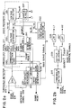
- Figure 1 shows a cross section of the mechanical arrangement of the installation in the optical sound head of a typical projector and a block diagram of the associated electrical circuitry required to generate the scan signal that is decoded by the scan signal decoder circuit of the invention.
- Figure 2a shows a simplified block diagram of a scan signal decoder according to the invention.
- Figure 2b shows a block diagram of a simplified version of the scan signal decoder embodying only the threshold detector with a transversely varying threshold aspect of the invention.
- Figure 2c shows a more detailed block diagram of a scan signal decoder according to the invention.
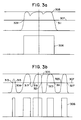
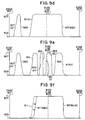
- Figures 3a and 3b show how known scan signal decoders incorporating a threshold detector with a fixed threshold reduces noise compared with a conventional solar cell reproduction system
- Figure 3c shows how a scan signal decoder incorporating a threshold detector with a transversely varying threshold according to the invention reduces noise compared with known scan signal decoders and conventional solar cell reproduction systems.
- Figures 4a through 4c show how a scan signal decoder incorporating a threshold detector with a transversely varying threshold according to the invention reduces clipping distortion on negative peaks compared with known scan signal decoders.
- Figure 5 shows details of the sawtooth ramp generator, timing signal generator and position servos used in connection with generating the transversely varying threshold and the W-wave.
- Figure 6 shows details of the circuits for generating the transversely varying reference level for the threshold detector and the W-wave.
- Figure 7 shows details of the circuits used in the audio recovery aspect of the invention for primary and secondary transition selection.
- Figure 8 is a schematic representation of the voltage selector circuit used in the secondary transition selection stage.
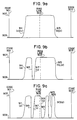
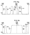
- Figures 9a through 9h show eight examples of how the primary and secondary transition selection stages of the audio recovery circuit according to the invention reduces noise caused by severe transmissivity errors in the soundtrack.
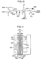
- Figure 10 shows the circuit for generating the left and right bias servo signals used to ensure that the first and second minima of the transversely varying threshold track the bias lines of the left and right bilateral soundtracks, respectively.
- Figure 11 shows a piece of 35 mm motion picture film having a dual bilateral stereo variable-area optical soundtrack.
- Figure 11 shows a piece of 35 mm motion picture film having a dual bilateral variable-area optical soundtrack.
- the dual bilateral soundtrack 001 is located on the film between the sprocket holes, one of which is shown as 003, and picture area 005.
- the dual bilateral soundtrack comprises a first bilateral soundtrack 007 and a second bilateral soundtrack 009 separated by clear septum 011.
- the two bilateral soundtracks are modulated with the same signal and one audio signal is recovered when the film is played.
- the right total audio signal is modulated on first bilateral soundtrack 007
- the left total audio signal is modulated on the second bilateral soundtrack 009
- left total and right total audio signals, R T and L T are recovered when the film is played.
- first bilateral soundtrack 007 will be called the "right track”
- second bilateral soundtrack 009 will be called the "left track”
- right” and “left” refer to the respective audio signals modulated on the tracks rather than the location of the tracks on the film).
- Each bilateral soundtrack comprises a clear area (013 and 015 for the right and left - tracks respectively), bounded by two opaque areas (017 and 019, and 021 and 023 for the right and left tracks respectively)-opaque area 017 of the right track merges with opaque surround 025 of picture area 005.
- a bilateral soundtrack is called bilateral because the width of its clear area (013 and 015 for the right and left tracks respectively) varies symmetrically about the center line of the soundtrack.
- the center line of the soundtrack (shown as broken lines 027 and 029 for the right and left tracks respectively) is called the bias line of the soundtrack. In normal operation, the bias line of the soundtrack never goes completely opaque.
- Figure 1 shows a cross section of the mechanical arrangement of a scanning system in the optical sound head of a typical projector and a block diagram of the associated electrical circuitry required to generate the scan signal that is decoded by the scan signal decoder circuit of the invention.
- the soundtrack is scanned by a linear CCD array 115.
- the standard soundtrack width is 0.076" (1.9 mm), to which must be added about 0.010" (0.25 mm) to allow for track misplacement).
- the illuminated part of the soundtrack must be enlarged before it is focussed on CCD array 115.
- CCD array 115 is placed in the position formerly occupied by the exciter lamp of the conventional optical sound system and magnifying optical system 117 is substituted for the slit and lens assembly of the conventional system.
- CCD array 115 comprises a linear array of 512 pixels, each 14 microns (550 ⁇ ") square.
- a Dalsa IL-C3-0512B CCD array is used.
- a similar device, the Dalsa Inc. model IL-C2-0512 is described in "Ultra High Speed CCD Image Sensors for Scanning Applications" by Brian C. Doody et al, Proceedings of the SPIE - The International Society for Optical Engineering, vol. 1107, pp. 105-116.
- the linear arrangement of the pixels in CCD array 115 serves as the equivalent of the slit of the conventional arrangement.
- Magnifying optical system 117 uses known techniques to focus an image of illuminated soundtrack area 109 approximately two times normal size on CCD array 115.
- the required magnification depends on the length of the CCD array: the magnification and positioning of the magnified soundtrack image on the CCD array should be such that the image of the soundtrack symmetrically covers about 80% of the CCD array's pixels.
- Scanner electronics 119 for the CCD array receives CLOCK and LOAD signals from scan control circuit 127 (to be described in detail below).
- the circuitry of scanning electronics 119 is conventional and will not be described here. Suitable information can be found in the CCD Handbook published by Dalsa, Inc., Waterloo, Canada. It is preferable that, to minimize the emission of radio-frequency interference, scanner electronics 119 be mounted in the sound head in close proximity to CCD array 115.
- elements corresponding to CCD array 115, optical system 117 and associated devices may be configured and dimensioned so that one CCD array is imaged by not only the analog bilateral soundtrack but also digital soundtrack information carried optically between the sprocket holes of the motion picture film.
- a linear CCD array having more than 512 elements would likely be required.
- the linear CCD array is used in combination with motion picture film movement to derive a digitally encoded image of both the analog and digital soundtrack information. Both the underlying analog and digital information may then be recovered computationally from the digitally encoded image.
- the said Seagrave et al applications are incorporated herein in their entirety.
- Clock 125 which, in the preferred embodiment, runs at 27 MHz, provides clock signals for scan control circuit 127.
- Scan control circuit 127 divides down the output of clock 125 to obtain the basic scanning rate for CCD array 115 and provide synchronization signals for the scan decoder circuit that is the subject of the invention and that will be described in detail below.
- Scanning rates in the range of 30-100 kHz can be used for CCD array 115, depending on the bandwidth and freedom from aliasing required. In the preferred embodiment, a scanning rate of about 48 kHz is used.
- the 27 MHz clock rate is divided by 560, giving a scanning rate of 48.214 kHz.
- the division ratio of 560 provides a sequence of 512 clock cycles to clock out the 512 elements of CCD array 115, 32 clock cycles for sampling, during which time the SAMPLE control signal is high, and 16 clock cycles for system reset, during which time the RAMP RESET control signal and its inverse, the IRAMP RESET control signal, are high and low respectively.
- the LOAD control signal goes high for the duration of the 560th clock cycle and resets CCD array 115 for a new scan.
- the preferred scanning rate of about 48 kHz is somewhat higher than the Nyquist rate required for a 20 kHz bandwidth, but the higher scanning frequency is desirable to reduce aliasing caused by components at frequencies higher than 20 kHz present on soundtracks recorded on modern optical recorders.
- Optical soundtracks are not normally recorded with frequencies greater than 20 kHz, but distortion of the recorded image can create harmonics on the film at higher frequencies.
- Mechanical and optical limitations in the recorder, film, and reproducer mean that the amplitude of reproduced supersonic frequencies is relatively low, and falls rapidly with increasing frequency: a scanning rate of about 48 kHz has been found to deal with the aliasing problem adequately.
- the output 129 of CCD array 115 is a video signal comprising a series of pulses at the frequency of the CLOCK signal (27 MHz in the preferred embodiment), each pulse being an analog signal having about 50-60 dB dynamic range and representing the integral of the illumination that fell on the pixel represented by the pulse during the time between scans (i.e., over about 20.7 ⁇ s in the preferred embodiment).
- Using 512 pixels to scan the complete dual bilateral soundtrack does not give sufficient spatial resolution to produce a digital representation of the widths of the clear areas of the soundtrack as accurately as is required for high quality reproduction.
- the desired degree of spatial resolution can be obtained by using the analog content of the output of each pixel. This is done by passing CCD array output 129 through low-pass filter 121 which reconstructs the analog video waveform that would have resulted from a continuous measurement of the transmissivity of the soundtrack across the width of the soundtrack.
- Filter 121 essentially interpolates the transmissivity of the soundtrack at points other than at the center of each of the pixels. Because the soundtrack does not have infinitely sharp boundaries between its opaque areas and its clear areas, the filter can accurately recover all of the information on the soundtrack. The soundtrack boundaries each cover almost three pixels, which results in a spatial oversampling analogous to the frequency oversampling that is required in a time domain sampled system of finite bandwidth to recover all the information in the signal being sampled. Nyquist considerations indicate that fewer pixels could successfully recover all the information in a dual bilateral soundtrack, but the resolution of the next smaller array, which has 256 pixels, is insufficient. Filter 121 is a third-order low-pass filter with a corner frequency of about 24 kHz. Such filters are well known and so will not be discussed further. Filter 121 also removes clock frequency components from the output of CCD array 115.
- the output of filter 121 is connected to the input of AGC and DC restore circuit 123, which applies DC restoration to the video signal at the output of filter 121 so that zero illumination (i.e., the illumination of the CCD array pixels produced by the radiation source 103 (figure 1) illuminating the opaque area of the soundtrack) is represented by signal level of zero volts.
- zero illumination i.e., the illumination of the CCD array pixels produced by the radiation source 103 (figure 1) illuminating the opaque area of the soundtrack
- a different output voltage for zero illumination can be selected if desired.
- AGC and DC restore circuit 123 also normalizes the amplitude of the video signal by the sampling peak amplitude of the video signal, integrating the result over several hundred milliseconds, and adjusting the gain of the video signal to maintain the peak level of the video signal constant.
- the output of AGC and DC restore circuit 123 is scan signal 219.
- AGC and DC restore circuit 123 is desirable because the scan decoder circuit that is the subject of the invention applies parameters that are related to the black level and peak level of the scan signal.
- AGC and DC restore circuit 123 establishes and maintains a constant and known black level and peak level to the scan signal despite changes in the output of radiation source 103, the transmissivity of the clear area of the soundtrack, optical magnification differences, the accumulation of dirt on the optics, and other variables.
- AGC and DC restore circuits are well known in the video art, and so details of the circuit will not be discussed. Other scanning circuits known in the art can be used to produce scan signal 219.
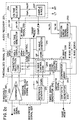
- FIG. 2a A simplified block diagram of the scan decoder that is the subject of the invention is shown in figure 2a.
- Scan signal 219 is connected to the input of threshold detector 215, which, according to the invention, has a transversely varying threshold level.
- the output of threshold detector 215, thresholded signal 217 is ideally a series of pairs of rectangular pulses at the scan rate (48.2 kHz in the preferred embodiment); one pulse of each pair corresponds to the output of the left track, and the other pulse of the pair corresponds to the output of the right track.
- Thresholded signal 217 is fed from threshold detector 215 to audio recovery circuit 221 which recovers from thresholded signal 217 two analog audio signals L T and R T .
- FIG. 3 shows, for simplicity, a single scan of, for instance, the right - track. The rest of the scan, covering the left track, is omitted for clarity.
- scan signal 219, the input of threshold detector 215, is shown as curve 305
- thresholded signal 217 is shown as curve 306.
- Figures 3a and 3b show the input/output relationship of a threshold detector as is already known in the art having a fixed threshold level represented by curve 307.
- Figure 3a depicts a scan of the soundtrack of a new print having neither severe dirt in the clear area nor severe pinholes or scratches in the opaque area.
- Scan signal 219 (curve 305) only crosses fixed threshold level 307 at point 309 corresponding to the boundary between the first opaque area and the clear area, and at point 311 corresponding to the boundary between the clear area and the second opaque area.
- Thresholded signal 217 (curve 306) has only two transitions during the scan, one positive-going (corresponding to an opaque-to-clear boundary in the soundtrack) and one negative-going (corresponding to a clear-to-opaque boundary in the soundtrack).
- Fluctuations in the amplitude of scan signal 219 in the opaque areas and in the clear area are not sufficiently large to cross fixed threshold 307 in either direction, so do not cause additional transitions in thresholded signal 217 (curve 306), and do not contribute noise to the recovered audio signal.
- Figure 3b depicts a scan of the soundtrack of a print that has been projected a number of times, so that dirt and scratches have accumulated on the film.
- scan signal 219 curve 305
- curve 305 further crosses fixed threshold 307 at points 313 and 315 due to a large pinhole in the first opaque area, and at points 317, 319, 321 and 323 due to a smaller and a larger speck of dirt in the clear area, and at points 325 and 327 due to severe scratch in the second opaque area.
- the output of fixed level threshold detector 215 (curve 306) includes several false transitions as well as the two transitions caused by the boundaries of the soundtrack. The additional transitions cause noise in the recovered audio signal.
- Figure 3c depicts a scan of the same piece of worn soundtrack as in figure 3b in which threshold detector 215 has a transversely varying threshold according to the invention.
- Curve 329 shows how the threshold level of threshold detector 215 varies across the width of the soundtrack.
- Scan signal 219 (curve 305) is normally low in the first opaque area, but the large pinhole causes it to increase.
- Transversely varying threshold level 329 is high in the first opaque area, so although the large pinhole causes scan signal 219 to increase, the scan signal does not increase far enough to cross threshold 329. Thus, the pinhole does not cause any transitions in thresholded signal 217 (curve 306) and does not contribute noise to the recovered audio signal.
- Scan signal 219 (curve 305) is normally high in the clear area, but both specks of dust cause it to decrease.
- Transversely varying threshold 329 level is low in the clear area, so although the smaller speck of dust causes scan signal 219 to decrease, the scan signal does not decrease far enough to cross threshold 329. Thus, the smaller speck of dust does not cause any transitions in thresholded signal 217 (curve 306) and does not contribute noise to the recovered audio signal.
- a transversely varying threshold provides a threshold level 329 relative to the normal level of scan signal 219 that, at all points on the scan of the soundtrack, maximizes the change in the normal level of scan signal 219 required to cross the threshold level, and thus minimizes the chance of a transmissivity variation causing a false transition in thresholded signal 217.
- a threshold detector with a transversely varying threshold is not a panacea for noise caused by transmissivity variations: large pieces of dirt and severe scratches can still cause changes in the scan signal sufficiently large to cross the threshold and cause false transitions in the output of the threshold detector.
- the larger speck of dust in the clear area and the severe scratch in the second opaque area cause scan signal 219 to cross threshold 329 at points 321, 323, 325, and 327 respectively, causing corresponding transitions in thresholded signal 217 (curve 306) and contributing noise to the recovered audio signal. Noise caused by such large transmissivity variations is reduced by the audio recovery aspect of the invention described below.
- Figure 4 shows how a threshold detector with a fixed threshold level causes clipping of negative peaks of the waveform recorded on a bilateral optical soundtrack, and how a transversely varying threshold according to the invention substantially reduces the likelihood of such clipping.
- positive-going parts of the waveform are represented by an increase in the clear area
- negative-going parts of the waveform are represented by a decrease in the clear area.
- the width of the clear area is minimal and the clear area is partially opaque because of the gradual boundary between the opaque and clear areas of the soundtrack, and the tendency of opaque areas to grow together across the clear area when the clear area is narrow.
- Figure 4a shows a short piece of, for instance, the right track on which the negative half cycle of a waveform is modulated.
- the figure shows opaque areas 401 and 402, clear area 403, opaque-to-clear boundary 404 and clear-to-opaque boundary 409.
- the track is scanned at points a, b, and c (these are not consecutive scans). Again, the rest of the scan, covering the left track, is omitted for clarity.
- Figure 4b shows scan signal 219 on the three scans of the waveform at points a , b, and c as curves 405a, 405b and 405c.
- the peak level of scan signal 219 on the scan at point c is small compared with that of the scan at point a .
- Figure 4c shows the result of connecting the same three scan signal waveforms 405a, 405b, and 405c to the input of a threshold detector with a transversely varying threshold level according to the invention.
- the level of the transversely varying threshold (curve 429) is low in the region of the bias line, so that even when the level of the scan signal is reduced because of opacity in the bias line region, as in curve 405c, a clear area is nevertheless detected (curve 406c), and the negative peaks of the recovered analog waveform are not clipped.
- transversely varying threshold level that varies linearly across each bilinear soundtrack such that the threshold level is between 5% and -5% at the bias line of each soundtrack, and increases linearly and symmetrically to between 80% and 110% at both edges of the soundtrack (100% is the peak level and 0% is the black level of scan signal 219).
- the transversely varying threshold level has a maximum level of 100% and a minimum level 0%. The minimum of the transversely varying threshold should coincide exactly with the bias line of the bilateral soundtrack.
- the threshold level changes from high to low to high to low to high as the scan proceeds across the full width of the track; and one minimum of the threshold level should coincide exactly with the bias line of the left track, and the other minimum should coincide exactly with the bias line of the right track.
- a further advantage of a threshold detector having a transversely varying threshold level is that it has lower distortion than a threshold detector having a fixed threshold level.
- the transitions detected by a threshold detector having a transversely varying threshold level more accurately represent the instantaneous amplitude of that waveform at the point at which the soundtrack is scanned.
- the audio signal derived from such transitions has considerably lower distortion than if the soundtrack were reproduced by a scanning system using a threshold detector having a fixed threshold level, or by an integrating-type sensor such as a solar cell.
- a further reduction in distortion can be obtained by using a transversely varying threshold level that has an optimized relationship between threshold level and distance from the bias-line. Since the distortion of an optical soundtrack is both amplitude and frequency dependent, an optimized threshold level versus distance from the bias line relationship has to be a compromise.
- the linear relationship described above works well, but lower distortion over a wider range of frequencies can be obtained with a parabolic relationship between threshold level and distance from the bias line, with maximum and minimum levels in the ranges stated above.
- the preferred maximum and minimum levels are about 100% and about 0%, respectively.
- the rate of change of threshold level with distance from the bias line near the bias line is about twice that near the edges of the soundtrack.
- the threshold level changes from high to low to high to low to high as the scan proceeds across the full width of the track; and one minimum of the threshold level should coincide exactly with the bias line of the left track, and the other minimum should coincide exactly with the bias line of the right track.
- Curves 329 and 429 in figures 3 and 4 respectively show a transversely varying threshold level with a parabolic threshold level to distance from the bias line relationship, and a minimum level coinciding with the bias line.
- a threshold detector with a transversely varying threshold level according to a parabolic law also has slightly lower noise than a threshold detector with a transversely varying threshold level according to a linear law because the distance from the edges of the soundtrack at which the threshold level remains high (above 70%, for example) is greater than with the linear law detector. Even some distance from the edges of a soundtrack, the soundtrack is more likely to be opaque than to be clear, so maintaining a high threshold over a greater distance from the edges of the soundtrack provides the most appropriate threshold level to deal with the most common source of transmissivity errors near the edges of the soundtrack, i.e., pinholes and scratches in an opaque area.
- threshold detector 215 comprises video comparator 233 and reference generator 231. Integrated circuits that will serve adequately as video comparator 233 are widely available and this aspect of the circuit will not be described in detail. In the preferred embodiment, an LM 361 video comparator, which has two opposite sense outputs is used.
- Reference signal 229 from reference generator 231 is fed into the reference input of video comparator 233. Twice on each scan of a dual bilateral soundtrack, reference signal 229 changes progressively from its maximum level to its minimum level and back to its maximum level according to a predetermined law, preferably a parabolic law.
- the most important parameter of reference signal 229 is that it should reach its minimum value when the scan passes the bias lines of both of the soundtracks.
- the minima of reference signal 229 must track the two bias lines together as the film weaves, and the distance across the soundtrack between the two minima must be self-adjusting to allow for variations in the magnification of the CCD optical assembly. This saves having to make a precision adjustment of the magnification of the optical assembly on installation. Circuits for generating reference signal 229, and for controlling the generation of reference signal 229 so that it reaches its minimum values when the scan passes the bias lines of both of the soundtracks will be described below.
- Figure 2b shows a simplified version of the scanning system according to the invention, embodying only the threshold detector with the transversely varying threshold aspect of the invention, and using known techniques to recover the analog signals from thresholded signal 217.
- threshold detector 215 produces two pulses on each scan (ignoring the effect of large transmissivity errors), the width of each pulse corresponding to the widths of the clear areas of the right and left tracks respectively.
- the pulse pairs would be fed from threshold detector 215 into output selector gate 223, which, under control of the CENTER and RIGHT (or CENTER and LEFT) control signals generated by W-wave control logic 244 (to be described below in connection with figure 2c), would gate the pulses alternately into left and right outputs, each of which is a pulse-width modulated signal comprising a series of rectangular pulses at the scan rate.
- Left total and right total analog audio signals L T and R T respectively, would be recovered from the two pulse-width modulated signals by integrating them in low-pass filters 225 and 227 respectively.
- a threshold detector with a transversely varying threshold level significantly reduces noise due to transmissivity variations, but is not capable of eliminating such noise altogether.
- the output of the threshold detector, thresholded signal 217 has only two transitions per scan, one corresponding to the opaque-to-clear boundary of the soundtrack, the other to the clear-to-opaque boundary of the soundtrack.
- Transmissivity variations large enough to cause the scan signal to cross the threshold detector threshold cause additional false transitions in the thresholded signal, resulting in noise in the recovered audio signal.
- the audio recovery aspect of the invention recovers the analog audio signal mainly from the transitions that are due to the soundtrack boundaries, and prevents most other, false, transitions in the thresholded signal from contributing noise to the recovered audio signal.
- Audio recovery circuit 221 (figures 2a and 2c) applies the following principles to reject false transitions in thresholded signal 217 caused by large transmissivity errors, to select using a two-stage process at least one transition representing the true width of the clear area of the soundtrack at the point at which it is scanned, and to derive a signal from that at least one transition:
- transition selection logic 249 selects the following four transitions from all of the transitions that occur in the output of threshold detector 219 during the scan:
- a second transition selecting stage selects as the output transition W out having a distance (z) from the bias line, one or more of the four transitions that represent the true width of the clear area of the soundtrack at the point at which it is scanned, and derives an output voltage V out from transition W out .
- the second transition selecting stage selects transition W out according to the following rules: distance (z) is the lesser of ⁇ distance (x) ⁇ and ⁇ distance (y) ⁇ where:
- transitions (a) through (d) are selected with respect to the left track, a first at least one transition W outL , representing the width of the clear area of the left track at the point at which it is scanned is selected from them, and a first voltage V outL is derived from the transition W outL .
- a further four transitions, transitions (e), (f), (g), and (h), corresponding to transitions (a), (b), (c) and (d) respectively, are selected with respect to the right track, a second at least one transition W outR , representing the width of the clear area of the right track at the point at which it is scanned, is derived from them, and a second voltage V outR is derived from the transition W outR .
- audio recovery circuit 221 can be designed to operate in the time domain to implement the above rules and produce a pulse-width modulated signal that, for each soundtrack, produces a single pulse per soundtrack per scan, the width of the pulse being proportional to the width of the clear area of the soundtrack at the point at which it is scanned.
- the following four time differences relating to transitions occurring in thresholded signal 217 would be measured:
- Timing and logic circuits can be devised using principles that are known in the art to perform the operations just described.
- four pulses can be constructed each with a duration equal to one of the four time differences t a through t d , and one of them can be selected according to the above relationship to provide the output pulse.
- the required averaging can be achieved by generating a pulse having a duration equal to the average duration of the pulses to be averaged, and then selecting the generated pulse.
- the circuit produces a series of pulses at the scan frequency, the pulse width being proportional to the width of the clear area of the soundtrack at the point at which the soundtrack is scanned.
- the analog audio signal, L T or R T is recovered from the pulse-width modulated signal by low-pass filtering as discussed above in connection with figure 2b. Transitions from the other bilateral soundtrack can be processed using extra circuitry, or by time multiplexing one set of circuitry between the two tracks.
- Audio recovery circuit 221 shown in figure 2a generates, for each soundtrack, four voltages proportional to the distances of the four transitions from the bias line, and then selects one or more voltages from the set of four voltages to be the output voltage. Generating voltages before the secondary transition selecting stage enables the secondary transition selecting stage to select directly the voltage representative of the width of the clear area of the soundtrack at the point at which it is scanned.
- Audio recovery circuit 221 for a dual bilateral soundtrack comprises transition selection logic 249, voltage generator 255, voltage selector 251, and sample and hold circuit 257, and recovers the two analog audio signals, L T and R T .
- Transition selection logic circuit 249 performs the primary transition selection and receives thresholded signal 217, EDGE control signals, and SCAN POINT control signals from timing signal generator 242. Transition selection logic circuit 249 generates two groups of four hold signals, hold signals 245a through 245d for the left track and hold signals 245e through 245h for the right track. Hold signals 245a through 245h are all in one state at the beginning of each scan, and change state progressively as the scan proceeds and transitions (a) through (h) respectively occur.
- the control signals from timing signal generator 242 inform transition selection logic circuit 249 of the position of the scan across the width of the dual bilateral soundtrack so that, for instance, hold signals 245a and 245c, corresponding to transitions (a) and (c) respectively, can only change state when the scan is between the edge and the bias line of the left track.
- Voltage generator 255 receives the two groups of four hold signals 245a through 245h and W-wave signal 239 and generates two groups of four analog voltages, voltages V a through V d for the left track and voltages V e through V h for the right track. Each of the eight outputs of voltage generator 255 follows W-wave signal 239 until the respective hold signal 245a through 245h changes state, after which it remains constant at the level of the W-wave signal at the instant that the hold signal changed state.
- Hold signals 245b, 245d, 245f, and 245h which correspond to last transitions, may later in the scan, after they have changed state once, change back to their original state (indicating that the transition previously detected was not the last transition), causing the corresponding output of voltage generator 255 to resume following W-wave signal 239 until the hold signal once more changes state.
- all eight outputs of voltage generator 255 should be constant.
- V a through V d are proportional to the distances of the transitions (a) through (d) from the bias line of the left track and voltages V e through V h are proportional to the distances of transitions (e) through (h) from the bias line of the right track.
- Voltage generator 255 is described in detail below.
- the two groups of four analog voltages generated by voltage generator 255 are fed into voltage selector circuit 251 which performs the secondary transition selection in the voltage domain by selecting one of the four voltages V a through V d to be the analog output voltage V outL for the left track and selecting one of the four voltages V e through V h to be the analog output voltage V outR for the right track according to the following relationships:
- V outL is the lesser of V x and V y where:
- voltages V e through V h are substituted for voltages V a through V d
- voltage V outR is substituted for V outL .
- the analog output voltage is a direct measure of the width of the clear area of the respective bilateral soundtrack at the point at which the dual bilateral soundtrack is scanned.
- Voltage selector circuit 251 is described in detail below.
- analog output voltages V outL and V outR are fed into sample and hold circuit 257, which generates left and right total analog output signals L T and R T respectively.
- sample and hold circuit 257 updates left and right total analog output signals L T and R T with the new values of analog output voltages V outL and V outR respectively at the end of every scan.
- the left total and right total analog output signals should be subject to a first sin x/x correction to correct for the scan rate of the scanning system, and a second sin x/x correction to correct for the non-zero height of the pixels of CCD array 115 (figure 1).
- a first sin x/x correction to correct for the scan rate of the scanning system
- a second sin x/x correction to correct for the non-zero height of the pixels of CCD array 115 (figure 1).
- the second correction is considerably greater than the first, a single pixel height slit loss correction (analogous to slit-loss correction in conventional systems) will suffice in all but the most critical applications.
- voltage generator 255 instead of generating eight voltages V a through V h in parallel, generates four voltages V a through V d during the first half of the scan, and then uses the same circuitry to generate the other four voltages V e through V h during the second half of the scan.
- This enables the analog circuitry of voltage generator 255 to be simplified, although the complexity of transition selection logic 249 must be increased to multiplex eight parallel hold signals into two sequences of four parallel hold signals.
- This approach also allows the complexity of voltage selector circuit 251 to be halved; voltage selector 251 selects analog output voltage V outL during the first half of the scan and selects analog output voltage V outR during the second half of the scan.
- the part of sample and hold 257 generating the left total analog output voltage L T is clocked at the mid-point of the scan and the part of sample and hold 257 for the right total analog output voltage R T is clocked at the end of the scan.
- the output of CCD array 115 can be fed into a video digital to analog convertor, the digital output of which is stored in random-access memory.
- the digital representation of the output of CCD array 115 stored in memory is then processed using a digital signal processing circuit programmed to perform the functions of the analog circuitry described above to recover, after digital to analog conversion, one or more analog output signals.
- the digital representation of the output of CCD array 115 stored in memory can be examined by means of a computer for transitions according to a transversely varying threshold, and the resulting transitions selected according to a 2-step process as described above to generate representations of the distance of the soundtrack boundaries from the respective bias lines, from which representations one or more analog signals can be computed.
- One or more analog output signals can then be produced by digital to analog conversion.
- CCD array 115 purely for practical considerations relating the printed circuit layout, scans the right track before the left track.
- Timing signal generator 242 comprises sawtooth generator 235, comparator array 243 and W-wave control logic circuit 244 and generates the SCAN POINT control signals and the EDGE control signals used by transition selection logic circuit 249, and the UP and DOWN control signals used by reference signal generator 231 and W-wave generator 241.
- Sawtooth generator 235 generates a sawtooth signal, the level of which falls linearly from about 6V to zero during the scan and is rapidly returned to its starting voltage at the end of the scan by the RAMP RESET pulse from scan controller 127 (figure 1).
- the output of sawtooth generator 235 is fed into comparator array 243 which generates the five SCAN POINT control signals RIGHT, RBIAS, CENTER, LBIAS, and LEFT, which change state when the scan passes the edge of the right track, the bias line of the right track, the septum between the tracks, the bias line of the left track, and the edge of the left track respectively.
- the SCAN POINT control signals and the EDGE control signals derived from the SCAN POINT control signal by W-wave control logic circuit 244, control transition selection logic circuit 249.
- W-wave control logic circuit 244 also generates from the EDGE control signals the UP and DOWN control signals that control reference generator 231 and W-wave generator 241.
- Comparator array 243 comprises four CMOS invertors operating as comparators 501 through 507.
- the four invertors are part of a hex package; they are on the same chip and thus have well-matched threshold voltages.
- the inputs of comparators 501 through 507 are connected to a chain of five resistors 509 through 517 connected between positive DC supply 519 and negative DC supply 521. This arrangement causes the input voltages of comparators 501 through 507 to be offset from one another; the values of resistors 509 through 517 are chosen so that the voltage differences between successive pairs of comparator inputs are all equal.
- the output of sawtooth generator 235 is connected to nodes 523 and 525.
- Exact synchronization between the time that the RBIAS control signal goes high and the time the scan passes the bias line of the right track and between the time that the LBIAS control signal goes high and the time the scan passes the bias line of the left track is achieved by the LEFT BIAS SERVO signal and the RIGHT BIAS SERVO signal, generated by position error signal generator 253 which will be described below.
- the LEFT BIAS SERVO signal is a measure the asymmetry of the transitions caused by the opaque-to-clear boundary and the clear-to-opaque boundary farthest from the bias line of the left track
- the RIGHT BIAS SERVO signals is a measure the asymmetry of the transitions caused by the opaque-to-clear boundary and the clear-to-opaque boundary farthest from the bias line of the right track.
- the sense of the SERVO signals is such that if the transitions are asymmetrical (indicating that the LBIAS and RBIAS control signals are not going high synchronously with the scan passing the respective bias lines), they introduce appropriate offsets into the inputs of comparators 501 through 507 that change the timing of the LBIAS, CENTER, RBIAS, and RIGHT control signals and correct the asymmetry.
- Capacitor 527 allows the offset to the inputs of comparator array 243 to change rapidly if both LEFT and RIGHT BIAS SERVO signals are similar, as they are when the asymmetry errors are due to film weave. Capacitor 527 allows the inputs of comparator array 243 to change slowly with respect to one another if the LEFT and RIGHT BIAS SERVO signals are different from one another, as they are when there is an error in the magnification of the CCD optical assembly, or a systematic positioning error in the film soundtrack. The LEFT and RIGHT BIAS SERVO signals do not change the equality of the voltage differences between the inputs of successive pairs of comparators, however.
- Control signals EDGE1 through EDGE4 are normally high except as follows: Signal Signal is Low when the Scan is Between EDGE1 right track edge and right track bias line EDGE2 right track bias line and septum EDGE3 septum and left track bias line EDGE4 left track bias line and left track edge Thus, on each of the four linear parts of the W-wave 239, one of the EDGE signals is in its low condition.
- NAND gate 547 which operates as an inverse logic NOR gate.
- the output of gate 547 provides the DOWN control signal which is low except when either EDGE1 or EDGE3 is low.
- Signals EDGE2 and EDGE4 are fed into NAND gate 549 which operates as an inverse logic NOR gate.
- the output of gate 549 provides the UP control signal which is low except when either EDGE2 or EDGE4 is low.
- the UP and DOWN control signals control the operation of reference generator 231 and W-wave generator 241.
- Reference generator 231 comprises two equal and opposite current generators 602 and 604 feeding integrator 606 through analog switches 608 and 610. Analog switches 608 and 610 are controlled by the UP and DOWN control signals respectively.
- first current generator 602 is taken from the collector of transistor 601
- second current generator 604 is taken from the collector of transistor 603.
- a current mirror arrangement comprising transistors 605, 607, and 609 and their associated passive components, ensures that the currents produced by current generators 602 and 604 are equal and opposite.
- Integrator 606 is formed around amplifier 611. Because W-wave generator 241 must be capable of rapidly charging and discharging several capacitors, the current drive capability of amplifier 611a is enhanced by an output stage comprising transistors 637 and 639 and their associated components. For the purposes of analyzing W-wave generator 241, node 617 can be regarded as the output of amplifier 611a. Capacitor 619 between the output and the inverting input of amplifier 611 gives amplifier 611 an integrating characteristic.
- the outputs of current generators 602 and 604 are a.c. coupled into integrator 606 by coupling capacitor 623 and the DC conditions of integrator 606 are defined by feedback resistor 621, which gives integrator 606 a leaky characteristic.
- the output waveform distortion resulting from integrator 606 having a leaky characteristic is acceptable in reference generator 231 but cannot be tolerated in W-wave generator 241.
- W-wave generator 241 the outputs of current generators 602a and 604a are DC coupled into integrator 606a, and DC conditions are set by a feedback loop from the output of W-wave generator 241 to comparator array 243.
- the output of W-wave generator 241 is connected to one input of CMOS NAND gate 533.
- the LBIAS control signal which is connected to the other input of gate 533, holds the output of gate 533 high until the LBIAS control signal goes high, i.e., after the scan passes the bias line of the left track. After the LBIAS control signal goes high, the output of gate 533 can go low when the level of W-wave signal 239, divided by resistors 551 and 539 exceeds the threshold of gate 533.
- the level of W-wave signal 239 increases from its minimum value until it, divided by resistors 551 and 539, exceeds the threshold of gate 533, which causes the gate to change state and, via gates 535 and 549, switch analog switch 610a OFF. This causes the level of W-wave signal 239 to remain constant, because analog switch 608a is already OFF, until the start of the next scan.
- Gate 535 and resistor 539 provide positive feedback so that gate 533 rapidly latches into its changed state once it starts to change.
- Gate 533 also produces an inverted LEFT control signal; CMOS X-NOR gate 537 inverts the output of gate 533 so that the LEFT control signal has the same sense as the RIGHT control signal.
- the output of current generator 602 which causes the output voltage of integrator 606 to decrease (integrator 606 is inverting), is connected to the input of integrator 606 via analog switch 608 controlled by the DOWN control signal.
- the output of the current generator 604 which causes the output voltage of integrator 606 to increase, is connected to the input of integrator 606 via analog switch 610 controlled by the UP control signal.
- the UP control signal is high, the output voltage of integrator 606 increases.
- neither the UP nor the DOWN control signal is high, the output voltage of integrator 606 remains constant.
- analog switch 608 When analog switch 608 is open, the output of current generator 602 goes to ground through diode 613 and resistor 641, and when analog switch 610 is open, the output of the current generator 604 comes from ground via diode 615 and resistor 641.
- Analog switch 625 is switched OFF at the end of each scan by the IRAMP RESET control signal going low. This ensures that no current is fed into integrator 606 as a result of any spurious changes of the UP and DOWN control signals during the reset period.
- Current generator 604 causes the output voltage of integrator 606 to increase, at the same rate at which it decreased in the previous part of the cycle.
- the output voltage of integrator 606 reaches a minimum at the point at which the RBIAS control signal changes state, i.e., at the point at which the scan passes the bias line of the right track.
- the output of integrator 606 increases until the output of sawtooth generator 235 falls to the level at which it causes the CENTER control signal to change state. This causes both the UP and the DOWN control signals once more to change state, switching analog switch 608 ON and analog switch 610 OFF.
- Current generator 602 once more causes the output voltage of integrator 606 to decrease until the output of sawtooth generator 235 reaches the level at which it causes the LBIAS control signal to change state. This causes both the UP and the DOWN control signals to change state for a third time, switching analog switch 608 OFF and analog switch 610 ON.
- Current generator 604 causes the output voltage of integrator 606 to increase once more. The output voltage of integrator 606 once more reaches a minimum, this time when the LBIAS control signal changes state, i.e., at the point at which the scan passes the bias line of the left track.
- the output voltage of integrator 606 increases until it, divided by resistors 539 and 551 (figure 5), reaches the threshold of the comparator formed by gates 533 and 535 (figure 5) changes state (at the point at which the scan passes the edge of the left track), which holds the output voltage of integrator 606 constant for the rest of the cycle of sawtooth generator 235, as described above.
- the current output of current generators 602 and 604 is determined by the voltage on the base of transistor 601 (and, via the current mirror comprising transistors 607 and 609, the voltage of the base of transistor 603) which is determined by the positive supply voltage divided by resistors 627 and 629, and by the output of integrator 606, coupled by capacitor 631 and divided by resistor 633 and the parallel combination of resistors 627 and 629.
- the effect of feeding back the output of integrator 606 via resistor 633 is to increase the output of current generators 602 and 604, and hence the rate of change of the output of integrator 606, as the output of integrator 606 goes more negative. Because the feedback is a.c. coupled, only the instantaneous slope of the output of integrator 606 is changed; its average slope, and hence its symmetry, are unchanged. This gives the output of reference voltage generator 231 its desired parabolic characteristic.
- W-wave generator 241 were required to produce an output waveform that had a pure linear relationship between voltage and distance from the bias lines, it would not include feedback capacitor 631a and resistor 633a.
- increasing the slope of the waveform in the region of the bias line by including feedback resistor 633a, and thereby introducing a deliberate but slight non-linearity into voltage generator 255 (figure 2c) reduces distortion caused by the tendency of the opaque areas to grow together in the vicinity of the bias line.
- the tendency of the opaque areas to grow together moves the opaque-to-clear and clear-to-opaque transitions closer to the bias line than they should be, which results in an insufficient voltage being generated, and causes distortion on negative peaks of the waveform.
- resistor 633a was chosen to increase the slope of W-wave signal 239 near the bias line by about 5% relative to the slope near the edges of the track.
- audio recovery circuit 221 for recovering the left total audio signal L T from the left track. All references to track, bias line, edge, etc. refer to the left track, the bias line of the left track, and the edge of the left track remote from the septum, etc.
- the audio recovery circuit for the recovering the right total audio signal R T from the right track is identical, except for some differences in transition selection logic circuit 249, which will be described below.
- transition selection logic circuit 249 which will be described below.
- an opaque-to-clear transition produces a positive-going transition in thresholded signal 217 and a clear-to-opaque transition produces a negative-going transition.
- Interchanging thresholded signal 217 and inverse thresholded signal 217a (figure 2c) will make the circuit work if threshold detector 215 generates opposite-sense transitions.
- Audio recovery circuit 221 comprises a primary transition selecting circuit (transition selection logic circuit 249) and a secondary transition selecting circuit (voltage generator 255 and voltage selector 251).
- Transition selection logic circuit 249 will now be described with reference to figure 7. On each scan, transition selection logic circuit 249 receives thresholded signal 217, inverse thresholded signal 217a, the four EDGE control signals, the five SCAN POINT control signals, and the IRAMP RESET signal to generate four hold signals 245a through 245d.
- Each hold signal has two states, TRACK and HOLD. When a hold signal is in its TRACK state, the respective output of voltage generator 255 (which will be described in detail below) follows W-wave signal 239; when a hold signal is in its HOLD state, the respective output of voltage generator 255 remains constant at the level of W-wave signal 239 at the instant that the hold signal changed state.
- the hold signals change state synchronously with the following transitions in thresholded signal 217:
- Hold signal 245a is taken from the Q ⁇ output of D-type bistable circuit 709. At the beginning of the scan, hold signal 245a is in its TRACK (high) state as a result of the IRAMP RESET control signal connected to the RESET input of bistable 709 going low at the end of the previous scan. During the scan, the D input of bistable 709 is held low by the CENTER control signal while the right track is being scanned. Any positive-going transitions in thresholded signal 217, which is connected to the CLOCK input of bistable 709, keep hold signal 245a in its TRACK state. After the scan passes the septum and starts scanning the left track, the CENTER control signal, and hence the D input of bistable 709, go high. Then, the first positive-going transition in the output of threshold detector 215 clocks the Q ⁇ output of bistable 709 low state, and hence hold signal 245a into its HOLD state.
- the EDGE4 control signal is connected to the SET input of bistable 709.
- the EDGE4 control signal goes low, maintaining hold signal 245a in its HOLD state for the rest of the scan. If, due to overmodulation (clipping) of the soundtrack, or for some other reason, the scan reaches the bias line without there being a positive-going transition in thresholded signal 217, and hold signal 245a is still in its TRACK state, the EDGE4 control signal changing state when the scan passes the bias line drives hold signal 245a into its HOLD state.
- Hold signal 245b is taken from the Q ⁇ output of bistable 713.
- Bistable 713 operates in a similar manner to bistable 709, with the following three exceptions: (a) inverse thresholded signal 217a is connected to the CLOCK input of bistable 713, so that a clear-to-opaque boundary produces the positive-going clock edge required by bistable 713; (b) the LBIAS control signal, which is high only after the scan passes the bias line, is connected to the D input; and (c) the LEFT control signal, which goes high when scan reaches the edge of the track, is connected through gate 715 acting as an invertor to the SET input of bistable 713.
- the LEFT control signal changing state when the scan reaches the edge of the track drives hold signal 245b into its HOLD state.
- Hold signal 245c is taken from the output of 2-input NOR gate 711.
- the EDGE3 control signal connected to one of the inputs of gate 711 keeps hold signal 247c in its HOLD state except when the scan is between the septum and the bias line.
- hold signal 247c is the inverse of thresholded signal 217.
- a positive-going transition in thresholded signal 217 drives hold signal 245c into its HOLD state. If, subsequently, before the scan reaches the bias line, thresholded signal 217 goes low once more, this switches hold signal 245c back into its TRACK state. Another positive-going transition in thresholded signal 217 returns hold signal 245c to its HOLD state. If the scan reaches the bias line without there being another positive-going transition in thresholded signal 217, hold signal 245c is switched into its HOLD state by the EDGE3 control signal going high when the scan passes the bias line.
- Hold signal 245d is taken from the output of 2-input NOR gate 719.
- the EDGE4 control signal is connected to one of the inputs of gate 717, thresholded signal 217 is connected to the other.
- the output of gate 717 is connected to one of the inputs of 2-input NOR gate 719, and the LEFT control signal, which remains low until the scan passes the edge of the track, is connected to the other.
- the EDGE4 control signal keeps hold signal 245d in TRACK, until the scan reaches the bias line. Then, the EDGE4 control signal goes low, and the output of gate 717 becomes the inverse of thresholded signal 217.
- Hold signal 245d the output of gate 719, is the inverse of the output of gate 717, i.e., is the same as thresholded signal 217.
- a negative-going transition in thresholded signal 217 drives the output of gate 717 high, the output of gate 717 low, and hold signal 245 into its HOLD state.
- thresholded signal 217 goes high once more, corresponding to an opaque-to-clear boundary, hold signal 245d reverts to its TRACK state. Another negative-going transition in thresholded signal 217 returns hold signal 245d to its HOLD state. If the scan reaches the bias line without there being another negative transition in thresholded signal 217, and hold signal is still in its TRACK state, hold signal 245d is switched into its HOLD state by the LEFT control signal going high when the scan passes the edge of the track.
- Hold signals 245e through 245h for the right track are generated by circuits that are almost identical to the ones just described. The differences are as follows:
- Voltage generator 255 receives W-wave signal 239 from W-wave generator 241 and hold signals 245a through 245d.
- Voltage generator circuit 255 comprises four individual track-and-hold circuits 247a through 247d that generate, on each scan, four analog voltages V a through V d respectively by tracking W-wave signal 239 from the beginning of each scan until the respective hold signals 245a through 245d change state. Details of track-and-hold circuits 247a through 247d are shown in figure 7. Since all four track-and-hold circuits are identical, only track-and-hold circuit 247a, which generates voltage V a , will be described. In figure 7, corresponding components for track-and-hold circuits 247b through 247d are indicated by the letters b through d respectively on their designations.
- analog switch 703a selectively connects W-wave signal 239 (figure 2) to capacitor 705a.
- the combined impedance of analog switch 703a, buffer resistor 635 (figure 6) and the output impedance of integrator 606a are sufficiently low that, when analog switch 703a switched ON, the voltage on capacitor 705a accurately follows W-wave signal 239.
- the output of track-and-hold circuit 247a is derived from capacitor 705a via buffer amplifier 707a, which preferably has unity gain and has a sufficiently high input impedance that the output voltage of track-and-hold circuit 247a remains constant at least over the 21 ⁇ s duration of a scan, when analog switch 703a is switched OFF.
- analog switch 703a When hold signal 245a is its TRACK state, analog switch 703a is switched ON, track-and-hold 247a is in TRACK mode, and its output voltage accurately follows W-wave signal 239; when hold signal 245a is in its HOLD state, analog switch 703a is switched OFF, track-and-hold 247a is in HOLD mode, and its output voltage remains constant at the level of W-wave signal 239 at the instant that hold signal 245a switched into its HOLD state.
- hold signal 245a switches track-and-hold 247a into TRACK at the beginning of the scan, and switches it to HOLD mode at the point on the scan at which the first (i.e., farthest from the bias line) positive-going transition occurs in thresholded signal 217. If, due to overmodulation (clipping) of the soundtrack, or for some other reason, the scan reaches the bias line without there being a positive-going transition in the output of threshold detector 215, and track-and-hold 247a is still in TRACK, voltage V a is set to the minimum value of W-wave signal 239 by hold signal 245a changing to its HOLD state when the scan passes the bias line.
- Track-and-hold 247b which generates voltage V b , operates similarly to track-and-hold 245a, except it switches into HOLD mode at the point on the scan after the scan has passed the bias line at which the first (i.e., closest to the bias line) positive-going transition occurs in inverse thresholded signal 217a. If the scan reaches the edge of the track without there being a positive-going transition in the inverse thresholded signal 217a, and track-and-hold 247b is still in its TRACK mode, V b is set to the level of W-wave signal 239 corresponding to the edge of the track (i.e., a high level) by hold signal 245b changing into its HOLD state when the scan passes the edge of the track.
- Hold signal 245c switches track-and-hold 247c, which generates voltage V c , into its TRACK mode when the scan reaches the septum.
- hold signal 247c is the inverse of thresholded signal 217.
- a positive-going transition in thresholded signal 217 drives hold signal 245c into its HOLD state, and switches track-and-hold 247c into its HOLD mode. If, subsequently, before the scan reaches the bias line, thresholded signal 217 goes high once more, switching hold signal 245c into its TRACK state and track-and-hold 247c into its TRACK mode, the output of track-and-hold 247c changes very rapidly to catch up with the current level of W-wave signal 239.
- Another negative-going transition in thresholded signal 217 returns track-and-hold 247c to its HOLD mode. If the scan reaches the bias line without there being another negative-going transition in thresholded signal 217, V c is set to the minimum value of the W-wave by hold signal 245c changing into its HOLD state when the scan passes the bias line.
- Hold signal 245d switches track-and-hold 247d, which generates voltage V d , into its TRACK mode at the beginning of the scan, where it remains until the scan passes the bias line. Then, hold signal 245d becomes the same as thresholded signal 217. Thus, a negative-going transition in thresholded signal 217 (corresponding to a clear-to-opaque boundary) drives hold signal 245 into its HOLD state, switching track-and-hold 247d to HOLD.
- thresholded signal 217 If, subsequently, before the scan reaches the edge of the track, thresholded signal 217 goes high once more, corresponding to an opaque-to-clear boundary, track-and-hold 247d reverts to its TRACK mode, and the output voltage of track-and-hold 247d changes very rapidly to catch up with the current level of W-wave signal 239. Another negative-going transition in thresholded signal 217 returns track-and-hold 247d to its HOLD mode.
- V d is set to the level of W-wave signal 239 at the edge of the track (i.e., a high value) by hold signal 245d changing into its HOLD state when the scan passes the edge of the track.
- FIG. 8 is a schematic representation of the part of voltage selector circuit 251 for selecting the analog output voltage V out from the four voltages V a through V d according to the relationships stated above.
- the other part of voltage selector circuit 251 for selecting analog output voltage V outR from the four voltages V e through V h is identical and will not be described.
- Voltage V a is connected to diode means 801 and voltage V b is connected to diode means 803.
- Voltage V c is connected to diode means 805 and voltage V d is connected to diode means 807.
- Small-signal silicon diodes are preferably used for diode means 801, 803, 805, and 807. To simplify the following analysis, the forward voltage drop of such diodes will be ignored.
- the cathode of diode means 801 is connected to the cathode of diode means 803 at node 809; also connected to node 809 is resistor 813, the other end of which is connected to the negative supply voltage, and the input of buffer amplifier 817.
- the current through resistor 813 forward biases at least one of diode means 801 and 803.
- Diode means 801 and 803 and resistor 813 form a diode gate in which, if voltage V a is greater than voltage V b , diode means 801 is conducting, diode means 803 is reverse biassed, and the voltage at node 809 is the same as voltage V a ; if voltage V b is greater than voltage V a , the voltage at node 809 is the same as voltage V b ; and, if voltages V a and V b are substantially equal to one another, both diode means 801 and 803 conduct, and the voltage at node 809 is the "average" of voltages V a and V b .
- Buffer amplifier preferably has unity gain, in which case the voltage V x at its output, node 821, is the same as at node 809.
- Diode means 805 and 807, resistor 815 and buffer amplifier 819 are interconnected similarly to diode means 801 and 803, resistor 813 and buffer amplifier 817.
- Diode means 805 and 807 and resistor 815 form a diode gate in which, if voltage V c is greater than voltage V d , the voltage V y at node 823, the output of buffer amplifier 819, is the same as voltage V c ; if voltage V d is greater than voltage V c , the voltage at node 823 is the same as voltage V d ; and if voltages V c and V d are substantially equal, the voltage at node 623 is the "average" of voltages V c and V d .
- Nodes 821 and 823 are connected to node 829 via diode means 825 and 827 respectively.
- Diode means 825 and 827 are the same as diode means 801 through 807, but are connected in the opposite sense, i.e., their anodes are interconnected.
- resistor 831 Also connected to node 829 is resistor 831, the other end of which is connected to the positive voltage supply, and the input of buffer amplifier 833. Current flowing through resistor 831 forward biases at least one of diode means 825 and 827.
- Diode means 825 and 827 and resistor 831 form a diode gate in which, if voltage V x is less than voltage V y , diode means 825 is conducting, diode means 827 is reverse biassed, and the voltage at node 829 is the same as voltage V x ; if voltage V y is less than voltage V x , the voltage at node 829 is the same as voltage V y ; and if voltages V x and V y are substantially equal, the voltage at node 629 is the "average" of voltages V x and V y .
- Buffer amplifier 833 preferably has unity gain, in which case the voltage V out at the output 835 of buffer amplifier 833 is the same as the voltage at node 829.
- the greater than/less than characteristic of voltage selector circuit 251 is modified when respective voltage pairs are substantially equal to enable the circuit to comply with rule 5 above.
- Substantially equal voltages appear at the inputs of the diode gates of voltage selector 251 (such as the diode gate formed by diodes 801 and 803, and resistor 813) when two transitions, one in each direction, occur symmetrically about the bias line.
- the output voltage be derived from the average of voltages proportional to the distances of both boundaries of the bilateral soundtrack from the bias line, since this reduces boundary-generated noise by up to 3 dB.
- each example shows thresholded signal 217, the output of threshold detector 215, on one scan of one bilateral soundtrack.
- positions 901 and 903 of both edges of the track are shown in each of the drawings.
- the calculated position of the bias line (broken line 905) and the two voltage states of the threshold detector output, high voltage state 907 corresponding to the clear area of the soundtrack, and low voltage state 909 corresponding to the opaque area of the soundtrack.
- Opaque-to-clear transition 911 and clear-to-opaque transition 913 are caused by the boundaries of the soundtrack; all other transitions are caused by defects as described.
- the transitions are designated (a), (b), (c), and (d) according to the naming convention adopted above. "Before” and "after” the bias line refers to the progress of the scan.
- Figure 9a shows a scan of a soundtrack having neither severe dirt in the clear area nor severe pinholes or scratches in the opaque area.
- Two transitions 911 and 913 due to the soundtrack boundaries are detected in thresholded signal 217, the output of threshold detector 215:
- Voltage generator 255 generates four voltages V a through V d , all of which are substantially equal.
- Voltage V x is the average of voltages V a and V b
- voltage V y is the average of voltages V c and V d
- voltage V out is the average of voltages V x and V y . Both boundaries of the soundtrack contribute to the output voltage.
- Figure 9b shows a scan of a soundtrack having a speck of dust in the clear area to the left of the bias line, causing additional transitions 915 and 917. Four transitions are detected in thresholded signal 217:
- Voltage generator 255 generates three voltages V a , V b , and V d which are substantially equal, and voltage V c which is less than the other three.
- Voltage V x is the average of voltages V a and V b ; voltage V y is equal to voltage V d because V d is greater than V c .
- Voltage V out is the average of voltages V x and V y because these voltages are substantially equal.
- the output voltage V out is derived only from opaque-to-clear transition 911 and from clear-to-opaque transition 913, and not from transitions 915 and 917 caused by dirt.
- both opaque-to-clear transition 911 and clear-to-opaque transition 913 contribute to the output voltage.
- Output voltage V out is the average of substantially equal voltages V a , V c , and V d ; voltage V b is discarded because it is smaller than V a .
- Figure 9c shows a scan of a soundtrack having several specks of dust in the clear area of the soundtrack causing additional transitions 915, 917, 919, 921, 923, and 925. Eight transitions are detected in thresholded signal 217:
- Voltage generator 255 generates two substantially equal voltages V a and V d , and two voltages V b and V c that are less than the other two voltages.
- Voltage V x is equal to voltage V a because V a is greater than V b ; and voltage V y is equal to voltage V d (and hence substantially equal to voltage V a ) because V d is greater than V c .
- Voltage V out is the average of voltages V x and V y because these voltages are substantially equal. Again, output voltage V out is derived only from opaque-to-clear transition 911 and from clear-to-opaque transition 913, and not from transitions 915 through 925 caused by dirt. Moreover, both opaque-to-clear transition 911 and clear-to-opaque transition 913 contribute to the output voltage.
- Figure 9d shows a scan of a soundtrack having a pinhole in the opaque area of the soundtrack to the left of the bias line causing transitions 927 and 929. Four transitions are detected in thresholded signal 217:
- Voltage generator 255 generates three substantially equal voltages V b , V c , and V d , and voltage V a that is greater than the other three voltages.
- Voltage V x is equal to voltage V a because V a is greater than V b
- voltage V y is the average of voltages V c and V d because these voltages are substantially equal.
- Voltage V out is equal to voltage V y because V y is less than V x .
- the output voltage V out is derived only from opaque-to-clear transition 911 and from clear-to-opaque transition 913, and not from transitions 927 and 929 caused by the pinhole in the opaque area of the soundtrack.
- both opaque-to-clear transition 911 and clear-to-opaque transition 913 contribute to the output voltage.
- transition 911 is the opaque-to-clear transition farthest from (a) and closest to (c) the bias line before the scan passes the bias line
- clear-to-opaque transition 929 becomes transition (d) because it occurs after the scan has passed the bias line
- transition 927 is ignored because it is an opaque-to-clear transition occurring after the scan has passed the bias line.
- Voltage V x is the average of voltages V a and V b because these voltages are substantially equal; voltage V y is equal to voltage V d because V d is greater than V c .
- Output voltage V out is equal to voltage V x because V x is less than V y .
- Figure 9e shows a soundtrack having a pinhole in the opaque area causing transitions 927 and 929 and several pieces of dirt in the clear area causing transitions 915 through 925. Ten transitions are detected in thresholded signal 217:
- Voltage generator 255 generates four unequal voltages V a through V d .
- Voltage V x is equal to voltage V a because V a is due to a transition caused by a defect in the opaque area whereas V b is due to a transition caused by a defect in the clear area, which is closer to the bias line than the opaque area; hence V a is greater than V b .
- Voltage V y is equal to voltage V d because V d is due to a transition caused by the clear-to-opaque boundary whereas V b is due to a transition caused by a defect in the clear area, hence V d is greater than V b .
- Voltage V out is equal to voltage V y because V y is less than V x ( V d is less than V a because V d is due to the clear-to-opaque transition and V a is due to a defect in the opaque area). Again, the output voltage V out is derived only from clear-to-opaque transition 913, and not from transitions caused by the pinhole or the dirt. A similar analysis and results applies if the pinhole is to the right of the bias line, except that V out is derived from opaque-to-clear transition 911.
- Figure 9f shows a scan of a soundtrack in which the opaque-to-clear boundary region of the soundtrack is contaminated with dirt. Dirt contamination in the boundary region of the soundtrack displaces into the clear area of the soundtrack the point at which threshold detector 215 detects the transition. In the example in figure 9f, contamination in the boundary region of the soundtrack displaces the point at which the opaque-to-clear transition is detected from 911 to 911'. Dirt in the boundary regions of the soundtrack is more likely than dirt in the clear area itself to cause errors in thresholded signal 217 because the light reducing effect of the dirt combines with the light reducing effect of the boundary region to displace the point on the scan at which the transition in thresholded signal 217 occurs. Two transitions are detected in thresholded signal 217:
- Voltage generator 255 generates two substantially equal voltages V a and V c , and two lesser substantially equal voltages V b and V d .
- Voltage V x is the equal to voltage V b , because V b is greater than V a ; voltage V y is equal to voltage V d because V d is greater than V c ; and output voltage V out is the average of voltages V x and V y because V b is substantially equal to V d .
- output voltage V out is derived from transition 913 caused by the uncontaminated clear-to-opaque boundary, and not from opaque-to-clear transition 911' caused by the contaminated boundary. A similar analysis and result applies if the clear-to-opaque boundary were contaminated instead.
- output voltage V out is equal to voltage V d instead of the average of voltages V b and V d if the dirt is to the left of the bias line. Pinholes in the opaque area do not change the result either, with the same exception. If both the opaque-to-clear and clear-to-opaque boundaries are contaminated, audio recovery circuit 221 has to derive output voltage V out from a transition due to a contaminated boundary; however, it will derive output voltage V out from the transition caused by the less severely contaminated, i.e., less erroneous, boundary.
- Voltage generator 255 generates four unequal voltages V a through V d .
- Voltage V x is equal to voltage V a because V a is due to a transition caused by a defect in the opaque area whereas V b is due to a transition caused by a defect in the clear area, hence V a is greater than V b .
- Voltage V y is equal to voltage V d because V d is due to a transition caused by the contaminated clear-to-opaque boundary whereas V b is due to a transition caused by a defect within the clear area, hence V d is greater than V b .
- Output voltage V out is equal to voltage V y because V y is less than V x ( V d is less than V a because V d is due to a transition caused by the contaminated clear-to-opaque boundary, whereas V a is due to a defect in the opaque area.
- output voltage V out is derived from transition 913' caused by the contaminated clear-to-opaque boundary instead of from transition 911 caused by the uncontaminated opaque-to-clear boundary. Even so, transition 913' is the only contributor of noise; audio recovery circuit 221 still prevents the pinhole in the opaque area and dirt in the clear area from contributing noise to output voltage V out .
- Figure 9h shows a scan of a soundtrack having a combination of defects, pinholes on opposite sides of the bias line, that potentially can inflict the most severe defeat to the error rejection capabilities of audio recovery circuit 221.
- the pinholes cause transitions 927 through 933 in the output of threshold detector 215.
- Six transitions are detected in thresholded signal 217:
- Voltage generator 255 generates equal voltages V b and V c , and voltages V a and V d that are greater than the other two voltages.
- Voltage V x is equal to voltage V a because V a is greater than V b
- voltage V y is equal to voltage V d because V d is greater than V c .
- Voltage V out is the lesser of V x and V y , i.e., the lesser of V a or V d , neither of which is derived from opaque-to-clear transition 911 or clear-to-opaque transition 913. The best that can be said is that output voltage V out , though erroneous, is the less erroneous of the two possibilities.
- the practical circuit for voltage selector circuit 251 of the left track is shown in figure 7.
- Buffer amplifiers 817 and 819 are not used in the practical circuit: voltages V a and V b are derived from the outputs of track-and-holds 247a and 247b respectively and are connected to the anodes of diodes 721 and 723 respectively.
- Voltages V c and V d are derived from the outputs of track-and-holds 247c and 247d respectively and are connected to the anodes of diodes 725 and 727 respectively.
- the cathode of diode 729 is connected to the cathodes of diodes 721 and 723 and to resistor 735, the other end of which is connected to the negative supply; and the cathode of diode 731 is connected to the cathodes of diodes 725 and 727 and to resistor 737, the other end of which is connected to the negative supply.
- the anodes of diodes 729 and 731 are connected to one another and to resistor 733, the other end of which is connected to the positive supply.
- Resistor 733 feeds about 1.6 mA through diodes 729 and 731; resistors 735 and 737 each draw about 5 mA though diode pairs 721 and 723, and 725 and 727 respectively.
- the output voltage V out is taken from the output of unity gain buffer amplifier 739, the input of which is connected to the junction of resistor 733 and the anodes of diodes 729 and 731.
- Output voltage V out changes continuously as the scan progresses and does not reach its final value until the voltages V a through V d reach their final values, which may not be until the scan passes the edge of the soundtrack. Accordingly, the output of buffer amplifier 739 is fed into sample and hold circuit 257 which comprises analog switch 741, hold capacitor 743, and buffer amplifier 745. Sample and hold circuit 257 samples in response to the SAMPLE control signal generated by scan controller 127 (figure 1). The output of buffer amplifier 745 is the analog output signal L T .
- An identical sample and hold circuit is used to derive the analog output signal R T from the output of voltage selector circuit 251 for the right track.
- Figure 10 shows position error signal generator 253 for deriving the LEFT and RIGHT BIAS SERVO control signals.
- position error signal generator 253 receives voltages V a and V d from the outputs of track-and-holds 247a and 247d (figure 7) respectively.
- Amplifier 1001 and its associated components subtracts these voltages, producing a difference signal 1003 at its output.
- Diodes 1005 and 1007 limit the maximum excursion of difference signal 1003. This prevents large differences between voltages V a and V d , which differences are almost certainly caused by large transmissivity variations, from causing large disturbances in the LBIAS SERVO control signal
- Error signal 1003 fluctuates considerably as voltages V a and V d change during the scan: consequently, analog gate 1009 connects error signal 1003 to the input of integrator 1011 only after the voltages have stabilized at the end of the scan.
- Analog gate 1009 is controlled by the SAMPLE control signal generated by scan controller 127 (figure 1).
- Integrator 1011 comprising amplifier 1013, capacitor 1015 and resistor 1017, integrates the sampled error signal with an approximately 380 ⁇ s time constant.
- An identical circuit (not shown), receiving voltages V e and V h corresponding to V a and V d of the left channel, derives the RIGHT BIAS SERVO control signal.
- the use of the LEFT BIAS SERVO and RIGHT BIAS SERVO control signals to align the minima of the parabolic reference signal 229 and W-wave signal 239 to the bias lines of the two bilateral soundtracks has already been described.
Landscapes
- Engineering & Computer Science (AREA)
- Signal Processing (AREA)
- Optical Recording Or Reproduction (AREA)
- Color Television Image Signal Generators (AREA)
Claims (22)
- Vorrichtung zur Wiedergewinnung eines Audioinformationssignals von einem Abtastsignal (219), das durch eine wiederholte Abtastung einer optischen Doppelzacken-Tonspur (007; 009) gewonnen wird, welche eine transparente Zone (013; 015) und zwei opake Zonen (017, 019; 021, 023) aufweist, die im wesentlichen symmetrisch um eine Grundlinie (027; 029) herum angeordnet sind, wobei die Abtastung im wesentlichen quer zur Grundlinie erfolgt, die Tonspur dem Vorhandensein zusätzlicher opaker Zonen in der transparenten Zone und zusätzlicher transparenter Zonen in den opaken Zonen, hervorgerufen durch Fehler, zugänglich ist, und die Vorrichtung umfaßt: eine Schwellenwertdetektoranordnung (215) zur Erzeugung eines schwellenwertbehandelten Signals (217) von dem Abtastsignal, wobei das schwellenwertbehandelte Signal bei jeder Abtastung wenigstens einen Opak-zu-Transparent-Übergang aufweist, der auftritt, wenn die Querposition der Abtastung sich von einer opaken Zone der Tonspur zu einer transparenten Zone bewegt, sowie wenigstens einen Transparent-zu-Opak-Übergang, der auftritt, wenn sich die Querposition der Abtastung von einer transparenten Zone der Tonspur zu einer opaken Zone bewegt, und eine Anordnung (221) zur Wiedergewinnung des Audioinformationssignals aus dem schwellenwertbehandelten Signal, dadurch gekennzeichnet, daß die Schwellenwertdetektoranordnung (215) einen Schwellenwert aufweist, der sich als Funktion der Querposition der Abtastung auf der optischen Tonspur ändert, wobei der Schwellenwert einen Minimalwert aufweist, wenn sich die Abtastung an der Grundlinie befindet, und einen erhöhten Wert an anderen Punkten der Abtastung, und daß die Anordnung (221) zur Wiedergewinnung des Audioinformationssignals umfaßteine Primärübergangs-Auswahleinrichtung (249) die das schwellenwertbehandelte Signal empfängt, zur Auswahl von vier Übergängen von den schwellenwertbehandelten Signal bei jeder Abtastung:Übergang a, der Opak-zu-Transparent-Übergang, der am weitesten von der Grundlinie entfernt ist, bevor die Querposition der Abtastung die Grundlinie passiert,Übergang b, der Transparent-zu-Opak-Übergang, der der Grundlinie am nächsten liegt, nachdem die Querposition der Abtastung die Grundlinie passiert hat,Übergang c, der Opak-zu-Transparent-Übergang, der der Grundlinie am nächsten liegt, bevor die Querposition der Abtastung die Grundlinie passiert, undÜbergang d, der Transparent-zu-Opak-Übergang, der am weitesten von der Grundlinie entfernt ist, nachdem die Querposition der Abtastung die Grundlinie passiert hat, undeine Sekundärübergangs-Auswahleinrichtung (255, 251), welche die vier Übergänge a-d empfängt, die von der Primärübergangs-Auswahleinrichtung ausgewählt wurden, die vier Übergänge a-d miteinander vergleicht um eine weitere Auswahl von den vier Übergängen zu treffen, undeine Einrichtung (257) zur Wiedergewinnung des Audioinformationssignals aus dem weiter ausgewählten Übergang oder den weiter ausgewählten Übergängen.
- Vorrichtung nach Anspruch 1, bei der ein linearer Zusammenhang zwischen dem Schwellenwert der Schwellenwertdetektoranordnung und dem Abstand der Abtastung von der Grundlinie besteht.
- Vorrichtung nach Anspruch 1, bei der ein parabelförmiger Zusammenhang zwischen dem Schwellenwert der Schwellenwertdetektoranordnung und dem Abstand der Abtastung von der Grundlinie besteht.
- Vorrichtung nach Anspruch 3, bei der die Steigung des Verhätnisses zwischen dem Schwellenwert und dem Abstand von der Grundlinie nahe der Grundlinie etwa das Doppelte wie nahe dem Rand der optischen Tonspur beträgt.
- Vorrichtung nach den Ansprüchen 1, 2, 3 oder 4, bei der der Schwellenwert einen Minimalwert im Bereich von -5% und +5% und einen Maximalwert im Bereich von 80% und 110% aufweist, wobei 0% der Schwarzwert des Abtastsignals und 100% der Spitzenwert des Abtastsignals ist.
- Vorrichtung nach Anspruch 5, bei der der Schwellenwert einen Minimalwert von etwa 0% und eine Maximalwert von etwa 100% aufweist.
- Vorrichtung nach den Ansprüchen 1, 2 oder 3, bei der der Schwellenwertdetektor umfaßteine Referenzgeneratoreinrichtung (231), die ein Richtungssteuersignal von einem Zeittaktsignalgenerator (242) zur Erzeugung eines Referenzsignals empfängt, dessen Wert sich nach Maßgabe der Querposition der Abtastung auf der optischen Tonspur ändert,eine Komparatoreinrichtung (233), die das Abtastsignal und das Referenzsignal zur Erzeugung eines schwellenwertbehandelten Signals empfängt, welches einen stabilen Zustand aufweist, wenn der Momentanwert des Abtastsignals größer als der Momentanwert des Referenzsignals ist, und einen zweiten stabilen Zustand, wenn der Momentanwert des Abtastsignals geringer als der Momentanwert des Referenzsignals ist.
- Vorrichtung nach Anspruch 7, bei derdas Richtungssteuersignal bestimmt, ob der Wert des Referenzsignals zwischen aufeinanderfolgenden Punkten auf der Abtastung zunimmt oder abnimmt, undder Zeittaktsignalgenerator umfaßteine Sägezahngeneratoreinrichtung (235) zur Erzeugung eines Sägezahnsignals mit einem Wert, der in linearem Zusammenhang zu der Querposition der Abtastung steht,eine Vielzahl von Sägezahnkomparatoreinrichtungen (243) zur Erzeugung eines Abtastpunktsteuersignals, das den Zustand ändert, wenn die Querposition der Abtastung die Grundlinie oder einen Rand der optischen Tonspur passiert,wobei jede Sägezahnkomparatoreinrichtung (243) das Sägezahnsignal und ein Gleichstrom-Offsetsignal (239) empfängt, das Gleichstrom-Offsetsignal für jede nachfolgende Sägezahnkomparatoreinrichtung größer ist und die Gleichspannungsdifferenzen zwischen den Eingängen aufeinanderfolgender Paare Sägezahnkomparatoreinrichtungen im wesentlichen gleich ist, undeine Logikeinrichtung (244) zur Ableitung des Richtungssteuersignals von den Abtastpunktsteuersignalen.
- Vorrichtung nach Anspruch 8, bei der jede Sägezahnkomparatoreinrichtung zusätzlich ein Servosignal empfängt und das Servosignal die Punkte auf der Sägezahnwelle ändert, an denen die Sägezahnkomparatoreinrichtung den Zustand ändert, wodurch die Sägezahnkomparatoreinrichtung, die den Zustand an der Grundlinie ändert, und das Richtungssteuersignal den Zustand ändern, wenn die Querposition der Abtastung an der Grundlinie liegt.
- Vorrichtung nach Anspruch 9 zur Wiedergewinnung eines ersten und eines zweiten Audioinformationssignals von einem Abtastsignal, erzeugt durch eine wiederholte Querabtastung einer optischen Zwei-Doppelzacken-Tonspur (001), die eine erste Spur (007) und eine zweite Spur (009) umfaßt, wobei jede Spur bilateral ist und eine Grundlinie (027; 029) aufweist, wobeidas Referenzsignal einen ersten Minimalwert entsprechend der Grundlinie (027) der ersten Spur (007) und einen zweiten Minimalwert entsprechend der Grundlinie (029) der zweiten Spur (009) aufweist, undjede Sägezahnkomparatoreinrichtung (243) ein erstes Servosignal, erzeugt von der ersten Spur (007), und ein zweites Servosignal, erzeugt von der zweiten Spur (009), empfängt, und das erste und das zweite Servosignal zusammen die Punkte auf der Sägezahnwelle ändern, an denen die Sägezahnkomparatoreinrichtung (243) den Zustand ändert, wodurch die Sägezahnkomparatoreinrichtung (243) den Zustand an der Grundlinie (027) der ersten Spur (007) ändert und das Richtungssteuersignal den Zustand ändert, wenn die Querposition der Abtastung an der Grundlinie (027) der ersten Spur (007) liegt, und die Sägezahnkomparatoreinrichtung den Zustand an der Grundlinie (029) der zweiten Spur (009) ändert und das Richtungssteuersignal den Zustand ändert, wenn die Querposition der Abtastung an der Grundlinie (029) der zweiten Spur (009) liegt.
- Vorrichtung nach Anspruch 10, bei derdas erste und das zweite Servosignal die Eingangswerte der Sägezahnkomparatoreinrichtung (243) schnell ändern, wenn das erste und das zweite Servosignal einander ähnlich sind, unddas erste und das zweite Servosignal die Eingangswerte der Sägezahnkomparatoreinrichtung (243) langsam ändern, wenn das erste und das zweite Servosignal voneinander verschieden sind.
- Vorrichtung nach Anspruch 1, bei der die Sekundärübergangs-Auswahleinrichtung (251) umfaßteine Übergangsauswahleinrichtung (801-835) zur Auswahl als Übergang x des Übergangs a oder des Übergangs b, wobei der ausgewählte Übergang der Übergang ist, der weiter von der Grundlinie entfernt liegt, wenn jedoch Übergang a und Übergang b von der Grundlinie im wesentlichen gleich beabstandet sind, zur Erzeugung eines ersten mittleren Übergangs, der von der Grundlinie einen Abstand im wesentlichen gleich dem Mittel der Abstände des Übergangs a und des Übergangs b von der Grundlinie aufweist, und Auswahl des ersten mittleren Übergangs als Übergang x,eine Übergangsauswahleinrichtung (801-835) zur Auswahl als Übergang y des Übergangs c oder des Übergangs d, wobei der ausgewählte Übergang der Übergang ist, der von der Grundlinie weiter entfernt ist, wenn jedoch Übergang c und Übergang d von der Grundlinie im wesentlichen gleich beabstandet sind, zur Erzeugung eines zweiten mittleren Übergangs mit einem Abstand von der Grundlinie im wesentlichen gleich dem Mittel der Abstände des Übergangs c und des Übergangs d von der Grundlinie, und Auswahl des zweiten mittleren Übergangs als Übergang y,eine Übergangsauswahleinrichtung (801-835) zur Auswahl als Übergang z des Übergangs x oder des Übergangs y, wobei der ausgewählte Übergang der Übergang ist, der der Grundlinie näher liegt, wenn jedoch Übergang x und Übergang y von der Grundlinie im wesentlichen gleich beabstandet sind, zur Erzeugung eines dritten mittleren Übergangs mit einem Abstand von der Grundlinie im wesentlichen gleich dem Mittel der Abstände des Übergangs x und des Übergangs y von der Grundlinie, und Auswahl des dritten mittleren Übergangs als Übergang z,wobei die Sekundärübergangs-Auswahleinrichtung das Audioinformationssignal aus dem Übergang z wiedergewinnt.
- Vorrichtung nach Anspruch 1, bei derdie Primärübergangsauswahleinrichtung (249) ein erstes, ein zweites, ein drittes und ein viertes Haltesignal erzeugt, die den Zustand gleichzeitig mit dem Auftreten des Übergangs a, des Übergangs b, des Übergangs c bzw. des Übergangs d ändern, unddie Sekundär-Auswahleinrichtung (255, 251) umfaßteine Spannungsgeneratoreinrichtung (255) zur Erzeugung, als Antwort auf das erste, das zweite, das dritte bzw. das vierte Haltesignal, von vier Spannungen Va, Vb, Vc, und Vd, die für die Abstände zwischen dem Übergang a, dem Übergang b, dem Übergang c bzw. dem Übergang d und der Grundlinie repräsentativ sind, undeine Spannungsauswahleinrichtung (251), die die vier Spannungen empfängt, zur Wiedergewinnung des Audioinformationssignals aus den vier Spannungen.
- Vorrichtung nach Anspruch 13 zur Wiedergewinnung eines ersten (LT) und eines zweiten (RT) Audioinformationssignals aus einem Abtastsignal, erzeugt durch eine wiederholte Querabtastung einer optischen Zwei-Doppelzacken-Tonspur (001), die eine erste Spur (007) und eine zweite Spur (009) umfaßt, wobei jede Spur bilateral ist und eine Grundlinie (027, 029) aufweist, wobeidie Primärübergangs-Auswahleinrichtung (249)der Auswahl des Übergangs a, des Übergangs b, des Übergangs c und des Übergangs d für die erste Spur dient und weiterhin dazu dient, für die zweite Spur auszuwählenÜbergang e, den Opak-zu-Transparent-Übergang, der von der Grundlinie am weitesten entfernt ist, bevor die Querposition der Abtastung die Grundlinie passiert,Übergang f, den Transparent-zu-Opak-Übergang, der der Grundlinie am nächsten liegt, nachdem die Querposition der Abtastung die Grundlinie passiert hat,Übergang g, den Opak-zu-Transparent-Übergang, der der Grundlinie am nächsten liegt, bevor die Querposition der Abtastung die Grundlinie passiert, undÜbergang h, den Transparent-zu-Opak-Übergang, der von der Grundlinie am weitesten entfernt ist, nachdem die Querposition der Abtastung die Grundlinie passiert hat, undzusätzlich ein fünftes, ein sechstes, ein siebtes und ein achtes Haltesignal erzeugt, die den Zustand gleichzeitig mit dem Auftreten des Übergangs e, des Übergangs f, des Übergangs g und des Übergangs h ändern, unddie Spannungsgeneratoreinrichtung (255) der Erzeugung der vier Spannungen Va, Vb, Vc und Vd dient, welche für die Abstände des Übergangs a, des Übergangs b, des Übergangs c bzw. des Übergangs d von der Grundlinie der ersten Spur repräsentativ sind, und zusätzlich dazu dient, als Antwort auf das fünfte, das sechste, das siebte bzw. das achte Haltesignal vier Spannungen Ve, Vf, Vg und Vh zu erzeugen, wobei jede Spannung für den Abstand des Übergangs e, des Übergangs f, des Übergangs g bzw. des Übergangs h von der Grundlinie der zweiten Spur repräsentativ ist.
- Verfahren zur Wiedergewinnung eines Audioinformationssignals aus einem Abtastsignal (219), erzeugt durch eine wiederholte Abtastung einer optischen Doppelzacken-Tonspur (007; 009), welche eine transparente Zone (013; 015) und zwei opake Zonen (017, 019; 021, 023) aufweist, die im wesentlichen symmetrisch um eine Grundlinie (027; 029) herum angeordnet sind, wobei die Abtastung im wesentlichen quer zur Grundlinie erfolgt, und die Tonspur dem Vorhandensein zusätzlicher opaker Zonen in der transparenten Zone und zusätzlicher transparenter Zonen in den opaken Zonen, verursacht durch Fehler, zugänglich ist, umfassend das Erzeugen eines schwellenwertbehandelten Signals aus dem Abtastsignal, wobei das schwellenwertbehandelte Signal auf jeder Abtastung wenigstens einen Opak-zu-Transparent-Übergang aufweist, der auftritt, wenn die Querposition der Abtastung sich von einer opaken Zone der Tonspur zu einer transparenten Zone bewegt, sowie wenigstens einen Transparent-zu-Opak-Übergang, der auftritt, wenn sich die Querposition der Abtastung von einer transparenten Zone der Tonspur zu einer opaken Zone bewegt, und Wiedergewinnen des Audioinformationssignals aus dem schwellenwertbehandelten Signal, dadurch gekennzeichnet, daß der Schwellenwert als Funktion der Querposition der Abtastung auf der optischen Tonspur geändert wird derart, daß der Schwellenwert einen Minimalwert aufweist, wenn sich die Abtastung an der Grundlinie befindet, und einen erhöhten Wert an anderen Punkten auf der Abtastung, und daß die Wiedergewinnung des Audioinformationssignals von dem schwellenwertbehandelten Signal umfaßtAuswählen von vier Übergängen aus dem schwellenwertbehandelten Signal jeder Abtastung:Übergang a, der Opak-zu-Transparent-Übergang, der von der Grundlinie am weitesten entfernt ist, bevor die Querposition der Abtastung die Grundlinie passiert,Übergang b, der Transparent-zu-Opak-Übergang, der der Grundlinie am nächsten liegt, nachdem die Querposition der Abtastung die Grundlinie passiert hat,Übergang c, der Opak-zu-Transparent-Übergang, der der Grundlinie am nächsten liegt, bevor die Querposition der Abtastung die Grundlinie passiert, undÜbergang d, der Transparent-zu-Opak-Übergang, der von der Grundlinie am weitesten entfernt liegt, nachdem die Querposition der Abtastung die Grundlinie passiert hat,Vergleichen der Übergänge miteinander,Treffen einer weiteren Auswahl von den vier Übergängen undWiedergewinnen des Audioinformationssignals aus dem weiter ausgewählten Übergang oder den weiter ausgewählten Übergängen.
- Verfahren nach Anspruch 15, bei dem ein linearer Zusammenhang zwischen dem Schwellenwert und dem Abstand der Abtastung von der Grundlinie besteht.
- Verfahren nach Anspruch 15, bei dem ein parabelförmiger Zusammenhang zwischen dem Schwellenwert und dem Abstand der Abtastung von der Grundlinie besteht.
- Verfahren nach Anspruch 17, bei dem die Steigung des Verhältnisses zwischen dem Schwellenwert und dem Abstand von der Grundlinie nahe der Grundlinie etwa das Doppelte desjenigen nahe dem Rand der Tonspur ist.
- Verfahren nach den Ansprüchen 15, 16, 17 oder 18, bei dem der Schwellenwert einen Minimalwert im Bereich von -5% und +5% und einen Maximalwert im Bereich von 80% und 110% aufweist, wobei 0% der Schwarzwert des Abtastsignals und 100% der Spitzenwert des Abtastsignals ist.
- Verfahren nach Anspruch 19, bei dem der Schwellenwert einen Minimalwert von etwa 0% und eine Maximalwert von etwa 100% aufweist.
- Verfahren nach Anspruch 15, bei demder Schritt der weiteren Auswahl von den vier Übergängen umfaßtAuswahl als Übergang x des Übergangs a oder des Übergangs b, wobei der ausgewählte Übergang der Übergang ist, der weiter von der Grundlinie entfernt liegt, wenn jedoch Übergang a und Übergang b von der Grundlinie im wesentlichen gleich beabstandet sind, zur Erzeugung eines ersten mittleren Übergangs, der von der Grundlinie einen Abstand aufweist im wesentlichen gleich dem Mittel der Abstände des Übergangs a und des Übergangs b von der Grundlinie, und Auswahl des ersten mittleren Übergangs als Übergang x,Auswahl als Übergang y des Übergangs c oder des Übergangs d, wobei der ausgewählte Übergang der Übergang ist, der von der Grundlinie weiter entfernt ist, wenn jedoch Übergang c und Übergang d von der Grundlinie im wesentlichen gleich beabstandet sind, zur Erzeugung eines zweiten mittleren Übergangs mit einem Abstand von der Grundlinie im wesentlichen gleich dem Mittel der Abstände des Übergangs c und des Übergangs d von der Grundlinie, und Auswahl des zweiten mittleren Übergangs als Übergang y,Auswahl als Übergang z des Übergangs x oder des Übergangs y, wobei der ausgewählte Übergang der Übergang ist, der der Grundlinie näher liegt, wenn jedoch Übergang x und Übergang y von der Grundlinie im wesentlichen gleich beabstandet sind, zur Erzeugung eines dritten mittleren Übergangs mit einem Abstand von der Grundlinie im wesentlichen gleich dem Mittel der Abstände des Übergangs x und des Übergangs y von der Grundlinie, und Auswahl des dritten mittleren Übergangs als Übergang z undder Schritt der Wiedergewinnung des Audioinformationssignals aus den zweifach ausgewählten Übergängen das Audioinformationssignal aus dem Übergang z wiedergewinnt.
- Verfahren nach Anspruch 15, bei demder Schritt der Auswahl der vier Übergänge das Erzeugen eines ersten, eines zweiten, eines dritten und eines vierten Haltesignals umfaßt, die den Zustand gleichzeitig mit dem Auftreten des Übergangs a, des Übergangs b, des Übergangs c bzw. des Übergangs d ändern, undder Schritt des Auswählens eines oder mehrerer zweifach ausgewählter Übergänge von den vier Übergängen umfaßtErzeugen, als Antwort auf das erste, das zweite, das dritte bzw. das vierte Haltesignal, von vier Spannungen Va, Vb, Vc und Vd, die für die Abstände zwischen dem Übergang a, dem Übergang b, dem Übergang c bzw. dem Übergang d und der Grundlinie repräsentativ sind, undWiedergewinnen des Audioinformationssignals aus den vier Spannungen.
Applications Claiming Priority (3)
| Application Number | Priority Date | Filing Date | Title |
|---|---|---|---|
| US756187 | 1991-09-05 | ||
| US07/756,187 US5237559A (en) | 1991-09-05 | 1991-09-05 | Reproduction of sound track signals by varying the detector threshold level as a function of the transverse scan position |
| PCT/US1992/007563 WO1993005507A1 (en) | 1991-09-05 | 1992-09-04 | Recovering audio signals from a variable-area optical record |
Publications (2)
| Publication Number | Publication Date |
|---|---|
| EP0604517A1 EP0604517A1 (de) | 1994-07-06 |
| EP0604517B1 true EP0604517B1 (de) | 1997-04-02 |
Family
ID=25042386
Family Applications (1)
| Application Number | Title | Priority Date | Filing Date |
|---|---|---|---|
| EP92919779A Expired - Lifetime EP0604517B1 (de) | 1991-09-05 | 1992-09-04 | Rückgewinnung der tonsignalen von einer optischen aufzeichnung von variabeler breite |
Country Status (7)
| Country | Link |
|---|---|
| US (1) | US5237559A (de) |
| EP (1) | EP0604517B1 (de) |
| JP (1) | JPH06510391A (de) |
| AU (1) | AU658671B2 (de) |
| CA (1) | CA2116034A1 (de) |
| DE (1) | DE69218782D1 (de) |
| WO (1) | WO1993005507A1 (de) |
Families Citing this family (11)
| Publication number | Priority date | Publication date | Assignee | Title |
|---|---|---|---|---|
| AU657744B2 (en) * | 1991-02-04 | 1995-03-23 | Dolby Laboratories Licensing Corporation | Storage medium and apparatus and method for recovering information from such medium by oversampling |
| JPH06332084A (ja) * | 1993-05-25 | 1994-12-02 | Sony Corp | 映画フィルム用ディジタル情報再生装置 |
| US6351302B1 (en) * | 2000-05-11 | 2002-02-26 | Carlsen, Ii George D. | Analog sound track digitizer |
| JP2004508603A (ja) * | 2000-09-11 | 2004-03-18 | ベーテーエス ホールディング インターナショナル ベー ヴィ | 光学録音を再生するための装置及び方法 |
| US7053978B2 (en) * | 2001-09-17 | 2006-05-30 | Technicolor Inc. | Correction of optical film soundtrack deficiencies |
| US7126663B2 (en) * | 2001-09-17 | 2006-10-24 | Technicolor Inc. | Variable area film soundtrack renovation |
| US7366461B1 (en) * | 2004-05-17 | 2008-04-29 | Wendell Brown | Method and apparatus for improving the quality of a recorded broadcast audio program |
| US7929400B2 (en) * | 2004-06-29 | 2011-04-19 | Laser Interface Photonics I/S | Optical sound track scanner system |
| EP2232700B1 (de) | 2007-12-21 | 2014-08-13 | Dts Llc | System zur einstellung der wahrgenommenen lautstärke von tonsignalen |
| US8538042B2 (en) | 2009-08-11 | 2013-09-17 | Dts Llc | System for increasing perceived loudness of speakers |
| US9312829B2 (en) | 2012-04-12 | 2016-04-12 | Dts Llc | System for adjusting loudness of audio signals in real time |
Family Cites Families (13)
| Publication number | Priority date | Publication date | Assignee | Title |
|---|---|---|---|---|
| BE447615A (de) * | 1941-08-30 | |||
| US2347084A (en) * | 1942-09-15 | 1944-04-18 | Rca Corp | Noiseless sound system |
| US2615991A (en) * | 1948-06-11 | 1952-10-28 | Rca Corp | Sound reproducing method and system |
| US2575445A (en) * | 1948-10-01 | 1951-11-20 | Anthony E Neidt | Scanning of sound records |
| US3124784A (en) * | 1959-12-23 | 1964-03-10 | Cathode ray tube printer | |
| GB1508802A (en) * | 1974-05-22 | 1978-04-26 | Agfa Gevaert | Coating of viscous aqueous gelatin compositions on a continuous web support |
| GB1525691A (en) * | 1974-08-27 | 1978-09-20 | Dolby Laboratories Inc | Reproduction of optical sound tracks |
| US4223188A (en) * | 1977-03-18 | 1980-09-16 | Dolby Laboratories, Inc. | Scanning system for reproduction of optical sound tracks with clear area noise discriminator delay means |
| US4124784A (en) * | 1977-05-23 | 1978-11-07 | Dbx, Inc. | Motion picture sound system |
| US4355383A (en) * | 1977-06-03 | 1982-10-19 | Dolby Laboratories Licensing Corporation | Apparatus for scanning variable area optical sound tracks by parallel processing discrete photosensor outputs |
| US4577302A (en) * | 1983-03-14 | 1986-03-18 | Dolby Laboratories Licensing Corporation | Apparatus for reproducing motion picture film photographic sound-tracks to correct reproduction errors and reduce noise |
| US4482583A (en) * | 1983-05-20 | 1984-11-13 | Miles Laboratories, Inc. | Process for sealing reagent ribbons |
| DE3631195A1 (de) * | 1986-05-16 | 1987-11-19 | Miles Lab | Verfahren zur herstellung von teststreifen durch impraegnieren saugfaehiger substrate |
-
1991
- 1991-09-05 US US07/756,187 patent/US5237559A/en not_active Expired - Lifetime
-
1992
- 1992-09-04 JP JP5505454A patent/JPH06510391A/ja active Pending
- 1992-09-04 DE DE69218782T patent/DE69218782D1/de not_active Expired - Lifetime
- 1992-09-04 CA CA002116034A patent/CA2116034A1/en not_active Abandoned
- 1992-09-04 EP EP92919779A patent/EP0604517B1/de not_active Expired - Lifetime
- 1992-09-04 AU AU25810/92A patent/AU658671B2/en not_active Ceased
- 1992-09-04 WO PCT/US1992/007563 patent/WO1993005507A1/en not_active Ceased
Also Published As
| Publication number | Publication date |
|---|---|
| CA2116034A1 (en) | 1993-03-18 |
| WO1993005507A1 (en) | 1993-03-18 |
| AU2581092A (en) | 1993-04-05 |
| DE69218782D1 (de) | 1997-05-07 |
| US5237559A (en) | 1993-08-17 |
| JPH06510391A (ja) | 1994-11-17 |
| EP0604517A1 (de) | 1994-07-06 |
| AU658671B2 (en) | 1995-04-27 |
Similar Documents
| Publication | Publication Date | Title |
|---|---|---|
| US4600280A (en) | Digital audio recording/playback system for motion picture film | |
| US4823204A (en) | Method and apparatus for film weave correction | |
| EP0604517B1 (de) | Rückgewinnung der tonsignalen von einer optischen aufzeichnung von variabeler breite | |
| US4355383A (en) | Apparatus for scanning variable area optical sound tracks by parallel processing discrete photosensor outputs | |
| JP3751455B2 (ja) | 格納デバイスからデータを検索する装置 | |
| US4124784A (en) | Motion picture sound system | |
| KR900008413B1 (ko) | 레코드 캐리어로부터 판독된 정보 신호를 구형 신호로 변환시키는 회로장치 | |
| US4577302A (en) | Apparatus for reproducing motion picture film photographic sound-tracks to correct reproduction errors and reduce noise | |
| CN1022650C (zh) | 在光记录载体上记录信息图形的设备 | |
| KR960013489B1 (ko) | 데이타 재생장치 | |
| US5526075A (en) | Apparatus for reading analog sound tracks on film with circuit for averaging sound track boundaries to reduce the effect of noise | |
| JP3066118B2 (ja) | 光検出装置 | |
| US6351302B1 (en) | Analog sound track digitizer | |
| EP0432977B1 (de) | Optisches Gerät zur Detektion der Modulation eines Lichtstrahls | |
| CA1124402A (en) | Apparatus for scanning variable area optical sound tracks | |
| US4184055A (en) | Scanning system for reproduction of optical sound tracks with clear area noise discriminator delay means | |
| JPS5927971B2 (ja) | 可変面積型光学サウンドトラックを再生するための方式 | |
| US6829208B1 (en) | Optical disk reproducing method and reproducing device | |
| US5475671A (en) | Optical information detection circuit and detecting photoelectrically converted signal from light receiving means comprising at least two light receiving elements | |
| JPH0339331B2 (de) | ||
| JPS641856B2 (de) | ||
| US5034938A (en) | Optical disc recording and playing apparatus | |
| Mosely et al. | The Colortek Optical Stereophonic Sound Film System | |
| JPH01173441A (ja) | 情報記録再生装置 | |
| JPS6085447A (ja) | 光学的再生装置 |
Legal Events
| Date | Code | Title | Description |
|---|---|---|---|
| PUAI | Public reference made under article 153(3) epc to a published international application that has entered the european phase |
Free format text: ORIGINAL CODE: 0009012 |
|
| 17P | Request for examination filed |
Effective date: 19940405 |
|
| AK | Designated contracting states |
Kind code of ref document: A1 Designated state(s): DE FR GB IT |
|
| 17Q | First examination report despatched |
Effective date: 19950913 |
|
| GRAG | Despatch of communication of intention to grant |
Free format text: ORIGINAL CODE: EPIDOS AGRA |
|
| GRAH | Despatch of communication of intention to grant a patent |
Free format text: ORIGINAL CODE: EPIDOS IGRA |
|
| GRAH | Despatch of communication of intention to grant a patent |
Free format text: ORIGINAL CODE: EPIDOS IGRA |
|
| GRAA | (expected) grant |
Free format text: ORIGINAL CODE: 0009210 |
|
| AK | Designated contracting states |
Kind code of ref document: B1 Designated state(s): DE FR GB IT |
|
| PG25 | Lapsed in a contracting state [announced via postgrant information from national office to epo] |
Ref country code: IT Free format text: LAPSE BECAUSE OF FAILURE TO SUBMIT A TRANSLATION OF THE DESCRIPTION OR TO PAY THE FEE WITHIN THE PRESCRIBED TIME-LIMIT;WARNING: LAPSES OF ITALIAN PATENTS WITH EFFECTIVE DATE BEFORE 2007 MAY HAVE OCCURRED AT ANY TIME BEFORE 2007. THE CORRECT EFFECTIVE DATE MAY BE DIFFERENT FROM THE ONE RECORDED. Effective date: 19970402 Ref country code: FR Effective date: 19970402 |
|
| REF | Corresponds to: |
Ref document number: 69218782 Country of ref document: DE Date of ref document: 19970507 |
|
| PG25 | Lapsed in a contracting state [announced via postgrant information from national office to epo] |
Ref country code: DE Effective date: 19970703 |
|
| EN | Fr: translation not filed | ||
| PLBE | No opposition filed within time limit |
Free format text: ORIGINAL CODE: 0009261 |
|
| STAA | Information on the status of an ep patent application or granted ep patent |
Free format text: STATUS: NO OPPOSITION FILED WITHIN TIME LIMIT |
|
| 26N | No opposition filed | ||
| REG | Reference to a national code |
Ref country code: GB Ref legal event code: IF02 |
|
| PGFP | Annual fee paid to national office [announced via postgrant information from national office to epo] |
Ref country code: GB Payment date: 20080929 Year of fee payment: 17 |
|
| GBPC | Gb: european patent ceased through non-payment of renewal fee |
Effective date: 20090904 |
|
| PG25 | Lapsed in a contracting state [announced via postgrant information from national office to epo] |
Ref country code: GB Free format text: LAPSE BECAUSE OF NON-PAYMENT OF DUE FEES Effective date: 20090904 |