EP0604903A2 - Flüssigkristall-Anzeigetafel - Google Patents
Flüssigkristall-Anzeigetafel Download PDFInfo
- Publication number
- EP0604903A2 EP0604903A2 EP93120769A EP93120769A EP0604903A2 EP 0604903 A2 EP0604903 A2 EP 0604903A2 EP 93120769 A EP93120769 A EP 93120769A EP 93120769 A EP93120769 A EP 93120769A EP 0604903 A2 EP0604903 A2 EP 0604903A2
- Authority
- EP
- European Patent Office
- Prior art keywords
- liquid crystal
- layer
- refraction
- layers
- index
- Prior art date
- Legal status (The legal status is an assumption and is not a legal conclusion. Google has not performed a legal analysis and makes no representation as to the accuracy of the status listed.)
- Withdrawn
Links
Images




Classifications
-
- G—PHYSICS
- G02—OPTICS
- G02F—OPTICAL DEVICES OR ARRANGEMENTS FOR THE CONTROL OF LIGHT BY MODIFICATION OF THE OPTICAL PROPERTIES OF THE MEDIA OF THE ELEMENTS INVOLVED THEREIN; NON-LINEAR OPTICS; FREQUENCY-CHANGING OF LIGHT; OPTICAL LOGIC ELEMENTS; OPTICAL ANALOGUE/DIGITAL CONVERTERS
- G02F1/00—Devices or arrangements for the control of the intensity, colour, phase, polarisation or direction of light arriving from an independent light source, e.g. switching, gating or modulating; Non-linear optics
- G02F1/01—Devices or arrangements for the control of the intensity, colour, phase, polarisation or direction of light arriving from an independent light source, e.g. switching, gating or modulating; Non-linear optics for the control of the intensity, phase, polarisation or colour
- G02F1/13—Devices or arrangements for the control of the intensity, colour, phase, polarisation or direction of light arriving from an independent light source, e.g. switching, gating or modulating; Non-linear optics for the control of the intensity, phase, polarisation or colour based on liquid crystals, e.g. single liquid crystal display cells
- G02F1/133—Constructional arrangements; Operation of liquid crystal cells; Circuit arrangements
- G02F1/1333—Constructional arrangements; Manufacturing methods
- G02F1/1335—Structural association of cells with optical devices, e.g. polarisers or reflectors
- G02F1/133502—Antiglare, refractive index matching layers
-
- G—PHYSICS
- G02—OPTICS
- G02F—OPTICAL DEVICES OR ARRANGEMENTS FOR THE CONTROL OF LIGHT BY MODIFICATION OF THE OPTICAL PROPERTIES OF THE MEDIA OF THE ELEMENTS INVOLVED THEREIN; NON-LINEAR OPTICS; FREQUENCY-CHANGING OF LIGHT; OPTICAL LOGIC ELEMENTS; OPTICAL ANALOGUE/DIGITAL CONVERTERS
- G02F1/00—Devices or arrangements for the control of the intensity, colour, phase, polarisation or direction of light arriving from an independent light source, e.g. switching, gating or modulating; Non-linear optics
- G02F1/01—Devices or arrangements for the control of the intensity, colour, phase, polarisation or direction of light arriving from an independent light source, e.g. switching, gating or modulating; Non-linear optics for the control of the intensity, phase, polarisation or colour
- G02F1/13—Devices or arrangements for the control of the intensity, colour, phase, polarisation or direction of light arriving from an independent light source, e.g. switching, gating or modulating; Non-linear optics for the control of the intensity, phase, polarisation or colour based on liquid crystals, e.g. single liquid crystal display cells
- G02F1/133—Constructional arrangements; Operation of liquid crystal cells; Circuit arrangements
- G02F1/1333—Constructional arrangements; Manufacturing methods
-
- G—PHYSICS
- G02—OPTICS
- G02F—OPTICAL DEVICES OR ARRANGEMENTS FOR THE CONTROL OF LIGHT BY MODIFICATION OF THE OPTICAL PROPERTIES OF THE MEDIA OF THE ELEMENTS INVOLVED THEREIN; NON-LINEAR OPTICS; FREQUENCY-CHANGING OF LIGHT; OPTICAL LOGIC ELEMENTS; OPTICAL ANALOGUE/DIGITAL CONVERTERS
- G02F1/00—Devices or arrangements for the control of the intensity, colour, phase, polarisation or direction of light arriving from an independent light source, e.g. switching, gating or modulating; Non-linear optics
- G02F1/01—Devices or arrangements for the control of the intensity, colour, phase, polarisation or direction of light arriving from an independent light source, e.g. switching, gating or modulating; Non-linear optics for the control of the intensity, phase, polarisation or colour
- G02F1/13—Devices or arrangements for the control of the intensity, colour, phase, polarisation or direction of light arriving from an independent light source, e.g. switching, gating or modulating; Non-linear optics for the control of the intensity, phase, polarisation or colour based on liquid crystals, e.g. single liquid crystal display cells
- G02F1/133—Constructional arrangements; Operation of liquid crystal cells; Circuit arrangements
- G02F1/1333—Constructional arrangements; Manufacturing methods
- G02F1/133345—Insulating layers
-
- G—PHYSICS
- G02—OPTICS
- G02F—OPTICAL DEVICES OR ARRANGEMENTS FOR THE CONTROL OF LIGHT BY MODIFICATION OF THE OPTICAL PROPERTIES OF THE MEDIA OF THE ELEMENTS INVOLVED THEREIN; NON-LINEAR OPTICS; FREQUENCY-CHANGING OF LIGHT; OPTICAL LOGIC ELEMENTS; OPTICAL ANALOGUE/DIGITAL CONVERTERS
- G02F1/00—Devices or arrangements for the control of the intensity, colour, phase, polarisation or direction of light arriving from an independent light source, e.g. switching, gating or modulating; Non-linear optics
- G02F1/01—Devices or arrangements for the control of the intensity, colour, phase, polarisation or direction of light arriving from an independent light source, e.g. switching, gating or modulating; Non-linear optics for the control of the intensity, phase, polarisation or colour
- G02F1/13—Devices or arrangements for the control of the intensity, colour, phase, polarisation or direction of light arriving from an independent light source, e.g. switching, gating or modulating; Non-linear optics for the control of the intensity, phase, polarisation or colour based on liquid crystals, e.g. single liquid crystal display cells
- G02F1/133—Constructional arrangements; Operation of liquid crystal cells; Circuit arrangements
- G02F1/1333—Constructional arrangements; Manufacturing methods
- G02F1/1343—Electrodes
- G02F1/13439—Electrodes characterised by their electrical, optical, physical properties; materials therefor; method of making
-
- G—PHYSICS
- G02—OPTICS
- G02F—OPTICAL DEVICES OR ARRANGEMENTS FOR THE CONTROL OF LIGHT BY MODIFICATION OF THE OPTICAL PROPERTIES OF THE MEDIA OF THE ELEMENTS INVOLVED THEREIN; NON-LINEAR OPTICS; FREQUENCY-CHANGING OF LIGHT; OPTICAL LOGIC ELEMENTS; OPTICAL ANALOGUE/DIGITAL CONVERTERS
- G02F2202/00—Materials and properties
- G02F2202/13—Materials and properties photorefractive
Definitions
- the present invention relates to a liquid crystal display panel used for a liquid crystal display device.
- Liquid crystal display panels are classified into active matrix type and passive matrix type from a point of view of driving liquid crystal.
- layers as many as ten or more including a liquid crystal layer are arranged between top and bottom substrates.
- alignment films, color filters of red, green and blue for incident light, electrode layers such as pixel electrodes and a counter electrode and the like are layered between the two substrates.
- Such a structure is very liable to cause optical interference because many layers are arranged within a short distance and the difference of index of refraction may be large between adjacent layers. For example, if an electrode layer made of indium-tin-oxide (ITO) of 1.5 of the index of refraction is formed on a substrate of SiO2 made of 2.0 of the index of refraction, the difference of the index between the two layers is 0.5. If light transmits this panel, the light is reflected at the interface between the electrode layer and the substrate and this causes interference due to the phase difference of light.
- ITO indium-tin-oxide
- a liquid crystal display panel has a high luminance generally, and a fluorescent lamp of three wavelengths type is used as a back light for a transmission type liquid crystal display device.
- the light-emission characteristic of a fluorescent lamp of three wavelengths type has sharp peaks in the spectra at three wavelengths in correspondence to blue, green and red.
- the light emitted by the fluorescent lamp is liable to cause interference. If the light is transmitted through a liquid crystal display panel wherein a large difference of the index exists between adjacent layers, hue may change due to optical interference caused by the difference of the thicknesses of the layers between the two substrates and by the difference of the liquid crystal layer. This not only deteriorates the display quality of the liquid crystal display device, but also worsens the yield of production of liquid crystal display panels.
- An object of the present invention is to provide a liquid crystal display panel of good quality of display.
- Another object of the present invention is to provide a liquid crystal panel which can be produced with good yield.
- all the differences of the index of refraction between adjacent layers at interfaces are set to be 0.2 or less.
- the material of the layers included in a panel is selected so that the index of refraction thereof satisfies the above-mentioned condition or an intermediate layer is inserted between two layers wherein the difference of the index between the two layers are larger than 0.2.
- the reflection amplitude of light at the interfaces between layers is decreased due to the large difference of index of refraction, so that the intensity of interference light is decreased. Therefore, the display quality of a liquid crystal display panel can be improved and the yield can be increased.
- At least one of the interfaces has a minute unevenness or roughness.
- the rough surface has 0.01 - 0.5 ⁇ m of distance between peaks and the like of the unevenness which can scatter visible light.
- the optical path length "nd" of the central layer is chosen to have a value of about a half of the wavelength of green or about a half times an integer larger than 0.
- a similar structure can be adopted to a multi-layer comprising two or more adjacent layers wherein the difference of index of refraction between adjacent layers in the multi-layer is more than 0.2. That is, even if the multi-layer has two adjacent layers and has the differences more than 0.2 of the index of refraction between the multi-layer and an adjacent layer at the interfaces at both sides of the multi-layer, the optical path length "nd" of the multi-layer is chosen to have a value of about a half of the wavelength of green or about a half times an integer larger than 0. Similar advantages to the above-mentioned case of a single layer can be obtained.
- a minute rough surface of 0.01 - 0.5 ⁇ m of the unevenness is formed at an interface between two substrates of a liquid crystal display panel.
- Such a rough surface may be formed at an interface having the difference of index of refraction between adjacent layers at the interface is more than 0.2.
- Such a rough surface may also be formed at a surface of a layer such as a transparent conductive layer for an electrode or a transparent insulating layer provided between the two substrates. The phase of light becomes random at the random surface, and the intensity of interference light can be decreased.
- An advantage of the present invention is that the quality of display can be improved.
- Another advantage of the present invention is that the yield of a liquid crystal display panel can be increased.
- the difference of index of refraction of the order of 0.3 to 0.5 is liable to occur at one or more interfaces between the top and bottom substrates of the panel.
- the index of refraction of substances to be used in a liquid crystal display is usually 1.5 - 2.0.
- the material of the layers included in a panel is selected so that the index of refraction thereof satisfies the above-mentioned condition on the difference of the index of 0.2 or less and an intermediate layer is inserted between two layers having the difference of the index between them more than 0.2.
- Fig. 4 shows a sectional schematic view of a liquid crystal display panel of active matrix type of Embodiment 1, while Table 1 shows the index of refraction and film thickness of each film provided between glass substrates in a transmission part which affects the quality of display.
- micro-color-filters 8 are formed on a transparent top substrate 1 made of glass, and an intermediate layer 12 is formed on the color filters 8. Further, an indium tin oxide (ITO) film 4 as a counter electrode is formed on the color filters 8, while the index of refraction of the ITO film 4 is decreased to 1.9 by changing the deposition conditions. Next, an alignment film 6 made of a resin having 1.7 of high index of refraction is applied further to the ITO film 4. The intermediate layer 12 is provided between the color filters 8 and the ITO film 4 because the difference of the index of refraction between them is 0.4 which is larger than a desirable difference of 0.2 or less.
- ITO indium tin oxide
- the intermediate layers 12 is made of for example polyimide of 1.7 of index of refraction intermediate between those of the color filters 8 and the ITO film 4 and has a relatively high transmittance.
- the difference of the index of refraction is 0.2 at an interface between the color filters 8 and the intermediate layer 12 and it is also 0.2 at an interface between the intermediate layer 12 and the ITO film 4.
- another intermediate layer 13 is formed on a transparent bottom substrate 2 made of glass.
- the intermediate layer 13 is also made of polyimide.
- an ITO film 5 for pixel electrodes connected to thin film transistors, thin film transistors 14 and SiN x films 11 are formed on the intermediate layer 13.
- the index of refraction of the ITO film 5 is also decreased to 1.9 by changing the deposition conditions.
- the SiN x films 11 are not provided in the transmission part in this embodiment so as to make the ITO film 5 contact with an alignment film 7 there.
- SiN x films are also formed in the thin film transistors 14 to isolate the gate electrode from the source electrode though not explained in detail.
- the intermediate film 13 is provided between the bottom substrate (SiO2) 2 and the ITO film 5 because the difference of the index of refraction between them is 0.4 which is larger than a desirable difference of 0.2 or less. Then, the alignment film 7 made of a resin having 1.7 of high index of refraction is formed on the ITO film 5 and the SiN x film 11. By using the intermediate layer 13, the difference of the index of refraction is 0.2 at an interface between the bottom substrate 2 and the intermediate layer 13 and 0.2 also at an interface between the intermediate layer 13 and the ITO film 5.
- Table 1 Liquid crystal display panel of Embodiment 1 Kind of film Index of refraction Film thickness (nm) Glass substrate 1 1.5 1.1*106 Color filter 8 1.5 1500 Intermediate layer 12 1.7 40 ITO film 4 1.9 50 Alignment film 6 1.7 100 Liquid crystal 3 1.5 5000 Alignment film 7 1.7 100 Intermediate film 13 1.9 80 ITO film 5 1.7 40 Glass substrate 2 1.5 1.1*106
- a liquid crystal layer 3 of about 5 ⁇ m of thickness is interposed between the top and bottom substrates 1, 2 by using beads 15 as spacers and sealed at the sides to form a liquid crystal cell. Further, polarizers 9 and 10 are provided at both sides of the liquid crystal cell.
- Fig. 2 shows a graph of a spectrum of the liquid crystal display panel of Embodiment 1.
- the oscillation amplitude of the waveform of the spectrum has a small period of 10 - 15 nm, and this shows that the optical interference is not strong.
- the light of a fluorescent lamp of three wavelengths type is used as a back light, the light is transmitted through the liquid crystal display panel.
- Fig. 3 shows the light-emission characteristic of a fluorescent lamp of three wavelengths type having good color rendering properties, wherein sharp emission line spectra of 10 nm or less of half width are observed at three wavelengths in correspondence to blue, green and red.
- a liquid crystal display panel of active matrix type shown in Fig. 4 is produced.
- a common electrode made of micro-color-filters 8 and an indium tin oxide (ITO) film 604 is formed on a transparent top substrate 1 made of glass.
- an alignment film 606 made of polyimide is applied further to the ITO film 604.
- ITO films 605 for pixel electrodes and thin film transistors 14 connected thereto are formed on a bottom substrate 2 and SiN x films 611 as transparent insulating films are formed on the ITO films 605.
- an alignment film 607 made of a polyimide is formed on the SiN x films 611 and the thin film transistors 14.
- a liquid crystal layer 3 is interposed between two layers of the alignment films 6, 7.
- Table 2 Comparison example kind of film Index of refraction Film thickness (nm) Glass substrate 1 1.5 1.1 * 106 Color filter 8 1.5 1500 ITO film 604 2.0 50 Alignment film 606 1.6 100 Liquid crystal 3 1.5 5000 Alignment film 607 1.6 100 SiN x film 611 1.85 100 ITO film 605 2.0 80 Glass substrate 2 1.5 1.1*106
- Table 2 shows the index of refraction and film thickness of each film provided between the glass substrates 1, 2 in a transmission part which affects the quality of display.
- the ITO film 604 in the side of the top substrate 1 has differences of 0.5 and 0.4 of index of refraction at the two sides thereof.
- the differences of index of refraction are 0.5 and 0.35 at an interface between the SiO2 film 2 and the ITO film 605 and at another interface between the SiN x film 611 as an transparent insulating film and the polyimide alignment film 607, respectively.
- Fig. 5 shows the spectral characteristic of the panel. A waveform having large oscillation amplitude of period of 10 - 15 ⁇ m is observed, and this shows the occurrence of interference. If this graph is compared with Fig. 2 of Embodiment 1, it is found that the latter has better quality than the comparison example.
- the optical path length "nd" of the layer can be chosen to have a value of about a half of the wavelength of green.
- the optical path length "nd" of a layer is chosen to satisfy the following relation (1): (275*i + 50) nm > nd > (275*i -50) nm, (1) wherein “d” denotes the thickness of a layer, “n” denotes the index of refraction of the layer. Thus, “nd” denotes optical path length through the layer.
- "i” denotes an integer between 1 and an appropriate upper limit such as 1000. If “i” is too large, “d” is too large not to cause optical interference. Therefore, the upper limit of "i” is taken as an appropriate value to cause optical interference.
- a wavelength which can be recognized most easily with naked eyes is about 550 nm.
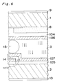
- Fig. 6 shows a schematic and sectional view of a liquid crystal display panel of Embodiment 2, while Table 3 shows the index of refraction and film thickness of each film in the liquid crystal display panel.
- this liquid crystal display panel is similar to that of Embodiment 1 shown in Fig. 4, except that the intermediate layers 12 and 13 are not formed.
- a common electrode made of color filters 8 and an indium tin oxide (ITO) film 104 is formed on a transparent top substrate 1 made of glass.
- an alignment film 106 made of polyimide is applied further to the ITO film 104.
- ITO films 105 for pixel electrodes connected to thin film transistors are formed on the thin film transistors 14 and SiN x films 111 are formed on a bottom substrate 2.
- the SiN x films 111 are not provided in the transmission part so as to make the ITO films 105 contact with an alignment film 107 there.
- the alignment film 107 made of a polyimide is formed on the ITO films 105 and the thin film transistors 14.
- a liquid crystal layer 3 is interposed between two layers of the alignment films 106, 107. That is, the ITO film 104 is formed directly on the color filters 8 and on the top substrate 1, while the ITO film 105 is formed directly on the bottom substrate 2.
- the difference of the index of refraction is 0.5 at an interface between the bottom substrate 2 and the ITO film 105 and it is also 0.5 at an interface between the top substrate 1 and the ITO film 104 formed on the top substrate 1 in non-transmission part.
- the film thicknesses "d" of the ITO films 104, 105 for the top and bottom substrates 1, 2 are set to be 140 nm, so that optical path length "nd" becomes 280 nm because the index "n" of refraction of the ITO films is 2.0.
- the above-mentioned relation (1) holds for the two ITO films 104, 105 if "i" is taken to be 1.
- Fig. 7 shows a graph of a spectrum of the liquid crystal display panel of Embodiment 2.
- the oscillation amplitude of the waveform of 10 - 15 nm of period is small, compared with Fig. 2, and this shows that the optical interference is not strong.
- the back light of a fluorescent lamp of three wavelengths type is transmitted through the liquid crystal display panel, no interference pattern and no change of hue are observed. That is, the quality of display is good.
- the optical path length "nd" of a single layer is determined to have a half or the like of the wavelength of green, to suppress the reflection of light in a wavelength range which can be recognized most easily even if the reflection at an interface is large.
- this concept can be applied not only to a single layer, but also to a multi-layer made of a plurality of adjacent layers.
- a liquid crystal display panel of Embodiment 3 of the invention shows one of such cases.
- Fig. 8 shows a sectional view of a liquid crystal display panel of Embodiment 3, while Table 4 shows the index of refraction and film thickness of each film in the liquid crystal display panel.
- This liquid crystal display panel is similar to that of Embodiment 2 shown in Fig. 5 mainly except that a SiN x film 211 as a transparent insulating film is formed on the ITO film 605 in the transmission part of the panel. That is, indium-tin-oxide (ITO) films 105 and thin film transistors 14 are formed on a bottom substrate 2, and SiN x films 211 as transparent insulating films are formed on the ITO films 105 to prevent the short circuit with the ITO film 104 for the top substrate 1. Then, an alignment film 207 is formed on the SiN x films 211 and thin film transistors 14.
- ITO indium-tin-oxide
- the film thickness "d" of the ITO film 105 for the bottom substrate 2 having 2.0 of index of refraction is set to be 140 nm, while that of the adjacent SiN x film 211 having 1.85 of index of refraction is set to be 190 nm.
- the total optical path length "nd" of a multi-layer consisting of the ITO films 105 and the SiN x films 211, or the sum of the optical path length of the two layers 105, 211 becomes 551.5 nm.
- the relation (1) when "i" 2 is satisfied. If the structure of the SiN x films 211 is compared with that of SiN x films 111 shown in Fig.
- the former SiN x layer 211 can also be taken as an intermediate layer introduced in Embodiment 1.
- the film thickness "d" of the ITO film 104 for the top substrate 1 is set to be 140 nm, so that optical path length "nd" of the layer 104 becomes 280 nm because the index "n” of refraction of the ITO films is 2.0.
- the relation (1) when "i" 1 is satisfied.
- Fig. 9 shows a graph of a spectrum of the liquid crystal display panel.
- the oscillation amplitude of the waveform has 10 - 15 nm of small period, and this shows that the optical interference is not so strong.
- the light of a fluorescent lamp of three wavelengths type as a back light is transmitted through the liquid crystal display panel, no interference pattern and no change of hue are observed. Thus, the quality of display is good.
- Table 4 Liquid crystal display panel of Embodiment 3 Kind of film Index of refraction Film thickness (nm) Glass substrate 1 1.5 1.1 * 106 Color filter 8 1.5 1500 ITO film 104 2.0 140 Alignment film 106 1.6 100 Liquid crystal 3 1.5 5000 Alignment film 207 1.6 100 SiN x 211 1.85 190 ITO film 105 2.0 100 Glass substrate 2 1.5 1.1*106
- the unevenness at the interface is suitable to be 0.01 - 0.5 ⁇ m in order to diffuse, scatter or refract visible light. That is, the distance between peaks or between bottoms of the uneven surface at the interface is preferably to be 0.01 - 0.5 ⁇ m as mentioned above.
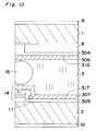
- FIG. 10 shows a sectional view of a liquid crystal display panel of Embodiment 4, while Table 5 shows the index of refraction and film thickness of each film in the liquid crystal display panel.
- the structure of the liquid crystal display panel is similar to that of Embodiment 2 mainly except rough interfaces 316, 317.
- SiN x films 11 are not formed over a bottom substrate 2 in a transmission part. Unevenness of about 0.1 ⁇ m is formed at the interface 317 between an ITO film 305 and an alignment film 307 and similar unevenness of about 0.1 ⁇ m is formed at the interface 316 between an ITO film 304 and an alignment film 306.
- the unevenness can be formed by controlling the crystal growth conditions of ITO films 304, 305 to increase the sizes of crystal grains of the ITO films. It can also be formed by etching the surface of the ITO films slightly or by using a technique such as shot peening.
- Table 5 Liquid crystal display panel of Embodiment 4 Kind of film Index of refraction Film thickness (nm) Glass substrate 1 1.5 1.1 * 106 Color filter 8 1.5 1500 ITO film 304 2.0 140 Alignment film 306 1.6 100 Liquid crystal 3 1.5 5000 Alignment film 307 1.6 100 ITO film 305 2.0 100 Glass substrate 2 1.5 1.1*106
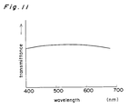
- Fig. 11 shows a graph of a spectrum of the liquid crystal display panel of Embodiment 4.
- the oscillation amplitude of the waveform has a very small period of 10 - 15 nm, and this shows that the optical interference is not so strong.
- the light of a fluorescent lamp of three wavelengths type as a back light is transmitted through the liquid crystal display panel, no interference pattern and no change of hue are observed and the quality of display is good when the liquid crystal display panel is observed both in a direction normal to the surface and in an oblique direction.
- the rough surfaces are formed over top and bottom substrates in this panel, it may be formed over only one of the two substrates. A similar good result can be obtained.
- Table 6 Liquid crystal display panel of Embodiment 4 Kind of film Index of refraction Film thickness (nm) Glass substrate 1 1.5 1.1 * 106 Color filter 8 1.5 1500 ITO film 404 2.0 50 Alignment film 406 1.6 100 Liquid crystal 3 1.5 5000 Alignment film 407 1.6 100 SiN x 411 1.85 100 ITO film 405 2.0 80 Glass substrate 2 1.5 1.1*106
- a minute uneven surface of 0.01 - 0.5 ⁇ m of unevenness formed in Embodiment 4 can also be formed at a surface of one of the layers provided between the top and bottom substrates.
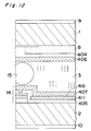
- Fig. 12 shows a sectional view of a liquid crystal display panel of Embodiment 5, while Table 6 shows the index of refraction and film thickness of each film in the liquid crystal display panel.
- the liquid crystal display panel has a structure similar to that of Embodiment 2 (Fig.
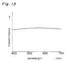
- Fig. 13 shows a graph of a spectrum of the liquid crystal display panel of Embodiment 5.
- the oscillation amplitude of the waveform has a small period of 10 - 15 nm, and this shows that the optical interference is not so strong.
- the light of a fluorescent lamp of three wavelengths type as a back light is transmitted through the liquid crystal display panel, no interference pattern and no change of hue are observed.
- the quality of display is good when the liquid crystal display panel is observed both in a direction normal to the surface and in an oblique direction.
- a rough surface is provided at the top surface of the SiN x films 411 in Embodiment 5, such a rough surface can also be provided at a different layer such as an electrode film (ITO film). Then, an alignment film can be formed on the rough surface.
- ITO film electrode film
- this invention can also be applied to a liquid crystal display panel of passive matrix type.
- this invention decreases the effect of the large difference of the index of refraction between adjacent films by decreasing the difference, by optimizing the film thickness or the index of refraction or by providing a rough interface.
- a change of hue due to the difference of the thicknesses of a film and of the liquid crystal layer can be suppressed, and an interference pattern due to the films and liquid crystal layer can be vanished. Then, a liquid crystal display panel of high quality can be produced at a high yield.
Landscapes
- Physics & Mathematics (AREA)
- Nonlinear Science (AREA)
- Mathematical Physics (AREA)
- Chemical & Material Sciences (AREA)
- Crystallography & Structural Chemistry (AREA)
- General Physics & Mathematics (AREA)
- Optics & Photonics (AREA)
- Liquid Crystal (AREA)
Applications Claiming Priority (2)
| Application Number | Priority Date | Filing Date | Title |
|---|---|---|---|
| JP345927/92 | 1992-12-25 | ||
| JP4345927A JPH06194639A (ja) | 1992-12-25 | 1992-12-25 | 液晶表示パネル |
Publications (2)
| Publication Number | Publication Date |
|---|---|
| EP0604903A2 true EP0604903A2 (de) | 1994-07-06 |
| EP0604903A3 EP0604903A3 (de) | 1995-04-12 |
Family
ID=18379943
Family Applications (1)
| Application Number | Title | Priority Date | Filing Date |
|---|---|---|---|
| EP93120769A Withdrawn EP0604903A3 (de) | 1992-12-25 | 1993-12-23 | Flüssigkristall-Anzeigetafel. |
Country Status (3)
| Country | Link |
|---|---|
| EP (1) | EP0604903A3 (de) |
| JP (1) | JPH06194639A (de) |
| KR (1) | KR940015631A (de) |
Cited By (4)
| Publication number | Priority date | Publication date | Assignee | Title |
|---|---|---|---|---|
| WO2002046836A3 (en) * | 2000-12-06 | 2003-01-16 | Optiva Inc | Liquid crystal information displays |
| WO2003040819A1 (en) * | 2001-11-09 | 2003-05-15 | Koninklijke Philips Electronics N.V. | Fast fast liquid crystal display system with high contrast |
| US7132138B2 (en) | 2000-12-06 | 2006-11-07 | Nitto Denko Corporation | Liquid crystal information displays |
| EP2433273A4 (de) * | 2009-05-22 | 2013-08-07 | Sharp Kk | Optische struktur zur reduzierung interner reflexionen und verfahren dafür |
Families Citing this family (24)
| Publication number | Priority date | Publication date | Assignee | Title |
|---|---|---|---|---|
| US6636757B1 (en) | 2001-06-04 | 2003-10-21 | Surgical Navigation Technologies, Inc. | Method and apparatus for electromagnetic navigation of a surgical probe near a metal object |
| US7998062B2 (en) | 2004-03-29 | 2011-08-16 | Superdimension, Ltd. | Endoscope structures and techniques for navigating to a target in branched structure |
| EP2316328B1 (de) | 2003-09-15 | 2012-05-09 | Super Dimension Ltd. | Umhüllungsvorrichtung zur Fixierung von Bronchoskopen |
| ATE438335T1 (de) | 2003-09-15 | 2009-08-15 | Super Dimension Ltd | System aus zubehör zur verwendung mit bronchoskopen |
| US8905920B2 (en) | 2007-09-27 | 2014-12-09 | Covidien Lp | Bronchoscope adapter and method |
| US9575140B2 (en) | 2008-04-03 | 2017-02-21 | Covidien Lp | Magnetic interference detection system and method |
| US8473032B2 (en) | 2008-06-03 | 2013-06-25 | Superdimension, Ltd. | Feature-based registration method |
| US8218847B2 (en) | 2008-06-06 | 2012-07-10 | Superdimension, Ltd. | Hybrid registration method |
| US8932207B2 (en) | 2008-07-10 | 2015-01-13 | Covidien Lp | Integrated multi-functional endoscopic tool |
| US8611984B2 (en) | 2009-04-08 | 2013-12-17 | Covidien Lp | Locatable catheter |
| US10582834B2 (en) | 2010-06-15 | 2020-03-10 | Covidien Lp | Locatable expandable working channel and method |
| US10952593B2 (en) | 2014-06-10 | 2021-03-23 | Covidien Lp | Bronchoscope adapter |
| US10426555B2 (en) | 2015-06-03 | 2019-10-01 | Covidien Lp | Medical instrument with sensor for use in a system and method for electromagnetic navigation |
| US10478254B2 (en) | 2016-05-16 | 2019-11-19 | Covidien Lp | System and method to access lung tissue |
| US10418705B2 (en) | 2016-10-28 | 2019-09-17 | Covidien Lp | Electromagnetic navigation antenna assembly and electromagnetic navigation system including the same |
| US10722311B2 (en) | 2016-10-28 | 2020-07-28 | Covidien Lp | System and method for identifying a location and/or an orientation of an electromagnetic sensor based on a map |
| US10792106B2 (en) | 2016-10-28 | 2020-10-06 | Covidien Lp | System for calibrating an electromagnetic navigation system |
| US10751126B2 (en) | 2016-10-28 | 2020-08-25 | Covidien Lp | System and method for generating a map for electromagnetic navigation |
| US10638952B2 (en) | 2016-10-28 | 2020-05-05 | Covidien Lp | Methods, systems, and computer-readable media for calibrating an electromagnetic navigation system |
| US10446931B2 (en) | 2016-10-28 | 2019-10-15 | Covidien Lp | Electromagnetic navigation antenna assembly and electromagnetic navigation system including the same |
| US10517505B2 (en) | 2016-10-28 | 2019-12-31 | Covidien Lp | Systems, methods, and computer-readable media for optimizing an electromagnetic navigation system |
| US10615500B2 (en) | 2016-10-28 | 2020-04-07 | Covidien Lp | System and method for designing electromagnetic navigation antenna assemblies |
| US11219489B2 (en) | 2017-10-31 | 2022-01-11 | Covidien Lp | Devices and systems for providing sensors in parallel with medical tools |
| US12089902B2 (en) | 2019-07-30 | 2024-09-17 | Coviden Lp | Cone beam and 3D fluoroscope lung navigation |
Family Cites Families (4)
| Publication number | Priority date | Publication date | Assignee | Title |
|---|---|---|---|---|
| JPS5389450A (en) * | 1977-01-17 | 1978-08-07 | Seiko Epson Corp | Digital watch |
| US4895432A (en) * | 1985-01-30 | 1990-01-23 | Seiko Epson Corporation, A Japanese Corporation | Display device having anti-reflective electrodes and/or insulating film |
| JPH03142417A (ja) * | 1989-10-30 | 1991-06-18 | Sharp Corp | カラー液晶ディスプレイ |
| JPH03209223A (ja) * | 1990-01-12 | 1991-09-12 | Hitachi Ltd | 液晶表示装置 |
-
1992
- 1992-12-25 JP JP4345927A patent/JPH06194639A/ja active Pending
-
1993
- 1993-12-23 EP EP93120769A patent/EP0604903A3/de not_active Withdrawn
- 1993-12-23 KR KR1019930029195A patent/KR940015631A/ko not_active Ceased
Cited By (5)
| Publication number | Priority date | Publication date | Assignee | Title |
|---|---|---|---|---|
| WO2002046836A3 (en) * | 2000-12-06 | 2003-01-16 | Optiva Inc | Liquid crystal information displays |
| US7132138B2 (en) | 2000-12-06 | 2006-11-07 | Nitto Denko Corporation | Liquid crystal information displays |
| WO2003040819A1 (en) * | 2001-11-09 | 2003-05-15 | Koninklijke Philips Electronics N.V. | Fast fast liquid crystal display system with high contrast |
| US6914654B2 (en) | 2001-11-09 | 2005-07-05 | Koninklijke Philips Electronics N.V. | High contrast fast liquid crystal display system |
| EP2433273A4 (de) * | 2009-05-22 | 2013-08-07 | Sharp Kk | Optische struktur zur reduzierung interner reflexionen und verfahren dafür |
Also Published As
| Publication number | Publication date |
|---|---|
| KR940015631A (ko) | 1994-07-21 |
| JPH06194639A (ja) | 1994-07-15 |
| EP0604903A3 (de) | 1995-04-12 |
Similar Documents
| Publication | Publication Date | Title |
|---|---|---|
| EP0604903A2 (de) | Flüssigkristall-Anzeigetafel | |
| KR102708316B1 (ko) | 표시 장치 | |
| US8179504B2 (en) | Liquid crystal display with a light selective reflection filter | |
| KR101256545B1 (ko) | 횡전계 모드 반사투과형 액정표시장치 | |
| KR101220479B1 (ko) | 광학 필터, 액정 패널 및 액정 표시 장치 | |
| US7486355B2 (en) | Color filter panel and liquid crystal display including the same | |
| US7952658B2 (en) | IPS LCD device having a wider viewing angle | |
| US7388635B2 (en) | Liquid crystal display device and display equipment using the same | |
| KR102115564B1 (ko) | 표시기판 및 이를 포함하는 표시패널 | |
| KR100371758B1 (ko) | 액정표시장치 | |
| US8218108B2 (en) | Liquid crystal display panel and liquid crystal display device | |
| KR20050043678A (ko) | 조명 장치 및 이를 포함하는 디스플레이 장치 | |
| US7855775B2 (en) | Liquid crystal display device | |
| JPH06331975A (ja) | カラー液晶ディスプレイ | |
| KR20240082212A (ko) | 디스플레이 모듈 | |
| US20090184622A1 (en) | Lamp and display device having the same | |
| US7212342B2 (en) | Structure of a color filter | |
| US12080719B2 (en) | Display panel and display device | |
| US20060187389A1 (en) | Liquid crystal display device | |
| KR100600931B1 (ko) | 컬러필터 구조체 | |
| JP4098753B2 (ja) | カラーフィルタの構造 | |
| KR100310697B1 (ko) | 반사형 칼라 액정 표시소자 | |
| JPH1195198A (ja) | 液晶表示装置 | |
| JPH02256022A (ja) | 液晶表示パネルの光源とそれを用いた液晶表示装置 | |
| KR20060022884A (ko) | 액정 디스플레이 패널 |
Legal Events
| Date | Code | Title | Description |
|---|---|---|---|
| PUAI | Public reference made under article 153(3) epc to a published international application that has entered the european phase |
Free format text: ORIGINAL CODE: 0009012 |
|
| 17P | Request for examination filed |
Effective date: 19931223 |
|
| AK | Designated contracting states |
Kind code of ref document: A2 Designated state(s): DE FR GB |
|
| PUAL | Search report despatched |
Free format text: ORIGINAL CODE: 0009013 |
|
| AK | Designated contracting states |
Kind code of ref document: A3 Designated state(s): DE FR GB |
|
| 17Q | First examination report despatched |
Effective date: 19970702 |
|
| STAA | Information on the status of an ep patent application or granted ep patent |
Free format text: STATUS: THE APPLICATION HAS BEEN WITHDRAWN |
|
| 18W | Application withdrawn |
Withdrawal date: 19971031 |