EP0604965B1 - Halbleiterlaser mit Begrenzungsschicht aus AlGaInP - Google Patents
Halbleiterlaser mit Begrenzungsschicht aus AlGaInP Download PDFInfo
- Publication number
- EP0604965B1 EP0604965B1 EP93120981A EP93120981A EP0604965B1 EP 0604965 B1 EP0604965 B1 EP 0604965B1 EP 93120981 A EP93120981 A EP 93120981A EP 93120981 A EP93120981 A EP 93120981A EP 0604965 B1 EP0604965 B1 EP 0604965B1
- Authority
- EP
- European Patent Office
- Prior art keywords
- layer
- semiconductor laser
- cladding layer
- light diffusion
- proportion
- Prior art date
- Legal status (The legal status is an assumption and is not a legal conclusion. Google has not performed a legal analysis and makes no representation as to the accuracy of the status listed.)
- Expired - Lifetime
Links
Images


Classifications
-
- H—ELECTRICITY
- H01—ELECTRIC ELEMENTS
- H01S—DEVICES USING THE PROCESS OF LIGHT AMPLIFICATION BY STIMULATED EMISSION OF RADIATION [LASER] TO AMPLIFY OR GENERATE LIGHT; DEVICES USING STIMULATED EMISSION OF ELECTROMAGNETIC RADIATION IN WAVE RANGES OTHER THAN OPTICAL
- H01S5/00—Semiconductor lasers
- H01S5/30—Structure or shape of the active region; Materials used for the active region
- H01S5/34—Structure or shape of the active region; Materials used for the active region comprising quantum well or superlattice structures, e.g. single quantum well [SQW] lasers, multiple quantum well [MQW] lasers or graded index separate confinement heterostructure [GRINSCH] lasers
- H01S5/343—Structure or shape of the active region; Materials used for the active region comprising quantum well or superlattice structures, e.g. single quantum well [SQW] lasers, multiple quantum well [MQW] lasers or graded index separate confinement heterostructure [GRINSCH] lasers in AIIIBV compounds, e.g. AlGaAs-laser, InP-based laser
- H01S5/34313—Structure or shape of the active region; Materials used for the active region comprising quantum well or superlattice structures, e.g. single quantum well [SQW] lasers, multiple quantum well [MQW] lasers or graded index separate confinement heterostructure [GRINSCH] lasers in AIIIBV compounds, e.g. AlGaAs-laser, InP-based laser with a well layer having only As as V-compound, e.g. AlGaAs, InGaAs
-
- B—PERFORMING OPERATIONS; TRANSPORTING
- B82—NANOTECHNOLOGY
- B82Y—SPECIFIC USES OR APPLICATIONS OF NANOSTRUCTURES; MEASUREMENT OR ANALYSIS OF NANOSTRUCTURES; MANUFACTURE OR TREATMENT OF NANOSTRUCTURES
- B82Y20/00—Nanooptics, e.g. quantum optics or photonic crystals
-
- H—ELECTRICITY
- H01—ELECTRIC ELEMENTS
- H01S—DEVICES USING THE PROCESS OF LIGHT AMPLIFICATION BY STIMULATED EMISSION OF RADIATION [LASER] TO AMPLIFY OR GENERATE LIGHT; DEVICES USING STIMULATED EMISSION OF ELECTROMAGNETIC RADIATION IN WAVE RANGES OTHER THAN OPTICAL
- H01S5/00—Semiconductor lasers
- H01S5/20—Structure or shape of the semiconductor body to guide the optical wave ; Confining structures perpendicular to the optical axis, e.g. index or gain guiding, stripe geometry, broad area lasers, gain tailoring, transverse or lateral reflectors, special cladding structures, MQW barrier reflection layers
- H01S5/22—Structure or shape of the semiconductor body to guide the optical wave ; Confining structures perpendicular to the optical axis, e.g. index or gain guiding, stripe geometry, broad area lasers, gain tailoring, transverse or lateral reflectors, special cladding structures, MQW barrier reflection layers having a ridge or stripe structure
- H01S5/223—Buried stripe structure
- H01S5/2231—Buried stripe structure with inner confining structure only between the active layer and the upper electrode
-
- H—ELECTRICITY
- H01—ELECTRIC ELEMENTS
- H01S—DEVICES USING THE PROCESS OF LIGHT AMPLIFICATION BY STIMULATED EMISSION OF RADIATION [LASER] TO AMPLIFY OR GENERATE LIGHT; DEVICES USING STIMULATED EMISSION OF ELECTROMAGNETIC RADIATION IN WAVE RANGES OTHER THAN OPTICAL
- H01S5/00—Semiconductor lasers
- H01S5/20—Structure or shape of the semiconductor body to guide the optical wave ; Confining structures perpendicular to the optical axis, e.g. index or gain guiding, stripe geometry, broad area lasers, gain tailoring, transverse or lateral reflectors, special cladding structures, MQW barrier reflection layers
- H01S5/22—Structure or shape of the semiconductor body to guide the optical wave ; Confining structures perpendicular to the optical axis, e.g. index or gain guiding, stripe geometry, broad area lasers, gain tailoring, transverse or lateral reflectors, special cladding structures, MQW barrier reflection layers having a ridge or stripe structure
- H01S5/2205—Structure or shape of the semiconductor body to guide the optical wave ; Confining structures perpendicular to the optical axis, e.g. index or gain guiding, stripe geometry, broad area lasers, gain tailoring, transverse or lateral reflectors, special cladding structures, MQW barrier reflection layers having a ridge or stripe structure comprising special burying or current confinement layers
- H01S5/2206—Structure or shape of the semiconductor body to guide the optical wave ; Confining structures perpendicular to the optical axis, e.g. index or gain guiding, stripe geometry, broad area lasers, gain tailoring, transverse or lateral reflectors, special cladding structures, MQW barrier reflection layers having a ridge or stripe structure comprising special burying or current confinement layers based on III-V materials
- H01S5/2209—GaInP based
-
- H—ELECTRICITY
- H01—ELECTRIC ELEMENTS
- H01S—DEVICES USING THE PROCESS OF LIGHT AMPLIFICATION BY STIMULATED EMISSION OF RADIATION [LASER] TO AMPLIFY OR GENERATE LIGHT; DEVICES USING STIMULATED EMISSION OF ELECTROMAGNETIC RADIATION IN WAVE RANGES OTHER THAN OPTICAL
- H01S5/00—Semiconductor lasers
- H01S5/30—Structure or shape of the active region; Materials used for the active region
- H01S5/32—Structure or shape of the active region; Materials used for the active region comprising PN junctions, e.g. hetero- or double- heterostructures
- H01S5/3211—Structure or shape of the active region; Materials used for the active region comprising PN junctions, e.g. hetero- or double- heterostructures characterised by special cladding layers, e.g. details on band-discontinuities
Definitions
- the present invention relates to a semiconductor laser usable for pumping an Er-doped quartz optical fiber amplifier and other purposes.
- the invention also relates to a stripe-type semiconductor laser having a GaAs substrate.
- An Er-doped quartz optical fiber amplifier now attracts much attention as one of kernel devices and technologies of next generation optical communication systems.
- a semiconductor laser having a wavelength of 1.48 ⁇ m or 0.98 ⁇ m is used as a pumping light source for that optical amplifier.
- a 0.98- ⁇ m semiconductor laser which has a GaInAs quantum well active layer and AlGaAs or GaInP cladding layers.
- a quantum well active layer and optical confinement layers need to be made thinner.
- the thinning of the quantum well active layer and optical confinement layers deteriorates the optical confinement efficiency.
- carriers are confined insufficiently, to deteriorate temperature characteristics. Due to the above phenomena inherent in a semiconductor laser, the above-mentioned 0.98- ⁇ m semiconductor laser cannot satisfy both of high output power and superior temperature characteristics required for a pumping light source for the Er-doped quartz optical fiber amplifier.
- semiconductor lasers are now being developed in which light and current are confined by a structure made of only semiconductors.
- the energy of oscillation light is greater than or equal to the band gap energy of GaAs
- light can be substantially confined by forming a mesa portion (protrusion strip) in a clad and filling the side regions of the mesa portion with GaAs, where the side portions serve to absorb guided light.
- this type of structure cannot be employed in 1- ⁇ m-band semiconductor lasers, various attempts have been made in those semiconductor lasers.
- a technique of filling the side regions of a clad mesa portion with a material whose effective refractive index is smaller than the clad is now being investigated actively, because this type of structure can be produced relatively easily.
- a clad is made of AlGaAs and the side regions of a meas portion is filled with GaInP whose refractive index is smaller than AlGaAs (Chida et al., The 40th Spring Conference of the Japan Society of Applied Physics, Presentation No. 1a-C-2 (1993)).
- a mesa portion including a high-refractivity GaAs layer is formed in a clad made of GaInP, and the side regions of the GaAs layer is filled with GaInP (Sagawa et al., The 40th Spring Conference of the Japan Society of Applied Physics, Presentation No. 31p-C-11 (1993)).
- the above two techniques employ the real refractive index waveguide structure, in which the side regions of a mesa portion are filled with a low-refractivity material.
- a red semiconductor laser of an index antiguiding structure has been proposed in which the side regions of a mesa portion of an AlGaInP clad are filled with AlGaInP of a smaller Al proportion (Kidoguchi et al., The Autumn Conference of the Japan Society of Applied Physics, Presentation No. 18a-V-5 (1992)). Since this index antiguiding structure can produce a large difference between thresholds of the fundamental transverse mode and higher order transverse modes, it can readily provide a single transverse mode operation.
- the first conventional technique of Chida et al. has a problem of a small control range of optical confinement, because the clad material is limited to AlGaAs whose refractive index is larger than GaInP as the embedding material.
- the second conventional technique of Sagawa et al. the increase of the refractive index difference in the horizontal direction will necessarily be associated with excessive concentration of light in the GaAs layer.
- Kidoguchi et al. having the index antiguiding structure can readily provide a single transverse mode operation, it requires the AlGaInP light diffusion layer (which buries the mesa portion (protrusion strip)) to have a small Al proportion (Ga/(Al + Ga)) of 0.6. It is difficult to control growth conditions and pre-treatment conditions of the growth of the AlGaInP light diffusion layer. That is, since the quantum well active layer of the semiconductor laser of Kidoguchi et al. is made of GaInP, whose band gap energy is much larger than GaAs, the Al proportion of the clad needs to be increased to effectively confine carriers, necessitating the increase of the Al proportion of the light diffusion layer.
- An object of the present invention is to provide a semiconductor laser having high output power and superior temperature characteristics specifically suitable for use as a pumping light source for an Er-doped optical fiber amplifier.
- One special embodiment of the invention provides an index antiguiding type semiconductor laser which can confine light and current by a structure made of only semiconductor materials and can easily provide a single transverse mode operation, and which can control optical confinement in both of the vertical and horizontal directions.
- a carrier (electron) overflow from the active region to the p-type cladding layer is the main factor of a loss occurring in high-current injection.
- it is effective to increase a barrier height between the quantum well active layer and the cladding layer (i.e., a conduction band discontinuity between GaInAs and AlGaInP).
- a conduction band discontinuity between GaInAs and AlGaInP.
- the conduction band discontinuity is approximately twice that of GaInP.
- AlGaInP (including the case where the Al proportion is zero) of the light diffusion layer has a refractive index larger than that of AlGaInP of the protrusion strip, light tends to diffuse in the horizontal direction. However, because of a gain obtained under the protrusion strip, the light is substantially concentrated in the central region to attain light guidance. Since the degree of light diffusion in the horizontal direction varies with the mode, the transverse mode can be controlled by adjusting the refractive index of the protrusion strip. If the Al proportion (Al/(Al + Ga)) of AlGaInP of the protrusion strip is increased (i.e., the refractive index is decreased) to provide a higher degree of diffusion, the gain becomes insufficient for light guidance.
- the light diffusion layer is epitaxially grown from the surface produced by shaping the protrusion strip and is therefore exposed to air, it is difficult to restart growth of AlGaInP.
- the quantum well active layer is made of a material, for instance, GaInAs, whose band gap energy is smaller than that of GaAs, the Al proportion of AlGaInP of the light diffusion layer can be made sufficiently small. The growth of AlGaInP can be restarted more easily if its Al proportion is smaller. In view of this, it is preferred that the Al proportion of AlGaInP of the light diffusion layer not exceed 0.2.
- Restarting of the AlGaInP growth of the light diffusion layer is further facilitated by forming, in advance, at least one of a GaAs and GaAsP thin layers which include only one group III element. It is preferred that these layers have a total thickness less than about 50 ⁇ , because if they are too thick the optical confinement in the horizontal direction is deteriorated. Where GaInP is used (that is, the Al proportion of AlGaInP is zero) for the light diffusion layer, it can be grown more easily.
- the light distribution in the vertical direction can be controlled by changing the composition and thickness of AlGaInP of the base layer of the top clad which AlGaInP has an Al proportion larger than that of the protrusion strip. Further, if the longitudinal ends of the protrusion strip are spaced from the laser facets and the light diffusion layer is extended to fill the regions in between, the light expands in the facet portions to reduce the light density there and, therefore, the deterioration of the laser facets can be suppressed.
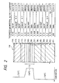
- Fig. 1 schematically shows a vertical structure of a semiconductor laser which is not an embodiment of the present invention.
- Respective epitaxial layers 2-16 are formed on an n-type GaAs substrate 1 by a known metal organic vapor phase epitaxy (MOVPE). Materials and thicknesses of the respective epitaxial layers 2-16 are as follows.
- Reference numerals 17 and 18 denote a p-side electrode and an n-side electrode, respectively.
- the values x of the AlGaInP layers 3, 4, 10, 11, 13 and 14 are composition ratios of Al to (Al + Ga).
- AlGaInP of the respective layers is substantially lattice-matched with GaAs.
- the AlGaInP layers 3, 4, 10, 11, 13 and 14 be grown at temperatures about 50°C higher than the GaInP layers.
- the n-type AlGaInP layer 3 is grown at 760°C
- the p-type AlGaInP layers 11, 13 and 14 are grown at 740°C.
- the flow rate of diethylzinc which is a material gas of Zn as the p-type dopant, is set at the same level as in the case of forming the Zn-doped GaAs contact layer 15.
- this semiconductor laser since GaInAs is used for the quantum well active layer and AlGaInP is used for the cladding layers, a large difference can be obtained between the band gap energies of the quantum well active layer and the cladding layers. As a result, a large electron energy level difference is produced, and electrons are less likely to escape from the quantum well active layer, which means that the electron-hole recombination is effectively performed in the quantum well active layer.
- this semiconductor laser can produce a sufficiently high output power suitable for a pumping light source for an Er-doped quartz optical fiber amplifier without deteriorating temperature characteristics.
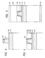
- an epitaxial wafer 116 having a multilayered structure of Fig. 2 is formed by a reduced pressure MOVPE at about 60 Torr.
- An n-type GaAs buffer layer 102, an n-type AlGaInP cladding layer 103, an active region 115, a p-type AlGaInP cladding layer 111, a p-type GaInP etching stopper layer 112, a p-type AlGaInP cladding layer 113 and a p-type GaInP cap layer 114 are sequentially formed on a GaAs substrate 101 by epitaxial growth.
- the active region 115 consists of a GaInP cladding layer 104, a GaInAsP optical confinement layer 105, a GaAs layer 106, a GaInAs quantum well layer 107, a GaAs layer 108, a GaInAsP optical confinement layer 109 and a GaInP cladding layer 110.
- the p-type AlGaInP cladding layer 111, p-type GaInP etching stopper layer 112, p-type AlGaInP cladding layer 113 and p-type GaInP cap layer constitutes a top clad.
- the p-type AlGaInP cladding layer 113 is shaped, by subsequent etching, into a protrusion strip that is coextensive and parallel with a current-injecting portion of the quantum well active layer.
- Thicknesses, kinds and concentrations of dopants of the respective epitaxial layers are indicated in Fig. 2. Also shown in the left part of Fig. 2 is a variation of the temperature during the epitaxial growth. It is desired that AlGaInP for the clads be grown at a higher temperature, and that GaInAs for the quantum well active layer be grown at a lower temperature. In this embodiment, as shown in Fig. 2, the active region 115 is grown at 650°C and the bottom and top clads are grown at 720-740°C.
- GaInP cap layer 114 and the AlGaInP cladding layer 113 of the thus formed epitaxial wafer 116 are removed by etching.
- a 0.1- ⁇ m-thick silicon nitride film is deposited on the entire surface, and patterned by a lithography technique to leave a 4- ⁇ m-wide bandlike portion 120.
- the GaInP cap layer 114 and the AlGaInP cladding layer 113 are etched using the silicon nitride film 120 as a mask (see Fig. 3).
- the GaInP cap layer 114 and a very surface portion of the AlGaInP cladding layer 113 are etched out by a mixture at 50°C of sulfuric acid, hydrogen peroxide and water which are mixed at a ratio of 3:1:1.
- the AlGaInP cladding layer 113 is etched by concentrated sulfuric acid of 60°C until the color of the wafer surface changes, which means exposure of the GaInP etching stopper layer 112.
- a protrusion strip 121 of the top clad is formed as shown in Fig. 3.
- a light diffusion layer 132 of n-type GaInP is formed so as to occupy both sides of the protrusion strip 121.
- a GaAs layer 130 and a GaAsP layer 131 are formed prior to the formation of the light diffusion layer 132.
- the wafer surface is rough at the time of restarting growth of the light diffusion layer 132.
- the surface condition is bad, i.e., not suitable for the growth of the light-diffusion layer 132.
- the GaAs layer 130 and the GaAsP layer 131 serve to facilitate the growth of the light diffusion layer 132.
- the total thickness of the layers 130 and 131 should be less than about 50 ⁇ , because if they are two thick, they will adversely affect the optical confinement in the horizontal direction.
- the GaAs layer 130 is 30- ⁇ thick and the GaAsP layer 131 is 10- ⁇ thick.
- the composition of the GaAsP layer 130 need not be selected strictly.
- the mole ratio between arsine and phosphine may be set at about 0.1 and the mole ratio between the group V elements and the group III element may be set at about 70.
- the temperature should be raised in a phosphine atmosphere.
- the light diffusion layer 132 also serves as a current blocking layer.
- the silicon nitride film 120 is etched out by a solution of hydrofluoric acid and water (1:1), and a p-type GaAs film 140 is formed to have a thickness of 2 ⁇ m.
- a p-side electrode 141 is evaporated onto the p-type GaAs film 140.
- an n-side electrode 142 is evaporated onto it.
- the electrodes 141 and 142 are alloyed with the adjacent layers by annealing, cleaving and mounting steps are performed to complete a semiconductor laser (see Fig. 5).
- the optical confinement in both of the vertical and horizontal directions can be controlled by changing the thickness and composition (distribution) of a base layer of the top clad, i.e., the AlGaInP cladding layer 111 in this embodiment.
- a base layer of the top clad i.e., the AlGaInP cladding layer 111 in this embodiment.
- the mesa shape of the protrusion strip 121 is an ordinary one (the top is narrower than the bottom), it may be a reversed one, in which case the stripe width can be reduced.
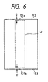
- Fig. 6 is a top view corresponding to Fig. 5, and shows how the protrusion strip 121 is arranged on a chip as cut out.
- ends 121a and 121b of the protrusion strip 121 are separated from facets 152 and 153.
- the light diffusion layer also fills the regions between the end 121a and the facet 152 and between the end 121b and the facet 153 in the same manner as in the lateral sides of the protrusion strip 121. It is preferred that distances d between the end 121a and facet 152 and between the end 121b and the facet 153 be about 20 ⁇ m.
- Base layers of the top clad i.e., the p-type AlGaInP cladding layer 111 and the p-type GaInP etching stopper layer 112 extend to the facets 152 and 153. Since the above facet structure causes light diffusion in the vicinity of the facets, the light density can be reduced there.
- a sudden failure may occur in semiconductor lasers having a GalnAs quantum well active layer.
- the sudden failure is caused by fusion of a facet, which is called a catastrophic optical damage (COD) and is considered as originating from an interaction between light and current at a facet portion. If the light density is reduced at the facet portions by using the facet structure of this embodiment, the COD will hardly occur to improve the reliability of the semiconductor laser.
- COD catastrophic optical damage
- the above structure is employed in both facet portions. Where coatings of different reflectances are applied to the respective facets, the above structure may be employed only for the lower-reflectance-side facet, in which case the protrusion strip 121 is extended to the facet on the higher reflectance side.
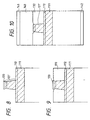
- Fig. 7 shows a multilayered structure of an epitaxial wafer to be used for producing a semiconductor laser according to a second embodiment of the invention.
- the second embodiment is different from the first embodiment in that the light diffusion layer uses, instead of GaInP, AlGaInP whose refractive index is larger than AlGaInP of the protrusion strip.
- the AlGaInP cladding layers 103 and 113 of the epitaxial wafer 116 of the first embodiment are replaced by AlGaInP layers 103' and 113' having a large Al proportion to constitute an epitaxial wafer 116'.
- the procedure of forming the epitaxial wafer 116' is basically the same as in the first embodiment.
- the temperature in forming the top clad is a little higher than in the first embodiment (see Fig. 7).
- a protrusion strip 121' is formed by etching as shown in Fig. 8, and then a light diffusion layer 170 is formed as shown in Fig. 9 which is made of n-type AlGaInP having an Al proportion (Al/(Al + Ga)) of 0.2.
- the light diffusion layer 170 is formed directly on the etching stopper layer 112, to facilitate the epitaxial growth the GaAs layer 130 and the GaAsP layer 131 may be formed in advance as in the case of the first embodiment.
- the p-type GaAs film 140 and the electrodes 141 and 142 are formed, and a chip is cut out to complete a semiconductor laser (see Fig. 10).
- Figs. 11-13 show epitaxial wafers according to third to fifth embodiments, which are alternatives to the epitaxial wafer 116 of Fig. 2.
- an etching stopper layer of GaAs is employed instead of the etching stopper layer 112 of GaInP of the first embodiment.
- This change provides larger selection ranges to contribute to stabilization of the manufacturing process.
- a room temperature solution of hydrochloric acid, phosphoric acid and water (22:11:17) may be used as an etchant.
- an n-side (top) clad and a p-side (bottom) clad are made approximately symmetrical. Even in the first embodiment, the light distributions on the n and p sides can be made identical by adjusting the thickness of the AlGaInP cladding layer 111 and other factors. It is apparent that the epitaxial wafer of the fourth embodiment can equalize the n-side and p-side light distributions more easily.
- the Al proportion (Al/(Al + Ga)) of a base layer of the top clad is set the same as that of a protrusion strip, to make the large part of the clad have the same composition. This will facilitate the epitaxial growth.
- the semiconductor lasers according to the first to fifth embodiments exhibit good heat dissipation performance because they confine light and current by a structure made of only semiconductor materials.
- the single transverse mode operation can easily be obtained by virtue of the index antiguiding structure.
Landscapes
- Physics & Mathematics (AREA)
- Optics & Photonics (AREA)
- Engineering & Computer Science (AREA)
- Electromagnetism (AREA)
- General Physics & Mathematics (AREA)
- Chemical & Material Sciences (AREA)
- Condensed Matter Physics & Semiconductors (AREA)
- Nanotechnology (AREA)
- Geometry (AREA)
- Life Sciences & Earth Sciences (AREA)
- Biophysics (AREA)
- Crystallography & Structural Chemistry (AREA)
- Semiconductor Lasers (AREA)
Claims (5)
- Ein Halbleiterlaser, der folgendes umfaßt:ein GaAs-Substrat;einen aktiven Bereich (115), der eine aktive Quantentrogschicht (7,107) umfaßt, die eine Bandlücke hat, die kleiner ist als die von GaAs; undeinen oberen Begrenzungsschichtbereich, der eine erste Begrenzungsschicht (111) vom p-Typ umfaßt, der auf dem aktiven Bereich (115) angeordnet ist und im wesentlichen gitterangepaßt mit dem GaAs-Substrat ist;dadurch gekennzeichnet, daßdie erste Begrenzungsschicht (111) aus
 der Halbleiterlaser weiterhin einen hervorstehenden Streifen (121) zur Stromeinkopplung umfaßt, der oberhalb der ersten Begrenzungsschicht (111) angeordnet ist und eine zweite Begrenzungsschicht (113) aus (AlyGa1-y)0,5In0,5P (O < y < x) umfaßt, die einen Al-Anteil y hat, der kleiner ist als der Al-Anteil x der ersten Begrenzungsschicht (111), undeine Lichtdiffusionsschicht (132) aus (AlzGa1-z)0,5In0,5P (O ≤ z < y), die auf der ersten Begrenzungsschicht (111) benachbart zu dem hervorstehenden Streifen (121) gebildet ist, wobei die Lichtdiffusionsschicht (132) einen Al-Anteil z hat, der kleiner ist als der Al-Anteil y der zweiten Begrenzungsschicht (113) und Null miteinschließt, umfaßt,wobei die erste Begrenzungsschicht (111) eine solche Dicke hat, daß das Licht der Laserschwingung in die Lichtdiffusionsschicht (132) entweichen kann, um einen Halbleiterlaser vom Index-antigeführten Typ zu bilden.
 - Ein Halbleiterlaser nach Anspruch 1, worin die Differenz zwischen dem Al-Anteil y der zweiten Begrenzungsschicht (113) und den Al-Anteil z der Lichtdiffusionsschicht im Bereich von 0,1 bis 0,4 ist.
- Ein Halbleiterlaser nach Anspruch 2, worin der Al-Anteil z der Lichtdiffusionsschicht (132) nicht größer als 0,2 ist.
- Ein Halbleiterlaser nach Anspruch 1, der weiterhin zumindest eine GaAs-Schicht (130) oder eine GaAsP-Schicht (131) zwischen der Lichtdiffusionsschicht (132) und der ersten Begrenzungsschicht (111) und zwischen der Lichtdiffusionsschicht (132) und dem hervorstehenden Streifen (121) umfaßt.
- Ein Halbleiterlaser nach Anspruch 1, worin die longitudinalen Endoberflächen (121a,121b) des hervorstehenden Streifens (121), welche parallel zu den Laserfacetten (152, 153) sind, von den jeweiligen Laserfacetten (152,153) beabstandet sind und die Lichtdiffusionsschicht (132) sich so erstreckt, daß sie die Bereiche zwischen den longitudinalen Endoberflächen (121a,121b) des hervorstehenden Streifens (121) und den Laserfacetten (152,153) ausfüllt.
Applications Claiming Priority (6)
| Application Number | Priority Date | Filing Date | Title |
|---|---|---|---|
| JP34928092A JPH06204613A (ja) | 1992-12-28 | 1992-12-28 | 半導体レーザ |
| JP349280/92 | 1992-12-28 | ||
| JP9438293 | 1993-04-21 | ||
| JP94382/93 | 1993-04-21 | ||
| JP18834193A JPH077230A (ja) | 1993-04-21 | 1993-07-29 | 屈折率反導波型半導体レーザ |
| JP188341/93 | 1993-07-29 |
Publications (2)
| Publication Number | Publication Date |
|---|---|
| EP0604965A1 EP0604965A1 (de) | 1994-07-06 |
| EP0604965B1 true EP0604965B1 (de) | 1997-09-10 |
Family
ID=27307531
Family Applications (1)
| Application Number | Title | Priority Date | Filing Date |
|---|---|---|---|
| EP93120981A Expired - Lifetime EP0604965B1 (de) | 1992-12-28 | 1993-12-27 | Halbleiterlaser mit Begrenzungsschicht aus AlGaInP |
Country Status (4)
| Country | Link |
|---|---|
| US (1) | US5586135A (de) |
| EP (1) | EP0604965B1 (de) |
| CA (1) | CA2112319C (de) |
| DE (1) | DE69313807T2 (de) |
Families Citing this family (6)
| Publication number | Priority date | Publication date | Assignee | Title |
|---|---|---|---|---|
| US5764671A (en) * | 1996-10-21 | 1998-06-09 | Motorola, Inc. | VCSEL with selective oxide transition regions |
| US6461884B1 (en) * | 2001-01-05 | 2002-10-08 | Manijeh Razeghi | Diode laser |
| JP2006245341A (ja) * | 2005-03-03 | 2006-09-14 | Mitsubishi Electric Corp | 半導体光素子 |
| JP2007250896A (ja) * | 2006-03-16 | 2007-09-27 | Sumitomo Electric Ind Ltd | 半導体光素子 |
| CN104757223B (zh) * | 2009-04-09 | 2019-12-10 | 福尔杰咖啡公司 | 咖啡片及其制备方法 |
| CN106384771B (zh) * | 2016-10-25 | 2019-01-11 | 华灿光电(浙江)有限公司 | AlGaInP基发光二极管外延片、芯片及制备方法 |
Family Cites Families (10)
| Publication number | Priority date | Publication date | Assignee | Title |
|---|---|---|---|---|
| JPH01181493A (ja) * | 1988-01-09 | 1989-07-19 | Sharp Corp | 端面窓型半導体レーザ素子 |
| GB2222307B (en) * | 1988-07-22 | 1992-04-01 | Mitsubishi Electric Corp | Semiconductor laser |
| US5146466A (en) * | 1988-09-29 | 1992-09-08 | Sanyo Electric Co., Ltd. | Semiconductor laser device |
| JP2978530B2 (ja) * | 1990-06-05 | 1999-11-15 | 富士通株式会社 | 半導体レーザ装置 |
| JPH04150087A (ja) * | 1990-10-12 | 1992-05-22 | Mitsubishi Electric Corp | 可視光半導体レーザ装置 |
| US5210767A (en) * | 1990-09-20 | 1993-05-11 | Mitsubishi Denki Kabushiki Kaisha | Semiconductor laser |
| US5274656A (en) * | 1991-06-12 | 1993-12-28 | Sumitomo Electric Industries, Ltd. | Semiconductor laser |
| JP3129779B2 (ja) * | 1991-08-30 | 2001-01-31 | 株式会社東芝 | 半導体レーザ装置 |
| JP3242967B2 (ja) * | 1992-01-31 | 2001-12-25 | 株式会社東芝 | 半導体発光素子 |
| US5222090A (en) * | 1992-03-05 | 1993-06-22 | Mcdonnell Douglas Corporation | 700-850 nanometer semiconductor diode laser |
-
1993
- 1993-12-23 CA CA002112319A patent/CA2112319C/en not_active Expired - Fee Related
- 1993-12-27 DE DE69313807T patent/DE69313807T2/de not_active Expired - Fee Related
- 1993-12-27 EP EP93120981A patent/EP0604965B1/de not_active Expired - Lifetime
- 1993-12-28 US US08/174,067 patent/US5586135A/en not_active Expired - Fee Related
Also Published As
| Publication number | Publication date |
|---|---|
| DE69313807T2 (de) | 1998-01-22 |
| EP0604965A1 (de) | 1994-07-06 |
| US5586135A (en) | 1996-12-17 |
| DE69313807D1 (de) | 1997-10-16 |
| CA2112319A1 (en) | 1994-06-29 |
| CA2112319C (en) | 1999-01-05 |
Similar Documents
| Publication | Publication Date | Title |
|---|---|---|
| US5923691A (en) | Laser diode operable in 1.3 μm or 1.5 μm wavelength band with improved efficiency | |
| US4910743A (en) | Semiconductor laser with mesa stripe waveguide structure | |
| EP0259026B1 (de) | Doppelheterostruktur-Halbleiterlaser mit streifenförmigem Mesa-Wellenleiter | |
| US4987096A (en) | Manufacturing method of semiconductor laser with non-absorbing mirror structure | |
| US5336635A (en) | Manufacturing method of semiconductor laser of patterned-substrate type | |
| US5963572A (en) | Semiconductor laser device and manufacturing method thereof | |
| EP0264225B1 (de) | Halbleiterlaservorrichtung und Verfahren zur Herstellung derselben | |
| EP0604965B1 (de) | Halbleiterlaser mit Begrenzungsschicht aus AlGaInP | |
| US7176045B2 (en) | Laser diode operable in 1.3 μm or 1.5 μm wavelength band with improved efficiency | |
| JPH09116222A (ja) | 半導体レーザの製造方法,及び半導体レーザ | |
| JPH08264879A (ja) | 分布帰還型半導体レーザ装置 | |
| JPH05259574A (ja) | 半導体レーザ装置及びその製造方法 | |
| JP2647076B2 (ja) | 半導体レーザ装置及びその製造方法 | |
| JP4028158B2 (ja) | 半導体光デバイス装置 | |
| JPH0815228B2 (ja) | 半導体レ−ザ装置及びその製造方法 | |
| US4783425A (en) | Fabrication process of semiconductor lasers | |
| JPH10256647A (ja) | 半導体レーザ素子およびその製造方法 | |
| JP3146501B2 (ja) | 半導体レーザ及びその製造方法 | |
| Yoshikawa et al. | A novel technology for formation of a narrow active layer in buried heterostructure lasers by single-step MOCVD | |
| JP2758597B2 (ja) | 半導体レーザ装置 | |
| JPH0256836B2 (de) | ||
| JP2554192B2 (ja) | 半導体レーザの製造方法 | |
| JP3194616B2 (ja) | 半導体レーザ装置 | |
| JP2519879B2 (ja) | 半導体レ―ザ装置及びその製造方法 | |
| JP2500588B2 (ja) | 半導体レ―ザおよびその製造方法 |
Legal Events
| Date | Code | Title | Description |
|---|---|---|---|
| PUAI | Public reference made under article 153(3) epc to a published international application that has entered the european phase |
Free format text: ORIGINAL CODE: 0009012 |
|
| AK | Designated contracting states |
Kind code of ref document: A1 Designated state(s): DE FR GB NL SE |
|
| 17P | Request for examination filed |
Effective date: 19940929 |
|
| 17Q | First examination report despatched |
Effective date: 19950418 |
|
| GRAG | Despatch of communication of intention to grant |
Free format text: ORIGINAL CODE: EPIDOS AGRA |
|
| GRAH | Despatch of communication of intention to grant a patent |
Free format text: ORIGINAL CODE: EPIDOS IGRA |
|
| GRAH | Despatch of communication of intention to grant a patent |
Free format text: ORIGINAL CODE: EPIDOS IGRA |
|
| GRAA | (expected) grant |
Free format text: ORIGINAL CODE: 0009210 |
|
| AK | Designated contracting states |
Kind code of ref document: B1 Designated state(s): DE FR GB NL SE |
|
| REF | Corresponds to: |
Ref document number: 69313807 Country of ref document: DE Date of ref document: 19971016 |
|
| ET | Fr: translation filed | ||
| PLBE | No opposition filed within time limit |
Free format text: ORIGINAL CODE: 0009261 |
|
| STAA | Information on the status of an ep patent application or granted ep patent |
Free format text: STATUS: NO OPPOSITION FILED WITHIN TIME LIMIT |
|
| 26N | No opposition filed | ||
| REG | Reference to a national code |
Ref country code: GB Ref legal event code: 746 Effective date: 19981009 |
|
| REG | Reference to a national code |
Ref country code: FR Ref legal event code: D6 |
|
| PGFP | Annual fee paid to national office [announced via postgrant information from national office to epo] |
Ref country code: SE Payment date: 19991207 Year of fee payment: 7 |
|
| PGFP | Annual fee paid to national office [announced via postgrant information from national office to epo] |
Ref country code: FR Payment date: 19991208 Year of fee payment: 7 |
|
| PGFP | Annual fee paid to national office [announced via postgrant information from national office to epo] |
Ref country code: GB Payment date: 19991222 Year of fee payment: 7 |
|
| PGFP | Annual fee paid to national office [announced via postgrant information from national office to epo] |
Ref country code: NL Payment date: 19991228 Year of fee payment: 7 |
|
| PGFP | Annual fee paid to national office [announced via postgrant information from national office to epo] |
Ref country code: DE Payment date: 19991230 Year of fee payment: 7 |
|
| PG25 | Lapsed in a contracting state [announced via postgrant information from national office to epo] |
Ref country code: GB Free format text: LAPSE BECAUSE OF NON-PAYMENT OF DUE FEES Effective date: 20001227 |
|
| PG25 | Lapsed in a contracting state [announced via postgrant information from national office to epo] |
Ref country code: SE Free format text: LAPSE BECAUSE OF NON-PAYMENT OF DUE FEES Effective date: 20001228 |
|
| PG25 | Lapsed in a contracting state [announced via postgrant information from national office to epo] |
Ref country code: NL Free format text: LAPSE BECAUSE OF NON-PAYMENT OF DUE FEES Effective date: 20010701 |
|
| EUG | Se: european patent has lapsed |
Ref document number: 93120981.1 |
|
| GBPC | Gb: european patent ceased through non-payment of renewal fee |
Effective date: 20001227 |
|
| PG25 | Lapsed in a contracting state [announced via postgrant information from national office to epo] |
Ref country code: FR Free format text: LAPSE BECAUSE OF NON-PAYMENT OF DUE FEES Effective date: 20010831 |
|
| NLV4 | Nl: lapsed or anulled due to non-payment of the annual fee |
Effective date: 20010701 |
|
| REG | Reference to a national code |
Ref country code: FR Ref legal event code: ST |
|
| PG25 | Lapsed in a contracting state [announced via postgrant information from national office to epo] |
Ref country code: DE Free format text: LAPSE BECAUSE OF NON-PAYMENT OF DUE FEES Effective date: 20011002 |