EP0605112B1 - Verwendung eines isolierenden Klebebandes, Leiterplatte und Halbleiteranordnung mit diesem Band - Google Patents
Verwendung eines isolierenden Klebebandes, Leiterplatte und Halbleiteranordnung mit diesem Band Download PDFInfo
- Publication number
- EP0605112B1 EP0605112B1 EP19930309704 EP93309704A EP0605112B1 EP 0605112 B1 EP0605112 B1 EP 0605112B1 EP 19930309704 EP19930309704 EP 19930309704 EP 93309704 A EP93309704 A EP 93309704A EP 0605112 B1 EP0605112 B1 EP 0605112B1
- Authority
- EP
- European Patent Office
- Prior art keywords
- bis
- dyne
- thermoplastic polyimide
- aminophenoxy
- lead frame
- Prior art date
- Legal status (The legal status is an assumption and is not a legal conclusion. Google has not performed a legal analysis and makes no representation as to the accuracy of the status listed.)
- Expired - Lifetime
Links
- 0 CC*(*)=C(C1)C=CC=C1OC(CC1)CCC1C(CC1)CCC1OC(C=CC1)=CC1=*[N+](c(c([N+](C)[O-])c1)cc([N+](*2)[O-])c1[N+]2[O-])[O-] Chemical compound CC*(*)=C(C1)C=CC=C1OC(CC1)CCC1C(CC1)CCC1OC(C=CC1)=CC1=*[N+](c(c([N+](C)[O-])c1)cc([N+](*2)[O-])c1[N+]2[O-])[O-] 0.000 description 3
Images


Classifications
-
- H—ELECTRICITY
- H10—SEMICONDUCTOR DEVICES; ELECTRIC SOLID-STATE DEVICES NOT OTHERWISE PROVIDED FOR
- H10P—GENERIC PROCESSES OR APPARATUS FOR THE MANUFACTURE OR TREATMENT OF DEVICES COVERED BY CLASS H10
- H10P72/00—Handling or holding of wafers, substrates or devices during manufacture or treatment thereof
- H10P72/70—Handling or holding of wafers, substrates or devices during manufacture or treatment thereof for supporting or gripping
- H10P72/74—Handling or holding of wafers, substrates or devices during manufacture or treatment thereof for supporting or gripping using temporarily an auxiliary support
- H10P72/7402—Wafer tapes, e.g. grinding or dicing support tapes
-
- C—CHEMISTRY; METALLURGY
- C08—ORGANIC MACROMOLECULAR COMPOUNDS; THEIR PREPARATION OR CHEMICAL WORKING-UP; COMPOSITIONS BASED THEREON
- C08G—MACROMOLECULAR COMPOUNDS OBTAINED OTHERWISE THAN BY REACTIONS ONLY INVOLVING UNSATURATED CARBON-TO-CARBON BONDS
- C08G73/00—Macromolecular compounds obtained by reactions forming a linkage containing nitrogen with or without oxygen or carbon in the main chain of the macromolecule, not provided for in groups C08G12/00 - C08G71/00
- C08G73/06—Polycondensates having nitrogen-containing heterocyclic rings in the main chain of the macromolecule
- C08G73/10—Polyimides; Polyester-imides; Polyamide-imides; Polyamide acids or similar polyimide precursors
- C08G73/1067—Wholly aromatic polyimides, i.e. having both tetracarboxylic and diamino moieties aromatically bound
- C08G73/1071—Wholly aromatic polyimides containing oxygen in the form of ether bonds in the main chain
-
- C—CHEMISTRY; METALLURGY
- C09—DYES; PAINTS; POLISHES; NATURAL RESINS; ADHESIVES; COMPOSITIONS NOT OTHERWISE PROVIDED FOR; APPLICATIONS OF MATERIALS NOT OTHERWISE PROVIDED FOR
- C09J—ADHESIVES; NON-MECHANICAL ASPECTS OF ADHESIVE PROCESSES IN GENERAL; ADHESIVE PROCESSES NOT PROVIDED FOR ELSEWHERE; USE OF MATERIALS AS ADHESIVES
- C09J179/00—Adhesives based on macromolecular compounds obtained by reactions forming in the main chain of the macromolecule a linkage containing nitrogen, with or without oxygen, or carbon only, not provided for in groups C09J161/00 - C09J177/00
- C09J179/04—Polycondensates having nitrogen-containing heterocyclic rings in the main chain; Polyhydrazides; Polyamide acids or similar polyimide precursors
- C09J179/08—Polyimides; Polyester-imides; Polyamide-imides; Polyamide acids or similar polyimide precursors
-
- C—CHEMISTRY; METALLURGY
- C09—DYES; PAINTS; POLISHES; NATURAL RESINS; ADHESIVES; COMPOSITIONS NOT OTHERWISE PROVIDED FOR; APPLICATIONS OF MATERIALS NOT OTHERWISE PROVIDED FOR
- C09J—ADHESIVES; NON-MECHANICAL ASPECTS OF ADHESIVE PROCESSES IN GENERAL; ADHESIVE PROCESSES NOT PROVIDED FOR ELSEWHERE; USE OF MATERIALS AS ADHESIVES
- C09J7/00—Adhesives in the form of films or foils
- C09J7/20—Adhesives in the form of films or foils characterised by their carriers
-
- H—ELECTRICITY
- H01—ELECTRIC ELEMENTS
- H01B—CABLES; CONDUCTORS; INSULATORS; SELECTION OF MATERIALS FOR THEIR CONDUCTIVE, INSULATING OR DIELECTRIC PROPERTIES
- H01B3/00—Insulators or insulating bodies characterised by the insulating materials; Selection of materials for their insulating or dielectric properties
- H01B3/18—Insulators or insulating bodies characterised by the insulating materials; Selection of materials for their insulating or dielectric properties mainly consisting of organic substances
- H01B3/30—Insulators or insulating bodies characterised by the insulating materials; Selection of materials for their insulating or dielectric properties mainly consisting of organic substances plastics; resins; waxes
- H01B3/303—Macromolecular compounds obtained by reactions forming a linkage containing nitrogen with or without oxygen or carbon in the main chain of the macromolecule, not provided for in groups H01B3/38 or H01B3/302
- H01B3/306—Polyimides or polyesterimides
-
- H—ELECTRICITY
- H10—SEMICONDUCTOR DEVICES; ELECTRIC SOLID-STATE DEVICES NOT OTHERWISE PROVIDED FOR
- H10W—GENERIC PACKAGES, INTERCONNECTIONS, CONNECTORS OR OTHER CONSTRUCTIONAL DETAILS OF DEVICES COVERED BY CLASS H10
- H10W70/00—Package substrates; Interposers; Redistribution layers [RDL]
- H10W70/40—Leadframes
-
- C—CHEMISTRY; METALLURGY
- C09—DYES; PAINTS; POLISHES; NATURAL RESINS; ADHESIVES; COMPOSITIONS NOT OTHERWISE PROVIDED FOR; APPLICATIONS OF MATERIALS NOT OTHERWISE PROVIDED FOR
- C09J—ADHESIVES; NON-MECHANICAL ASPECTS OF ADHESIVE PROCESSES IN GENERAL; ADHESIVE PROCESSES NOT PROVIDED FOR ELSEWHERE; USE OF MATERIALS AS ADHESIVES
- C09J2203/00—Applications of adhesives in processes or use of adhesives in the form of films or foils
- C09J2203/326—Applications of adhesives in processes or use of adhesives in the form of films or foils for bonding electronic components such as wafers, chips or semiconductors
-
- E—FIXED CONSTRUCTIONS
- E02—HYDRAULIC ENGINEERING; FOUNDATIONS; SOIL SHIFTING
- E02B—HYDRAULIC ENGINEERING
- E02B17/00—Artificial islands mounted on piles or like supports, e.g. platforms on raisable legs or offshore constructions; Construction methods therefor
- E02B2017/0039—Methods for placing the offshore structure
- E02B2017/0047—Methods for placing the offshore structure using a barge
-
- H—ELECTRICITY
- H10—SEMICONDUCTOR DEVICES; ELECTRIC SOLID-STATE DEVICES NOT OTHERWISE PROVIDED FOR
- H10P—GENERIC PROCESSES OR APPARATUS FOR THE MANUFACTURE OR TREATMENT OF DEVICES COVERED BY CLASS H10
- H10P72/00—Handling or holding of wafers, substrates or devices during manufacture or treatment thereof
- H10P72/70—Handling or holding of wafers, substrates or devices during manufacture or treatment thereof for supporting or gripping
- H10P72/74—Handling or holding of wafers, substrates or devices during manufacture or treatment thereof for supporting or gripping using temporarily an auxiliary support
- H10P72/7416—Handling or holding of wafers, substrates or devices during manufacture or treatment thereof for supporting or gripping using temporarily an auxiliary support used during dicing or grinding
-
- H—ELECTRICITY
- H10—SEMICONDUCTOR DEVICES; ELECTRIC SOLID-STATE DEVICES NOT OTHERWISE PROVIDED FOR
- H10W—GENERIC PACKAGES, INTERCONNECTIONS, CONNECTORS OR OTHER CONSTRUCTIONAL DETAILS OF DEVICES COVERED BY CLASS H10
- H10W72/00—Interconnections or connectors in packages
- H10W72/50—Bond wires
- H10W72/551—Materials of bond wires
- H10W72/552—Materials of bond wires comprising metals or metalloids, e.g. silver
- H10W72/5522—Materials of bond wires comprising metals or metalloids, e.g. silver comprising gold [Au]
-
- H—ELECTRICITY
- H10—SEMICONDUCTOR DEVICES; ELECTRIC SOLID-STATE DEVICES NOT OTHERWISE PROVIDED FOR
- H10W—GENERIC PACKAGES, INTERCONNECTIONS, CONNECTORS OR OTHER CONSTRUCTIONAL DETAILS OF DEVICES COVERED BY CLASS H10
- H10W72/00—Interconnections or connectors in packages
- H10W72/851—Dispositions of multiple connectors or interconnections
- H10W72/853—On the same surface
- H10W72/865—Die-attach connectors and bond wires
-
- H—ELECTRICITY
- H10—SEMICONDUCTOR DEVICES; ELECTRIC SOLID-STATE DEVICES NOT OTHERWISE PROVIDED FOR
- H10W—GENERIC PACKAGES, INTERCONNECTIONS, CONNECTORS OR OTHER CONSTRUCTIONAL DETAILS OF DEVICES COVERED BY CLASS H10
- H10W72/00—Interconnections or connectors in packages
- H10W72/851—Dispositions of multiple connectors or interconnections
- H10W72/874—On different surfaces
- H10W72/884—Die-attach connectors and bond wires
-
- H—ELECTRICITY
- H10—SEMICONDUCTOR DEVICES; ELECTRIC SOLID-STATE DEVICES NOT OTHERWISE PROVIDED FOR
- H10W—GENERIC PACKAGES, INTERCONNECTIONS, CONNECTORS OR OTHER CONSTRUCTIONAL DETAILS OF DEVICES COVERED BY CLASS H10
- H10W74/00—Encapsulations, e.g. protective coatings
-
- H—ELECTRICITY
- H10—SEMICONDUCTOR DEVICES; ELECTRIC SOLID-STATE DEVICES NOT OTHERWISE PROVIDED FOR
- H10W—GENERIC PACKAGES, INTERCONNECTIONS, CONNECTORS OR OTHER CONSTRUCTIONAL DETAILS OF DEVICES COVERED BY CLASS H10
- H10W90/00—Package configurations
- H10W90/701—Package configurations characterised by the relative positions of pads or connectors relative to package parts
- H10W90/751—Package configurations characterised by the relative positions of pads or connectors relative to package parts of bond wires
- H10W90/756—Package configurations characterised by the relative positions of pads or connectors relative to package parts of bond wires between a chip and a stacked lead frame, conducting package substrate or heat sink
-
- Y—GENERAL TAGGING OF NEW TECHNOLOGICAL DEVELOPMENTS; GENERAL TAGGING OF CROSS-SECTIONAL TECHNOLOGIES SPANNING OVER SEVERAL SECTIONS OF THE IPC; TECHNICAL SUBJECTS COVERED BY FORMER USPC CROSS-REFERENCE ART COLLECTIONS [XRACs] AND DIGESTS
- Y10—TECHNICAL SUBJECTS COVERED BY FORMER USPC
- Y10T—TECHNICAL SUBJECTS COVERED BY FORMER US CLASSIFICATION
- Y10T428/00—Stock material or miscellaneous articles
- Y10T428/31504—Composite [nonstructural laminate]
- Y10T428/31678—Of metal
- Y10T428/31681—Next to polyester, polyamide or polyimide [e.g., alkyd, glue, or nylon, etc.]
-
- Y—GENERAL TAGGING OF NEW TECHNOLOGICAL DEVELOPMENTS; GENERAL TAGGING OF CROSS-SECTIONAL TECHNOLOGIES SPANNING OVER SEVERAL SECTIONS OF THE IPC; TECHNICAL SUBJECTS COVERED BY FORMER USPC CROSS-REFERENCE ART COLLECTIONS [XRACs] AND DIGESTS
- Y10—TECHNICAL SUBJECTS COVERED BY FORMER USPC
- Y10T—TECHNICAL SUBJECTS COVERED BY FORMER US CLASSIFICATION
- Y10T428/00—Stock material or miscellaneous articles
- Y10T428/31504—Composite [nonstructural laminate]
- Y10T428/31721—Of polyimide
Definitions
- the present invention relates to the use of an insulating adhesive tape as material in electronic industries, in particular to the use of a tape having high electrical insulation and heat-resistance property and capable of being bonded by thermo-melting, and to lead frames and semiconductor devices employing the tape.
- the specified packages cannot be flexibly changed in size, conversely, it is requested to miniaturize even if IC chips are designed to be large. Hence the gap between the IC chip and the inner wall surface of the IC package tends to be small. There have been problems as for the strength and reliability of the lead frame buried in the package.
- an adhesive insulating tape is used to prevent the lead frame from being in direct contact with an IC chip or a heat spreader.
- an adhesive insulating tape is formed by coating an adhesive resin such as epoxy resin, acrylic resin on a base supporting film (insulating substrate) such as polyimide base film.
- the insulating tape adheres a lead frame to an IC chip or a heat spreader.
- This method has a disadvantage in that ionic impurities, contained in epoxy resin or acrylic resin are eluted by using for a long time, thus destroying a circuit formed on the IC chip so that the reliability of semiconductor devices is degraded.
- a polyether amide or polyether amideimide being a thermoplastic polymer is used on one surface of a tape adhered with a lead frame while a thermosetting polyimide die bonding agent or epoxy die bonding agent is used on the other surface of the tape adhered with an IC chip.
- USP No. 4,862,245 discloses generally a concept in which an adhesive layer is formed on both sides of an alpha barriers such as polyimide film to fix a semiconductor chip and a lead frame, and the adhesive layer being formed by the material selected from epoxy, acryl, silicon, polyimide, and polyimide containing silicon. It is described that an adhesive layer selected form the group consisting of acryl and epoxy is particularly preferable for the second adhesive layer on the lead frame.
- an adhesive layer selected form the group consisting of acryl and epoxy is particularly preferable for the second adhesive layer on the lead frame.
- USP No. 4,543,295 proposes an adhesive polyimide film totally different from the above mentioned adhesive insulating tapes.
- the film for example, is formed by coating a thermoplastic polyimide on both surfaces of a polyimide film and may be used to adhere metal and polyimide film.
- This tape can adhere a lead frame, a heat spreader for semiconductor device, and an IC chip with a polyimide buffer coat.
- This tape may possibly improve the disadvantages to be removed of the foregoing adhesive insulating tape: ionic impurities, volatile component and water absorption generated at adhering time.
- thermoplastic polyimide can be used.
- the exemplified polyimide are only LARC-2, LARC-3 and LARC-4 respectively having a glass transition temperature of 247 °C , 269°C and 297°C .
- those adhesive agents are relatively brittle. In the adhering condition, since it is stated that the temperature ranges 340°C to 370°C and the pressure ranges 3 to 21 kg/cm 2 and suitable time is 5 minutes, it takes disadvantageously long time for adhering.
- the adhesion time time required for adhesion
- the adhesion time is usually not more than 10 seconds, preferably not more than 3 seconds.
- a semiconductor chip is not covered with polyimide, but is covered only with a ceramic such as silicone nitride or glass such as phosphoric glass.
- an adhesive tape made from LARC-2 was adhered to 42 NiFe alloy sheet being a lead frame material for semiconductor devices, under the conditions that the temperature is 370 °C, the pressure is 21 kg/cm 2 , and the heating adhering time is 5 seconds.
- the peeling strength of the resultant tape was only 0.5 kg/cm. By extending the thermo-bonding time to 5 minutes, a peeling strength of 1.5 kg/cm was obtained.
- the adhesive strength between a base supporting film and an adhesive agent is important for the adhesive insulating films.
- the thermoplastic polyimide adhesive agent has not been realized that can highly maintain industrially and stably the adhesive strength to both sides of an insulating substrate.
- a suitable surface treatment has not been found because with the sandblast surface roughing, minute sands remain in the surface to cause impurity ions or a rays.
- HEI-5-59344 discloses generally a method for treating physically and chemically the surface of an insulating substrate to be coated and then adhering a certain of thermoplastic polyimide adhesive agent.
- a certain of thermoplastic polyimide adhesive agent there is no description regarding that what method is optimum to use.
- Japanese Patent Application Laid-open No. HEI-4-74372 (1992) describes that plasma processing a film such as polyimide film to modify a surface improves the adhesive strength to the adhesive agent.
- thermosetting acrylic series adhesive agent and thermosetting polyamide adhesive agent are illustrated as adhesive agent. There are no explanations on other sorts of adhesive agents.
- An object of the present invention is to propose the use of an insulating adhesive tape for improving the productivity and performance of semiconductor devices.
- Another object of the present invention is to provide a lead frame and a semiconductor device employing the above described tape.
- the present invention describes the use of an insulating adhesive tape employing a thermoplastic polyimide which has much better properties than the thermoplastic polyimide disclosed in the USP 4,543,295, has a higher adhesive strength to semiconductor material in shorter time, in comparison with the above prior art, and being able to be supplied at low price and in mass production base.
- the insulating adhesive tape desirably maintains its excellent insulating property' for a long service period of time.
- the insulating adhesive tape also has an adhesive temperature (the temperature at which adhesion is carried out) of not more than 400°C, a short adhesion time not more than 10 seconds, and an adhesive strength enough to various semiconductor materials.
- the insulating adhesive tape preferably also does not occur contamination injurious to the wire bonding on the surfaces of lead frames and IC chips.
- the insulating adhesive tape has enough heat resistance, to withstand heating during a wire bonding step so that it does not allow a lead to make a slightest movement, thereby making wire bonding strength high enough to obtain excellent electronic reliability.
- m:n 1-90) : (99-10) and wherein block
- the polyimide is preferably capped with a dicarboxylic acid anhydride expressed by the following formula (2) :
- the invention provides a lead frame having inner leads fixed with an insulating adhesive tape as defined above; and a semiconductor device including such a lead frame, at least the portion of said inner leads fixed with said insulating adhesive tape being encapsulated with a resin.
- thermoplastic polyimide consists of a silane-coupling-agent-modified thermoplastic polyimide which is prepared by reacting or mixing a thermoplastic polyimide with a silane coupling agent at or after the time when the thermoplastic polyimide is synthesized.
- the base supporting film is a polymer having a polyimide bond and has its surface subjected to a plasma treatment or ozone treatment.
- thermoplastic polyimide layer is formed on only one surface of the insulating film, which is thermo-press-bonded to an inner lead of a semiconductor lead frame via the thermoplastic polyimide layer to fix the inner lead.
- thermoplastic polyimide layer is formed on both surfaces of the insulating film, which is thermo-press-bonded to an inner lead of a semiconductor lead frame via the thermoplastic polyimide layer to fix the inner lead. It may be thermo-press-bonded to a predetermined IC chip via another surface of the thermoplastic layer to which the inner leads are not bonded.
- numeral 1 represents an IC chip
- 2 represents a lead frame
- 3 represents a resin encapsulating material
- 4 represents an insulating adhesive tape
- 5 represents a gold wire
- 6 represents a heat spreader
- 7 represents a die bonder.
- the IC chip 1 is adhered onto the lead frame 2 with the insulating adhesive tape 4, connected with a very fine gold wire 5, and then encapsulated with the resin encapsulating material 3.
- the IC chip 1 is adhered onto the heat spreader 6 using the die bonder 7.
- the lead frame 2 is also adhered onto the heat spreader 6 with the insulating adhesive tape 4 to electrically connected to each other with a gold wire 5.
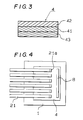
- FIG. 3 A typical layer structure of the insulating adhesive tape used according to the present Invention is shown in Fig. 3. That is, the insulating adhesive tape 4 used according to the present invention is formed, with an adhesive layer 42 of a thermoplastic polyimide being coated on one surface of the insulating base supporting film 41, and an adhesive layer 43 of a thermoplastic polyimide being coated onto the other surface of the insulating film 41, the adhesive layer 43 being a thermoplastic polyimide the same as or different from that of the first surface of the insulating film 41.
- the insulating adhesive tape 4 was tested using the device shown in Figs. 4, 5, and 6. As shown in these figures, the insulating adhesive tape 4 is adhered onto the IC chip 1 on which some leads 21 of lead frame 2 and a single test bar 8 for wire bonding are bonded.
- numeral 21a represents a silver plated portion of the lead 21.
- a gold wire 5 connects the silver plated portion 21a of the lead 21 to the test bar 8.
- a polymer with an imide bond may be used as a material for the insulating base supporting film 41.
- Such a material may be exemplified as follows: a polyimide film including Regulus (a trademark of Mitsui Toatsu Chemicals, Inc.) , Kapton H, V, E, K and ZT (respectively, a trademark of Du Pont Co.), Upilex M, S, SGA, SGAPA respectively, a trademark of Ube industries, Ltd.), Apical AH, NPI (respectively, a trademark of Kanegafuchi Chemical Industry Co., Ltd.), or an aramid film such as Aramica (a trademark of Asahi Chemical Industry Co., Ltd.).
- Regulus a trademark of Mitsui Toatsu Chemicals, Inc.
- Kapton H, V, E, K and ZT (respectively, a trademark of Du Pont Co.)
- Upilex M S, SGA, SGAPA respectively, a trademark of Ube industries, Ltd.
- Apical AH, NPI respectively, a trademark of Kanegafuchi Chemical Industry Co., Ltd.
- the thickness of the base film is not particularly limited. However, it is preferable that the thickness ranges from 1 to 500 ⁇ m, more preferably from 5 to 100 ⁇ m.
- thermoplastic polyimide layer Before a thermoplastic polyimide layer is formed on the base film, it is preferable to subject the surface of the substrate to a plasma treatment or ozone treatment. It is well-known to make rough physically the surface of a substrate by these treatments or to form chemically a functional group such as carboxyl radical on the same.
- thermoplastic polyimide layer of the present invention is remarkable beyond expectations.
- the adhesive strength to the substrate can be improved and stabilized largely.
- thermoplastic polyimide layer is formed on the treated surface of the base film.
- the thermoplastic polyimide forming the layer has a glass transition temperature ranging from 180°C to 280°C, and has a modulus of elasticity ranging 10 10 to 10 11 dyne/cm 2 at 25 °C, and a modulus ranging 10 2 to 10 9 dyne/cm 2 at a wire bonding temperature ranging from 250°C to 300°C.
- thermoplastic polyimide of PI-X, PI-Xh, PI-Y, PI-Yh, or PI-Z may be listed as a preferable thermoplastic polymer having the above mentioned properties.
- the glass transition temperature is less than 180°C or the modulus is less than 10 2 dyne/cm 2 at a wire bonding temperature, such a problem will occur that the inner lead is moved during wire bonding process or energy cannot properly be transferred to the inner lead in ultrasonic heating.
- the glass transition temperature is more than 280 °C or the modulus is more than 10 9 dyne/cm 2 at the wire bonding temperature, it will take much time to perform thermo-melting-bonding for the lead frame and IC chip, whereby it is difficult to execute a short time bonding.
- the amount of the solvent contained within the thermoplastic polyimide layer formed over the base film is not more than 1% and that the imide reaction of the thermoplastic polyimide has been substantially completed. This can prevent the solvent volatilization or the volatilization of moisture produced due to an imidization chemical reaction during the short time thermo-melting-bonding at high temperature (generally, over 270 °C) from contaminating the surface of the lead frame or IC chip, or producing void in the adhesive layer.
- a silane coupling agent is mixed and reacted at the rime when the thermoplastic polyimide coated over the base film is synthesized, or is mixed after the synthesizing process.
- the silane coupling agent such as followings may be recommended: that is, epoxy silane, thiol silane, amino silane (KBM-403, KBM-803, KBM-602, KBM-573, manufactured by Shin-Etsu Chemical Co., Ltd.), particularly, KBM-403 and KBM-803 is preferable.
- the amount of silane coupling agent to be used desirably ranges from not less than 0.5% by weight of the thermoplastic polyimide to not more than 4% by weight thereof, preferably from more than 1% by weight thereof to less than 3% by weight thereof.
- the amount of the silane coupling agent of less than 0.5% or more than 4% is not preferable because the humidity resistant adhesive strength to a ceramic or glass is poor, or the volatilization of an excessive silane coupling agent during the thermo-melting-bonding process at high temperature may contaminate the lead frame.
- the necessary requirements are that the glass transition temperature of the thermoplastic polymer ranges from 180°C to 280°C and the modulus of elasticity ranges from 10 10 to 10 11 dyne/cm 2 at 25°C, and from 10 2 to 10 9 dyne/cm 2 at a wire bonding temperature.
- the ionic impurities of sodium, potassium, chlorine, sulphate ion in the thermoplastic polymer is trace or about 1 ⁇ g/g (by the hydrothermal extracting method, it was calculated based on the amount of ions extracted from a water at 120°C for 24 hours).
- the amount of the radioactive element such as uranium, thorium causing software error in a semiconductor memory may be) less than the detection limit of a radioactivation analyzer i.e. less than 0.6 ppb, the reliability of the semiconductor memory can be maintained at a very higher level for long period.
- the water absorbing ratio of the thermoplastic polymer is preferably less than 1.2% (after immersing in a pure water at 23°C for 24 hours). Since the value is 1/2 to 1/5 of that of polyether amide and polyether amide-imide generally used, the void formation can be largely decreased be caused by possible water vapor during an adhering process under high temperature.
- the thermoplastic polyimide layer can be formed by coating a polyimide acid varnish containing a polyamide acid (as a polyimide precursor), a polyimide varnish containing polyimide, or a polyimide varnish containing a polyimide acid and silane coupling agent which is mixed and reacted when polyamide acid is synthesized, or is mixed after the synthesis, and then drying the coated layer to imidize the polyamide acid.
- a polyimide acid varnish containing a polyamide acid as a polyimide precursor
- a polyimide varnish containing polyimide or a polyimide varnish containing a polyimide acid and silane coupling agent which is mixed and reacted when polyamide acid is synthesized, or is mixed after the synthesis
- the varnish before the varnish is coated on the base film, the varnish, if necessary, may be mixed with a filler such as silica which does not contain a radio-active element such as uranium and thorium, or an epoxy resin such as EOCN-1027 (a trademark of Nippon Kayaku Co.,Ltd).
- a filler such as silica which does not contain a radio-active element such as uranium and thorium, or an epoxy resin such as EOCN-1027 (a trademark of Nippon Kayaku Co.,Ltd).
- thermoplastic polyimide layers are particularly not limited to the thickness thereof. However it is desirable that the thickness ranges from more than 1 ⁇ m to less than 100 ⁇ m, preferably from more than 3 ⁇ m to less than 50 ⁇ m.
- a conventional roll carrying drier may be used when the thermoplastic polymer layer is formed on one surface of the base film.
- a floating drier may be recommended when a thermoplastic polyimide is formed on the both surfaces of the base film.
- thermoplastic polyimide layer When the amount of the solvent contained within the thermoplastic polyimide layer is not more than 15% by weight, it is preferable to dry using a drier having a far infrared heater arranged between support rollers spaced by 1 to 5 m from each other in order to improve the adhesive property between the thermoplastic polyimide layer and the semiconductor material.
- the drying conditions depends on the thickness of the thermoplastic polyimide, the concentration of a varnish and the drying method. For example, when the varnish has its concentration of 25% and its thickness of 25 ⁇ m after drying, the drying is generally performed for 2 to 30 minutes at 100 to 150°C, 150 to 200°C, 200 to 250°C , or 250 to 300°C Temperatures over a range of 300 to 400°C can reduce the drying time to 10 minutes or less.
- thermoplastic polymer layer In order to reduce the amount of gas produced during a melting and pressing time, it is desirable that by these drying treatment to decrease the remaining solvent existing in the thermoplastic polymer layer to less than 1%, preferably to less than 0.1%, more preferably to less than 0.05%.
- drying processes converts the polyamide acid substantially into a polyimide.
- the drying is preferably performed in a cleanness of less than 1000, preferably less than 100, if necessary, in a nitrogen atmosphere with the same cleanness.
- a sheet of a width of 300mm or more is usually used as the base film, and a thermoplastic polyimide layer is formed thereon. Then the sheet may be cut to form a with a width suitable for use.
- the polyamide acid varnish or polyimide varnish for example, is manufactured as follows:
- a polyamide acid varnish being a polyimide precursor is prepared by solving an aromatic diamine in a polar solvent such as an N-methyl pyrrolidone, adding an aromatic tetracarboxylic acid anhydride within a range of 90 to 110% by equivalent ratio, and reacting them.
- This equivalent ratio is selected preferably to be within a range of 95 to 105%, more preferably to 97 to 102%.
- Such amide acid polymer has a logarithmic viscosity ⁇ of 0.3 to 3 dl/g (measured with an N, N-dimethylacetamide solvent medium of a concentration of 0.5g/100ml at 35 °C ), preferably 0.5 to 1.5 dl/g.
- PI-X, PI-Y, and PI-Z can be synthesized by performing the processes disclosed in Japanese Patent Application Laid-open Nos. SHO-61-291670 (1986), HEI-5-59344 (1993), and SHO-62-68817 (1987, same as USP 4,847,349).
- a dicarboxylic acid anhydride expressed by the following formula (2) may be used to cap the amine on the terminal of the amide acid: (where Z is a divalent radical selected from the group of monocyclic aromatic radical, condensed polycyclic aromatic radical, and non-condensed polycyclic aromatic radicals in which aromatic radicals are directly connected or mutually connected via cross linkers.)
- said cross linkers mean linking groups such as CO-, -O-, -S-, -SO 2 -, -CH 2 -, -C(CH 3 ) 2 - and -C(CF 3 ) 2 -.
- the dicarboxylic acid anhydride may be added at the earlier stage of the amide acid polymer producing process or after this process.
- the varnish of an amide acid polymer with the capped terminal of amine may be coated on the base film without any change.
- the above mentioned PI-Xh and PI-Yh can be synthesized using the methods disclosed in Japanese Patent Application Laid-open Nos. HEI-4-111167 (1992) and HEI-5-59344 (1993).
- PI-X, PI-Xh, PI-Y, PI-Yh and PI-Z when the polyamide acid varnish or polyimide varnish is prepared, as long as the properties of the varnish after drying is within the range of glass transition temperatures and modulus of elasticity at high temperature specified according to the present invention, a part of the aromatic diamine, aromatic tetracarboxylic acid anhydride, and dicarboxylic acid anhydride being polyamide acid or polyamide component, can be substituted with another sort of aromatic diamine, aromatic tetracarboxylic acid anhydride, or dicarboxylic acid anhydride without any trouble.
- diamines which can be used in combination include, for example, m-phenylenediamine, o-phenylenediamine, p-phenylenediamine, m-aminobenzylamine, o-aminobenzylamine,
- diamines can be used singly or as a mixture.
- Exemplary dianhydrides include:
- aromatic tetracarboxylic dianhydrides can be used singly or as a mixture.
- Aromatic diamine which can be used for the reaction includes, for example,
- Exemplary aromatic dicarboxylic anhydrides of the formula (2) include phthalic anhydride, 2,3-benzophenonedicarboxylic anhydride,
- Solvent which can be used include, for example, N-methyl-2-pyrrolidone, N,N-dimethylacetamide, N,N-dimethylformamide,, 1,3-dimethyl-2-imidazolidinone, N,N-diethylacetamide, N,N-dimethylmethoxyacetamide, dimethyl sulfoxide, pyridine, picoline, dimethyl sulfone, hexamethylphosphoramide, tetramethyl urea, N-methylcaprolactam, butyrolactam, tetrahydrofuran, 1,3-dioxane, 1,4-dioxane, 1,2-dimethoxyethane, bis(2-methoxyethyl) ether,1,2-bis(2-methoxyethoxy)ethane, bis[2-(2-methoxyethoxy) ethyl]ether, o-cresol, m-cresol, p-cresol, cresylic acid,
- the insulating adhesive tape and electronic components such as lead frames and IC chips can be adhered with each other by a well-known thermo-melting press-bonding method.
- the adhesive temperature is selected within the range of from 250°C to 450°C , and particularly from 270°C to 400°C .
- the adhesive time is particularly not limited but it is desirable to shorten the adhesive time as much as possible, usually to a range of 0.1 to 10 seconds, preferably to a range of 0.1 to 5 seconds. It is desirable to set the adhesive pressure to 1 to 50kg/cm 2 preferably to 5 to 30 kg/cm 2 .
- an oxygen concentration in an ambient of the thermo-melting press-bonding is set to less than 4%, preferably to less than 1%, to thus prevent an formation of an oxide layer.
- thermoplastic polyimide has an excellent adhesive property to a semiconductor material and its glass transition temperature is not less than 180°C (which is higher than 175°C of usual molding temperature of resin encapsulating material), superior moldability is given during resin encapsulating process with no deformation nor flow at thermoplastic nor being made.
- the glass transition temperatures as high as 180 ⁇ 280°C provide very good thermo-melting press-bonding conditions for industrial production.
- the modulus of elasticity as low as 10 2 to 10 9 dyne/cm 2 at 250 to 300 °C does not allow slightest movement of inner lead during the wire bonding step where an inner lead is wired with an IC chip at 240 to 280 °C thereby excellent reliability for bonding can be assured.
- the good bond is secured between an inner lead and an IC chip during a reflow soldering process.
- the volume specific resistance is 10 10 to 10 18 ⁇ cm
- the surface resistance is 10 10 to 10 18
- the ionic impurities are very scarce.
- the viscosity of the resultant polyimide varnish was 60 poise (at 25°C , E-type viscometer) and its logarithmic viscosity ⁇ was 0.55 dl/g.
- the viscosity of the resultant polyimide varnish was 8 Nsm -2 (80 poise) (at 25°C , E-type viscometer) and its logarithmic viscosity ⁇ was 0.60 dl/g.
- Insulating adhesive tapes were manufactured by using the varnish obtained by the above synthesis examples and various base films and were subjected to various tests. The test results are shown in the following Table.
- the varnish produced in the above synthesis example is coated over a base film.
- the sample is heated stepwise by 30°C temperature from 100°C to 250°C, while it is dried for 5 minutes in each step to imidate. Finally, a thermoplastic polyimide layer with a predetermined thickness is formed. Then, an adhesive insulating tape is prepared.
- thermoplastic polyimide used alone is processed into a film.
- the elastic modulus of the film is measured at 25 °C and 250°C using VIBRON (trademark) viscoelastometer.
- the insulating adhesive tape is cut into 10 mm square pieces.
- Each piece, as shown in Figs. 4 and 5, is placed on a Si chip 1 coated with polyimide, and the leads 21 of a comb-type lead frame of 42NiFe alloy is arranged on the piece.
- the structure is subjected to a thermo-press-bonding at 270°C for 5 seconds at a pressure of 30kg/cm 2 .
- the leads 21 are sheared out of the frame to form plural test samples M and S, as shown in Figs. 4 and 5.
- the lead frame used for testing are a comb-type lead frame with 16 leads.
- the width of the lead is 0.3mm and the gap between the leads is 0.3mm.
- the width of the lead is 0.15 mm and the gap between the leads is 0.15 mm.
- Each lead has a thickness of 0.15 mm and a silver plated portion at the area of 0.5 mm from the end.
- Samples M were subjected to aging test for a 90-degree peeling strength.
- the test samples S were subjected to an aging test for an insulation. In order to perform an aging test for the 90-degree peeling strength, some test samples M were measured for the initial 90-degree peeling strength. Other test samples M were subjected to the 90-degree peeling strength test after they had been left for 1000 hours in a pressure-cooker whose atmosphere has a temperature of 121°C and a relative humidity of 90%.
- a test bar 8 was adhered to the test sample S, as shown in Figs. 4 and 6, and the resultant structure was subjected to a wire bonding test.
- a bonding was carried out using a gold wire while an ultrasonic vibration is being applied under the condition of the stage temperature of 260°C and a bonding load of 100g. Thereafter, the positional deviation movement of lead 21 resulting from the bonding step was observed and bonding strength was measured.
- the insulating adhesive tape used according to the present invention can be adhered in very short time to the lead frame of resin encapsulated-type semiconductor devices, IC chips and heat spreaders.
- the excellent adhesive property and heat resistance can completely prevent the reduction of peeling strength and lead movement during the wire bonding process.
- the insulating adhesive tape used according to the present invention does not substantially exhibit adhesive strength decreasing and surface resistance decreasing after the 1000 hour durability test in a pressure-cooker being under the severe condition that the temperature is 121°C and the relative humidity is 90%.
- the adhesive performance can be largely improved to semiconductor material such as lead frame, IC chip, heat spreader, thus securing higher reliability to a long period service.
- the insulating adhesive tape also can make it possible to carry out bonding in a very short time operation, which is extremely important for the industrial field.
Landscapes
- Chemical & Material Sciences (AREA)
- Chemical Kinetics & Catalysis (AREA)
- Physics & Mathematics (AREA)
- Spectroscopy & Molecular Physics (AREA)
- Organic Chemistry (AREA)
- Polymers & Plastics (AREA)
- Medicinal Chemistry (AREA)
- Health & Medical Sciences (AREA)
- Adhesive Tapes (AREA)
- Adhesives Or Adhesive Processes (AREA)
- Laminated Bodies (AREA)
- Lead Frames For Integrated Circuits (AREA)
- Die Bonding (AREA)
Claims (12)
- Verwendung eines isolierenden Klebebands zum Aufkleben eines Halbleiters auf einen Metall-Leiter, wobei das Band eines Basisträgerfilm und eine auf zumindest einer Oberfläche davon ausgebildete Kleberschicht umfaßt, wobei die Kleberschicht im wesentlichen aus einem thermoplastischen Polyimid und gegebenenfalls einem Füllstoff besteht, wobei das Polyimid aus Struktureinheiten der folgenden Formel (1)oder Struktureinheiten der folgenden Formel (3)
 besteht, worin: m:n = (1-90) : (99-10) ist; oder n=0 ist, worin das thermoplastische Polyimid eine Glastemperatur im Bereich von 180°c bis 280°C und einen Elastizitätsmodul bei 25°C im Bereich von 1010 dyn/cm2 bis 1011 dyn/cm2 aufweist, wobei der Modul bei einer Temperatur zwischen 150°C und 300°C einen Wert im Bereich von 102 dyn/cm2 bis 109 dyn/cm2 aufweist.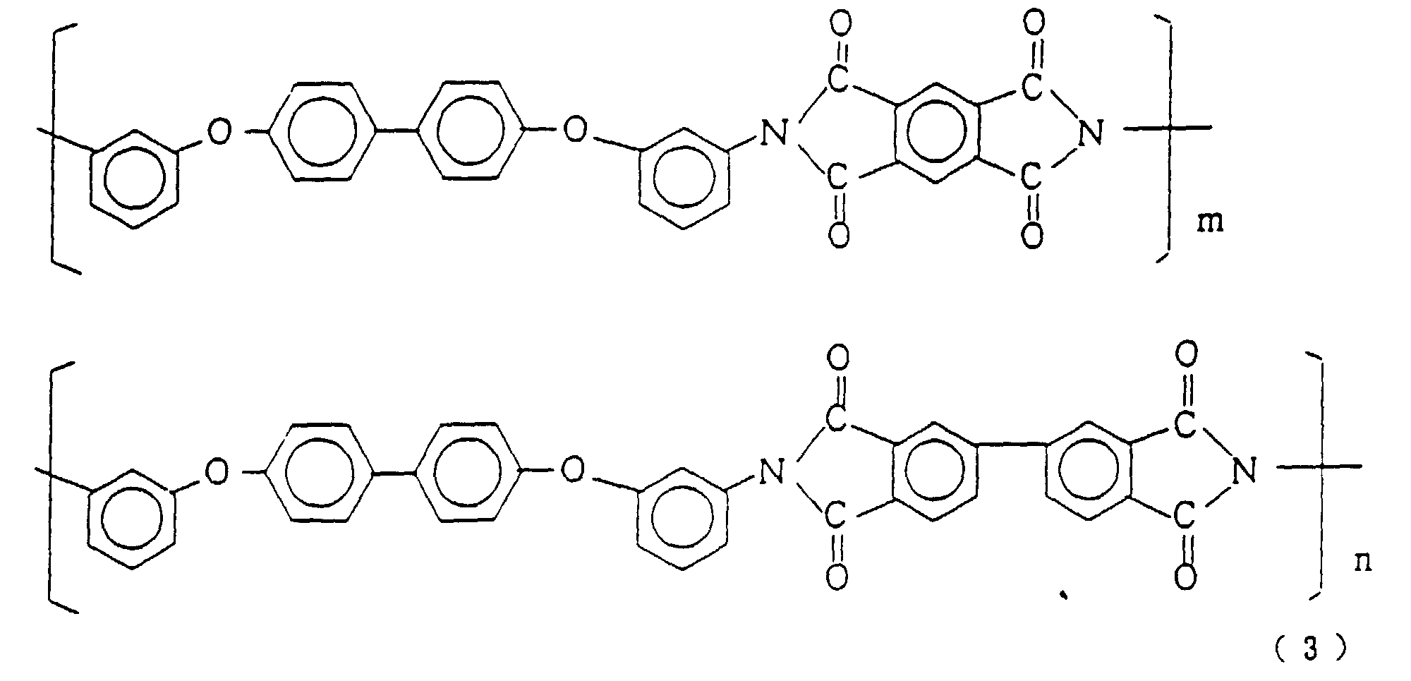
- Verwendung nach Anspruch 1, worin das thermoplastische Polyimid eine Glastemperatur im Bereich von 180°C bis 240°C und einen Elastizitätsmodul im Bereich von 102 dyn/cm2 bis 109 dyn/cm2 bei 250°C aufweist.
- Verwendung nach Anspruch 1, worin das thermoplastische Polyimid eine Glastemperatur im Bereich von 200°C bis 260°C und einen Elastizitätsmodul bei 270°C im Bereich von 102 dyn/cm2 bis 109 dyn/cm2 aufweist.
- Verwendung nach Anspruch 1, worin das thermoplastische Polyimid eine Glastemperatur im Bereich von 250°C bis 280°C und einen Elastizitätsmodul bei einer Temperatur zwischen 270°C und 300°C im Bereich von 102 dyn/cm2 bis 109 dyn/cm2 aufweist.
- Verwendung nach einem der vorangegangenen Ansprüche, worin die Oberfläche des Basisträgerfilms einer Plasmabehandlung oder Ozonbehandlung unterzogen wurde.
- Verwendung nach einem der vorangegangenen Ansprüche, worin das thermoplastische Polyimid ein mit Silan-Haftverbesserer modifiziertes thermoplastisches Polyimid umfaßt.
- Verwendung nach einem der vorangegangenen Ansprüche mit der Maßgabe, daß n≠0 ist, und worin das thermoplastische Polyimid mit einem Dicarbonsäureanhydrid der folgenden Formel (2) verkappt ist:worin Z ein zweiwertiger Rest, ausgewählt aus der aus monozyklischen aromatischen Resten, kondensierten polyzyklischen aromatischen Resten und nichtkondensierten polyzyklischen aromatischen Resten, bei denen die aromatischen Reste direkt oder über Vernetzer miteinander verbunden sind, bestehenden Gruppe, ist.

- Leiterplatte, die innere Leiter aufweist, die mit einem isolierenden Klebeband nach einem der vorangegangenen Ansprüche fixiert sind.
- Leiterplatte nach Anspruch 8, worin das isolierende Klebeband, mit dem die inneren Leiter fixiert sind, an beiden Oberflächen Kleberschichten aufweist, wobei jede der Kleberschichten im wesentlichen aus einem thermoplastischen Polyimid besteht, eine Oberfläche der Kleberschicht die inneren Leiter fixiert und die andere Oberfläche der Kleberschicht auf einen IC-Chip oder einen Wärmeverteiler aufkleibbar ist.
- Halbleitervorrichtung, die eine Leiterplatte nach Anspruch 8 oder 9 umfaßt; wobei zumindest der Abschnitt der inneren Leiter, der mit dem isolierenden Klebeband fixiert ist, mit einem Harz verkapselt ist.
- Halbleitervorrichtung nach Anspruch 10, worin die Halbleitervorrichtung vom Leiter-auf-Chip-Typ ist.
- Halbleitervorrichtung nach Anspruch 10, worin die Halbleitervorrichtung vom Typ einer Leiterplatte mit Wärmeverleiler ist.
Applications Claiming Priority (6)
| Application Number | Priority Date | Filing Date | Title |
|---|---|---|---|
| JP325434/92 | 1992-12-04 | ||
| JP325435/92 | 1992-12-04 | ||
| JP32543492 | 1992-12-04 | ||
| JP32543592 | 1992-12-04 | ||
| JP5000259A JP2866779B2 (ja) | 1993-01-05 | 1993-01-05 | 耐熱性接着シート |
| JP259/93 | 1993-01-05 |
Publications (3)
| Publication Number | Publication Date |
|---|---|
| EP0605112A2 EP0605112A2 (de) | 1994-07-06 |
| EP0605112A3 EP0605112A3 (en) | 1995-08-16 |
| EP0605112B1 true EP0605112B1 (de) | 1999-03-17 |
Family
ID=27274376
Family Applications (1)
| Application Number | Title | Priority Date | Filing Date |
|---|---|---|---|
| EP19930309704 Expired - Lifetime EP0605112B1 (de) | 1992-12-04 | 1993-12-03 | Verwendung eines isolierenden Klebebandes, Leiterplatte und Halbleiteranordnung mit diesem Band |
Country Status (5)
| Country | Link |
|---|---|
| US (1) | US5406124A (de) |
| EP (1) | EP0605112B1 (de) |
| KR (2) | KR0134165B1 (de) |
| DE (1) | DE69323984T2 (de) |
| SG (1) | SG47438A1 (de) |
Families Citing this family (182)
| Publication number | Priority date | Publication date | Assignee | Title |
|---|---|---|---|---|
| US5849607A (en) * | 1993-11-27 | 1998-12-15 | Samsung Electronics Co., Ltd. | Process for attaching a lead frame to a semiconductor chip |
| US5434105A (en) * | 1994-03-04 | 1995-07-18 | National Semiconductor Corporation | Process for attaching a lead frame to a heat sink using a glob-top encapsulation |
| US5665473A (en) * | 1994-09-16 | 1997-09-09 | Tokuyama Corporation | Package for mounting a semiconductor device |
| KR100333452B1 (ko) * | 1994-12-26 | 2002-04-18 | 이사오 우치가사키 | 필름 형상의 유기 다이본딩재 및 이를 이용한 반도체 장치 |
| JPH08222681A (ja) * | 1995-02-14 | 1996-08-30 | Toshiba Corp | 樹脂封止型半導体装置 |
| US6717242B2 (en) | 1995-07-06 | 2004-04-06 | Hitachi Chemical Company, Ltd. | Semiconductor device and process for fabrication thereof |
| TW310481B (de) * | 1995-07-06 | 1997-07-11 | Hitachi Chemical Co Ltd | |
| US6099678A (en) * | 1995-12-26 | 2000-08-08 | Hitachi Chemical Company Ltd. | Laminating method of film-shaped organic die-bonding material, die-bonding method, laminating machine and die-bonding apparatus, semiconductor device, and fabrication process of semiconductor device |
| KR0179803B1 (ko) * | 1995-12-29 | 1999-03-20 | 문정환 | 리드노출형 반도체 패키지 |
| US5872398A (en) * | 1996-01-11 | 1999-02-16 | Micron Technology, Inc. | Reduced stress LOC assembly including cantilevered leads |
| TW326566B (en) * | 1996-04-19 | 1998-02-11 | Hitachi Chemical Co Ltd | Composite film and lead frame with composite film attached |
| JP3195236B2 (ja) * | 1996-05-30 | 2001-08-06 | 株式会社日立製作所 | 接着フィルムを有する配線テープ,半導体装置及び製造方法 |
| TW422874B (en) * | 1996-10-08 | 2001-02-21 | Hitachi Chemical Co Ltd | Semiconductor device, semiconductor chip mounting substrate, methods of manufacturing the device and substrate, adhesive, and adhesive double coated film |
| JP3982895B2 (ja) * | 1997-04-09 | 2007-09-26 | 三井化学株式会社 | 金属ベース半導体回路基板 |
| JPH10330724A (ja) | 1997-05-30 | 1998-12-15 | Hitachi Chem Co Ltd | 耐熱接着剤、耐熱接着剤層付き半導体チップ、耐熱接着剤層付きリードフレーム、耐熱接着剤層付きフィルム及び半導体装置 |
| US6159764A (en) * | 1997-07-02 | 2000-12-12 | Micron Technology, Inc. | Varied-thickness heat sink for integrated circuit (IC) packages and method of fabricating IC packages |
| WO1999041783A1 (de) * | 1998-02-12 | 1999-08-19 | Siemens Aktiengesellschaft | Halbleiterbaugruppe |
| US7270867B1 (en) | 1998-06-10 | 2007-09-18 | Asat Ltd. | Leadless plastic chip carrier |
| US6229200B1 (en) | 1998-06-10 | 2001-05-08 | Asat Limited | Saw-singulated leadless plastic chip carrier |
| US8330270B1 (en) | 1998-06-10 | 2012-12-11 | Utac Hong Kong Limited | Integrated circuit package having a plurality of spaced apart pad portions |
| JP3853979B2 (ja) * | 1998-06-16 | 2006-12-06 | 日東電工株式会社 | 半導体装置の製法 |
| US6143981A (en) | 1998-06-24 | 2000-11-07 | Amkor Technology, Inc. | Plastic integrated circuit package and method and leadframe for making the package |
| US7030474B1 (en) | 1998-06-24 | 2006-04-18 | Amkor Technology, Inc. | Plastic integrated circuit package and method and leadframe for making the package |
| US7112474B1 (en) | 1998-06-24 | 2006-09-26 | Amkor Technology, Inc. | Method of making an integrated circuit package |
| US7005326B1 (en) | 1998-06-24 | 2006-02-28 | Amkor Technology, Inc. | Method of making an integrated circuit package |
| US6893900B1 (en) | 1998-06-24 | 2005-05-17 | Amkor Technology, Inc. | Method of making an integrated circuit package |
| US7071541B1 (en) | 1998-06-24 | 2006-07-04 | Amkor Technology, Inc. | Plastic integrated circuit package and method and leadframe for making the package |
| US7332375B1 (en) | 1998-06-24 | 2008-02-19 | Amkor Technology, Inc. | Method of making an integrated circuit package |
| KR100317648B1 (ko) * | 1998-08-26 | 2002-02-19 | 윤종용 | 절연접착테이프에의하여다이접착되는반도체소자및다이접착방법그리고그장치 |
| US6326687B1 (en) * | 1998-09-01 | 2001-12-04 | Micron Technology, Inc. | IC package with dual heat spreaders |
| US6281568B1 (en) | 1998-10-21 | 2001-08-28 | Amkor Technology, Inc. | Plastic integrated circuit device package and leadframe having partially undercut leads and die pad |
| US6329713B1 (en) * | 1998-10-21 | 2001-12-11 | International Business Machines Corporation | Integrated circuit chip carrier assembly comprising a stiffener attached to a dielectric substrate |
| US6448633B1 (en) * | 1998-11-20 | 2002-09-10 | Amkor Technology, Inc. | Semiconductor package and method of making using leadframe having lead locks to secure leads to encapsulant |
| US6303981B1 (en) * | 1999-09-01 | 2001-10-16 | Micron Technology, Inc. | Semiconductor package having stacked dice and leadframes and method of fabrication |
| KR20010037247A (ko) | 1999-10-15 | 2001-05-07 | 마이클 디. 오브라이언 | 반도체패키지 |
| KR100379089B1 (ko) | 1999-10-15 | 2003-04-08 | 앰코 테크놀로지 코리아 주식회사 | 리드프레임 및 이를 이용한 반도체패키지 |
| KR100526844B1 (ko) * | 1999-10-15 | 2005-11-08 | 앰코 테크놀로지 코리아 주식회사 | 반도체패키지 및 그 제조방법 |
| KR100403142B1 (ko) * | 1999-10-15 | 2003-10-30 | 앰코 테크놀로지 코리아 주식회사 | 반도체패키지 |
| US6580159B1 (en) | 1999-11-05 | 2003-06-17 | Amkor Technology, Inc. | Integrated circuit device packages and substrates for making the packages |
| US20070176287A1 (en) * | 1999-11-05 | 2007-08-02 | Crowley Sean T | Thin integrated circuit device packages for improved radio frequency performance |
| US6847103B1 (en) | 1999-11-09 | 2005-01-25 | Amkor Technology, Inc. | Semiconductor package with exposed die pad and body-locking leadframe |
| US6476478B1 (en) | 1999-11-12 | 2002-11-05 | Amkor Technology, Inc. | Cavity semiconductor package with exposed leads and die pad |
| US6639308B1 (en) * | 1999-12-16 | 2003-10-28 | Amkor Technology, Inc. | Near chip size semiconductor package |
| KR100421774B1 (ko) * | 1999-12-16 | 2004-03-10 | 앰코 테크놀로지 코리아 주식회사 | 반도체패키지 및 그 제조 방법 |
| DE10008121B4 (de) * | 2000-02-22 | 2006-03-09 | Saehan Micronics Inc. | Verfahren zur Herstellung von Polyamidsäure und Polyimid und Haft- oder Klebemittel, das aus der oder dem so hergestellten Polyamidsäure oder Polyimid besteht |
| KR100559664B1 (ko) | 2000-03-25 | 2006-03-10 | 앰코 테크놀로지 코리아 주식회사 | 반도체패키지 |
| KR100583494B1 (ko) * | 2000-03-25 | 2006-05-24 | 앰코 테크놀로지 코리아 주식회사 | 반도체패키지 |
| JP4349600B2 (ja) * | 2000-04-20 | 2009-10-21 | 大日本印刷株式会社 | 積層体、絶縁フィルム、電子回路及び積層体の製造方法 |
| US7042068B2 (en) | 2000-04-27 | 2006-05-09 | Amkor Technology, Inc. | Leadframe and semiconductor package made using the leadframe |
| JP4665298B2 (ja) * | 2000-08-25 | 2011-04-06 | 東レ株式会社 | 半導体装置用接着剤付きテープおよびそれを用いた銅張り積層板、半導体接続用基板ならびに半導体装置 |
| US6476182B1 (en) | 2000-12-21 | 2002-11-05 | E. I. Du Pont De Nemours And Company | Melt-processible, thermoplastic random copolyimides having recoverable crystallinity and associated processes |
| US6476177B2 (en) | 2000-12-21 | 2002-11-05 | E. I. Du Pont De Nemours And Company | Melt-processible, thermoplastic random copolyimides having recoverable crystallinity and associated processes |
| US6469126B1 (en) | 2000-12-21 | 2002-10-22 | E. I. Du Pont De Nmeours And Company | Melt-processible, thermoplastic random copolyimides having recoverable crystallinity and associated processes |
| US6444783B1 (en) | 2000-12-21 | 2002-09-03 | E. I. Du Pont De Nemours And Company | Melt-processible semicrystalline block copolyimides |
| KR20020058209A (ko) * | 2000-12-29 | 2002-07-12 | 마이클 디. 오브라이언 | 반도체패키지 |
| KR100394030B1 (ko) * | 2001-01-15 | 2003-08-06 | 앰코 테크놀로지 코리아 주식회사 | 적층형 반도체 패키지 |
| KR100731007B1 (ko) * | 2001-01-15 | 2007-06-22 | 앰코 테크놀로지 코리아 주식회사 | 적층형 반도체 패키지 |
| US6605865B2 (en) | 2001-03-19 | 2003-08-12 | Amkor Technology, Inc. | Semiconductor package with optimized leadframe bonding strength |
| US6967395B1 (en) | 2001-03-20 | 2005-11-22 | Amkor Technology, Inc. | Mounting for a package containing a chip |
| US6545345B1 (en) | 2001-03-20 | 2003-04-08 | Amkor Technology, Inc. | Mounting for a package containing a chip |
| KR100369393B1 (ko) | 2001-03-27 | 2003-02-05 | 앰코 테크놀로지 코리아 주식회사 | 리드프레임 및 이를 이용한 반도체패키지와 그 제조 방법 |
| KR100393448B1 (ko) * | 2001-03-27 | 2003-08-02 | 앰코 테크놀로지 코리아 주식회사 | 반도체 패키지 및 그 제조 방법 |
| US7045883B1 (en) | 2001-04-04 | 2006-05-16 | Amkor Technology, Inc. | Thermally enhanced chip scale lead on chip semiconductor package and method of making same |
| US7064009B1 (en) | 2001-04-04 | 2006-06-20 | Amkor Technology, Inc. | Thermally enhanced chip scale lead on chip semiconductor package and method of making same |
| US6756658B1 (en) | 2001-04-06 | 2004-06-29 | Amkor Technology, Inc. | Making two lead surface mounting high power microleadframe semiconductor packages |
| CN1285647C (zh) * | 2001-06-15 | 2006-11-22 | 钟渊化学工业株式会社 | 半导电性聚酰亚胺膜及其制造方法 |
| JP2003092379A (ja) * | 2001-09-18 | 2003-03-28 | Hitachi Ltd | 半導体装置 |
| US7485952B1 (en) | 2001-09-19 | 2009-02-03 | Amkor Technology, Inc. | Drop resistant bumpers for fully molded memory cards |
| US6900527B1 (en) | 2001-09-19 | 2005-05-31 | Amkor Technology, Inc. | Lead-frame method and assembly for interconnecting circuits within a circuit module |
| US6611047B2 (en) | 2001-10-12 | 2003-08-26 | Amkor Technology, Inc. | Semiconductor package with singulation crease |
| US6630726B1 (en) | 2001-11-07 | 2003-10-07 | Amkor Technology, Inc. | Power semiconductor package with strap |
| US6638835B2 (en) * | 2001-12-11 | 2003-10-28 | Intel Corporation | Method for bonding and debonding films using a high-temperature polymer |
| US6798046B1 (en) | 2002-01-22 | 2004-09-28 | Amkor Technology, Inc. | Semiconductor package including ring structure connected to leads with vertically downset inner ends |
| US6885086B1 (en) | 2002-03-05 | 2005-04-26 | Amkor Technology, Inc. | Reduced copper lead frame for saw-singulated chip package |
| US6608366B1 (en) | 2002-04-15 | 2003-08-19 | Harry J. Fogelson | Lead frame with plated end leads |
| SG109496A1 (en) * | 2002-04-22 | 2005-03-30 | Saehan Micronics Inc | Composite film and lead frame with composite film attached |
| US6627977B1 (en) | 2002-05-09 | 2003-09-30 | Amkor Technology, Inc. | Semiconductor package including isolated ring structure |
| US6841414B1 (en) | 2002-06-19 | 2005-01-11 | Amkor Technology, Inc. | Saw and etch singulation method for a chip package |
| US6867071B1 (en) | 2002-07-12 | 2005-03-15 | Amkor Technology, Inc. | Leadframe including corner leads and semiconductor package using same |
| EP1576623B1 (de) * | 2002-08-13 | 2007-01-10 | Dinesh M. Anam | Reibungs- und release- beschichteter polyimidfilm für elektrische isolierung sowie ein prozess zur herstellung |
| US7732914B1 (en) | 2002-09-03 | 2010-06-08 | Mclellan Neil | Cavity-type integrated circuit package |
| US6818973B1 (en) | 2002-09-09 | 2004-11-16 | Amkor Technology, Inc. | Exposed lead QFP package fabricated through the use of a partial saw process |
| US6919620B1 (en) | 2002-09-17 | 2005-07-19 | Amkor Technology, Inc. | Compact flash memory card with clamshell leadframe |
| US7190062B1 (en) | 2004-06-15 | 2007-03-13 | Amkor Technology, Inc. | Embedded leadframe semiconductor package |
| US7361533B1 (en) | 2002-11-08 | 2008-04-22 | Amkor Technology, Inc. | Stacked embedded leadframe |
| US7723210B2 (en) | 2002-11-08 | 2010-05-25 | Amkor Technology, Inc. | Direct-write wafer level chip scale package |
| US6905914B1 (en) | 2002-11-08 | 2005-06-14 | Amkor Technology, Inc. | Wafer level package and fabrication method |
| US7026436B2 (en) * | 2002-11-26 | 2006-04-11 | E.I. Du Pont De Nemours And Company | Low temperature polyimide adhesive compositions and methods relating thereto |
| US6798047B1 (en) | 2002-12-26 | 2004-09-28 | Amkor Technology, Inc. | Pre-molded leadframe |
| US6847099B1 (en) | 2003-02-05 | 2005-01-25 | Amkor Technology Inc. | Offset etched corner leads for semiconductor package |
| US6750545B1 (en) | 2003-02-28 | 2004-06-15 | Amkor Technology, Inc. | Semiconductor package capable of die stacking |
| US6927483B1 (en) | 2003-03-07 | 2005-08-09 | Amkor Technology, Inc. | Semiconductor package exhibiting efficient lead placement |
| US6794740B1 (en) | 2003-03-13 | 2004-09-21 | Amkor Technology, Inc. | Leadframe package for semiconductor devices |
| US7001799B1 (en) | 2003-03-13 | 2006-02-21 | Amkor Technology, Inc. | Method of making a leadframe for semiconductor devices |
| US6879034B1 (en) | 2003-05-01 | 2005-04-12 | Amkor Technology, Inc. | Semiconductor package including low temperature co-fired ceramic substrate |
| US7095103B1 (en) | 2003-05-01 | 2006-08-22 | Amkor Technology, Inc. | Leadframe based memory card |
| JP4359242B2 (ja) * | 2003-05-14 | 2009-11-04 | 三井化学株式会社 | 接着性樹脂組成物及びフィルム状接着剤並びにそれを用いた半導体装置 |
| US7008825B1 (en) | 2003-05-27 | 2006-03-07 | Amkor Technology, Inc. | Leadframe strip having enhanced testability |
| CN101447413B (zh) * | 2003-06-06 | 2013-03-27 | 日立化成株式会社 | 粘合片、与切割胶带一体化粘合片以及半导体的制造方法 |
| US6897550B1 (en) | 2003-06-11 | 2005-05-24 | Amkor Technology, Inc. | Fully-molded leadframe stand-off feature |
| US7033517B1 (en) | 2003-09-15 | 2006-04-25 | Asat Ltd. | Method of fabricating a leadless plastic chip carrier |
| US7245007B1 (en) | 2003-09-18 | 2007-07-17 | Amkor Technology, Inc. | Exposed lead interposer leadframe package |
| US6921967B2 (en) * | 2003-09-24 | 2005-07-26 | Amkor Technology, Inc. | Reinforced die pad support structure |
| US7138707B1 (en) | 2003-10-21 | 2006-11-21 | Amkor Technology, Inc. | Semiconductor package including leads and conductive posts for providing increased functionality |
| US7144517B1 (en) | 2003-11-07 | 2006-12-05 | Amkor Technology, Inc. | Manufacturing method for leadframe and for semiconductor package using the leadframe |
| US20050183769A1 (en) * | 2003-11-10 | 2005-08-25 | Hiroki Nakagawa | Method of producing substrate for dye-sensitized solar cell and dye-sensitized solar cell |
| US7211879B1 (en) | 2003-11-12 | 2007-05-01 | Amkor Technology, Inc. | Semiconductor package with chamfered corners and method of manufacturing the same |
| US7057268B1 (en) | 2004-01-27 | 2006-06-06 | Amkor Technology, Inc. | Cavity case with clip/plug for use on multi-media card |
| US7091594B1 (en) | 2004-01-28 | 2006-08-15 | Amkor Technology, Inc. | Leadframe type semiconductor package having reduced inductance and its manufacturing method |
| US20080003722A1 (en) * | 2004-04-15 | 2008-01-03 | Chun David D | Transfer mold solution for molded multi-media card |
| CN100441619C (zh) * | 2004-04-30 | 2008-12-10 | 株式会社吴羽 | 封装用树脂组合物以及树脂封装的半导体装置 |
| US7411289B1 (en) | 2004-06-14 | 2008-08-12 | Asat Ltd. | Integrated circuit package with partially exposed contact pads and process for fabricating the same |
| US7091581B1 (en) | 2004-06-14 | 2006-08-15 | Asat Limited | Integrated circuit package and process for fabricating the same |
| US7202554B1 (en) | 2004-08-19 | 2007-04-10 | Amkor Technology, Inc. | Semiconductor package and its manufacturing method |
| US20070292701A1 (en) * | 2004-09-24 | 2007-12-20 | Takashi Kikuchi | Novel Polyimide Film Improved in Adhesion |
| US7595225B1 (en) | 2004-10-05 | 2009-09-29 | Chun Ho Fan | Leadless plastic chip carrier with contact standoff |
| US7217991B1 (en) | 2004-10-22 | 2007-05-15 | Amkor Technology, Inc. | Fan-in leadframe semiconductor package |
| US7358119B2 (en) * | 2005-01-12 | 2008-04-15 | Asat Ltd. | Thin array plastic package without die attach pad and process for fabricating the same |
| CN101098909B (zh) * | 2005-01-18 | 2010-07-28 | 株式会社钟化 | 粘合性经改良的新的聚酰亚胺薄膜 |
| CN101667493B (zh) * | 2005-03-30 | 2012-09-26 | 大日本印刷株式会社 | 氧化物半导体电极、色素增感型太阳能电池及它们的制造方法 |
| US20060219294A1 (en) * | 2005-03-30 | 2006-10-05 | Dai Nippon Printing Co., Ltd. | Oxide semiconductor electrode, dye-sensitized solar cell, and, method of producing the same |
| US7348663B1 (en) | 2005-07-15 | 2008-03-25 | Asat Ltd. | Integrated circuit package and method for fabricating same |
| DE102005034873B4 (de) * | 2005-07-26 | 2013-03-07 | Siemens Aktiengesellschaft | Anordnung eines elektrischen Bauelements und eines auf dem Bauelement auflaminierten Folienverbunds und Verfahren zur Herstellung der Anordnung |
| US7410830B1 (en) | 2005-09-26 | 2008-08-12 | Asat Ltd | Leadless plastic chip carrier and method of fabricating same |
| US7507603B1 (en) | 2005-12-02 | 2009-03-24 | Amkor Technology, Inc. | Etch singulated semiconductor package |
| US7572681B1 (en) | 2005-12-08 | 2009-08-11 | Amkor Technology, Inc. | Embedded electronic component package |
| US7902660B1 (en) | 2006-05-24 | 2011-03-08 | Amkor Technology, Inc. | Substrate for semiconductor device and manufacturing method thereof |
| US7968998B1 (en) | 2006-06-21 | 2011-06-28 | Amkor Technology, Inc. | Side leaded, bottom exposed pad and bottom exposed lead fusion quad flat semiconductor package |
| US7687893B2 (en) | 2006-12-27 | 2010-03-30 | Amkor Technology, Inc. | Semiconductor package having leadframe with exposed anchor pads |
| US7829990B1 (en) | 2007-01-18 | 2010-11-09 | Amkor Technology, Inc. | Stackable semiconductor package including laminate interposer |
| US7982297B1 (en) | 2007-03-06 | 2011-07-19 | Amkor Technology, Inc. | Stackable semiconductor package having partially exposed semiconductor die and method of fabricating the same |
| US7977774B2 (en) | 2007-07-10 | 2011-07-12 | Amkor Technology, Inc. | Fusion quad flat semiconductor package |
| US7687899B1 (en) | 2007-08-07 | 2010-03-30 | Amkor Technology, Inc. | Dual laminate package structure with embedded elements |
| US7777351B1 (en) | 2007-10-01 | 2010-08-17 | Amkor Technology, Inc. | Thin stacked interposer package |
| US8089159B1 (en) | 2007-10-03 | 2012-01-03 | Amkor Technology, Inc. | Semiconductor package with increased I/O density and method of making the same |
| US7847386B1 (en) | 2007-11-05 | 2010-12-07 | Amkor Technology, Inc. | Reduced size stacked semiconductor package and method of making the same |
| US7956453B1 (en) | 2008-01-16 | 2011-06-07 | Amkor Technology, Inc. | Semiconductor package with patterning layer and method of making same |
| US7723852B1 (en) | 2008-01-21 | 2010-05-25 | Amkor Technology, Inc. | Stacked semiconductor package and method of making same |
| US8067821B1 (en) | 2008-04-10 | 2011-11-29 | Amkor Technology, Inc. | Flat semiconductor package with half package molding |
| US7768135B1 (en) | 2008-04-17 | 2010-08-03 | Amkor Technology, Inc. | Semiconductor package with fast power-up cycle and method of making same |
| US7808084B1 (en) | 2008-05-06 | 2010-10-05 | Amkor Technology, Inc. | Semiconductor package with half-etched locking features |
| US8125064B1 (en) | 2008-07-28 | 2012-02-28 | Amkor Technology, Inc. | Increased I/O semiconductor package and method of making same |
| US8184453B1 (en) | 2008-07-31 | 2012-05-22 | Amkor Technology, Inc. | Increased capacity semiconductor package |
| US7847392B1 (en) | 2008-09-30 | 2010-12-07 | Amkor Technology, Inc. | Semiconductor device including leadframe with increased I/O |
| US7989933B1 (en) | 2008-10-06 | 2011-08-02 | Amkor Technology, Inc. | Increased I/O leadframe and semiconductor device including same |
| US8008758B1 (en) | 2008-10-27 | 2011-08-30 | Amkor Technology, Inc. | Semiconductor device with increased I/O leadframe |
| US8089145B1 (en) | 2008-11-17 | 2012-01-03 | Amkor Technology, Inc. | Semiconductor device including increased capacity leadframe |
| US8072050B1 (en) | 2008-11-18 | 2011-12-06 | Amkor Technology, Inc. | Semiconductor device with increased I/O leadframe including passive device |
| US7875963B1 (en) | 2008-11-21 | 2011-01-25 | Amkor Technology, Inc. | Semiconductor device including leadframe having power bars and increased I/O |
| US7982298B1 (en) | 2008-12-03 | 2011-07-19 | Amkor Technology, Inc. | Package in package semiconductor device |
| US8487420B1 (en) | 2008-12-08 | 2013-07-16 | Amkor Technology, Inc. | Package in package semiconductor device with film over wire |
| US8680656B1 (en) | 2009-01-05 | 2014-03-25 | Amkor Technology, Inc. | Leadframe structure for concentrated photovoltaic receiver package |
| US20170117214A1 (en) | 2009-01-05 | 2017-04-27 | Amkor Technology, Inc. | Semiconductor device with through-mold via |
| US8058715B1 (en) | 2009-01-09 | 2011-11-15 | Amkor Technology, Inc. | Package in package device for RF transceiver module |
| US8026589B1 (en) | 2009-02-23 | 2011-09-27 | Amkor Technology, Inc. | Reduced profile stackable semiconductor package |
| US7960818B1 (en) | 2009-03-04 | 2011-06-14 | Amkor Technology, Inc. | Conformal shield on punch QFN semiconductor package |
| US8575742B1 (en) | 2009-04-06 | 2013-11-05 | Amkor Technology, Inc. | Semiconductor device with increased I/O leadframe including power bars |
| CN102024708A (zh) * | 2009-09-14 | 2011-04-20 | 飞思卡尔半导体公司 | 引线框及其形成方法 |
| US8796561B1 (en) | 2009-10-05 | 2014-08-05 | Amkor Technology, Inc. | Fan out build up substrate stackable package and method |
| US8937381B1 (en) | 2009-12-03 | 2015-01-20 | Amkor Technology, Inc. | Thin stackable package and method |
| US9691734B1 (en) | 2009-12-07 | 2017-06-27 | Amkor Technology, Inc. | Method of forming a plurality of electronic component packages |
| US8324511B1 (en) | 2010-04-06 | 2012-12-04 | Amkor Technology, Inc. | Through via nub reveal method and structure |
| US8294276B1 (en) | 2010-05-27 | 2012-10-23 | Amkor Technology, Inc. | Semiconductor device and fabricating method thereof |
| US8440554B1 (en) | 2010-08-02 | 2013-05-14 | Amkor Technology, Inc. | Through via connected backside embedded circuit features structure and method |
| US8487445B1 (en) | 2010-10-05 | 2013-07-16 | Amkor Technology, Inc. | Semiconductor device having through electrodes protruding from dielectric layer |
| US8791501B1 (en) | 2010-12-03 | 2014-07-29 | Amkor Technology, Inc. | Integrated passive device structure and method |
| US8674485B1 (en) | 2010-12-08 | 2014-03-18 | Amkor Technology, Inc. | Semiconductor device including leadframe with downsets |
| US8390130B1 (en) | 2011-01-06 | 2013-03-05 | Amkor Technology, Inc. | Through via recessed reveal structure and method |
| US8648450B1 (en) | 2011-01-27 | 2014-02-11 | Amkor Technology, Inc. | Semiconductor device including leadframe with a combination of leads and lands |
| TWI557183B (zh) | 2015-12-16 | 2016-11-11 | 財團法人工業技術研究院 | 矽氧烷組成物、以及包含其之光電裝置 |
| US8552548B1 (en) | 2011-11-29 | 2013-10-08 | Amkor Technology, Inc. | Conductive pad on protruding through electrode semiconductor device |
| US9704725B1 (en) | 2012-03-06 | 2017-07-11 | Amkor Technology, Inc. | Semiconductor device with leadframe configured to facilitate reduced burr formation |
| US9048298B1 (en) | 2012-03-29 | 2015-06-02 | Amkor Technology, Inc. | Backside warpage control structure and fabrication method |
| US9129943B1 (en) | 2012-03-29 | 2015-09-08 | Amkor Technology, Inc. | Embedded component package and fabrication method |
| KR101486790B1 (ko) | 2013-05-02 | 2015-01-28 | 앰코 테크놀로지 코리아 주식회사 | 강성보강부를 갖는 마이크로 리드프레임 |
| CN105532080B (zh) * | 2013-09-12 | 2019-03-01 | 住友电气工业株式会社 | 印刷线路板用粘合剂组合物、结合膜、覆盖层、敷铜箔层压板和印刷线路板 |
| KR101563911B1 (ko) | 2013-10-24 | 2015-10-28 | 앰코 테크놀로지 코리아 주식회사 | 반도체 패키지 |
| US9673122B2 (en) | 2014-05-02 | 2017-06-06 | Amkor Technology, Inc. | Micro lead frame structure having reinforcing portions and method |
| KR102254026B1 (ko) * | 2014-08-18 | 2021-05-20 | 삼성전자주식회사 | 반도체 패키지의 제조 방법 |
| JP2017067764A (ja) | 2015-09-29 | 2017-04-06 | ミネベアミツミ株式会社 | ひずみゲージ、荷重センサ、及びひずみゲージの製造方法 |
| KR101763852B1 (ko) * | 2017-03-10 | 2017-08-01 | (주)인랩 | Qfn 반도체 패키지, 이의 제조방법 및 qfn 반도체 패키지 제조용 마스크 시트 |
| WO2019006101A1 (en) * | 2017-06-30 | 2019-01-03 | Kyocera International, Inc. | MICROELECTRONIC BUILDING CONSTRUCTION ACTIVATED BY REINFORCING AND DESIGNING CERAMIC INSULATION |
Citations (2)
| Publication number | Priority date | Publication date | Assignee | Title |
|---|---|---|---|---|
| EP0500292A1 (de) * | 1991-02-21 | 1992-08-26 | MITSUI TOATSU CHEMICALS, Inc. | Hitzebeständiger Polyimid Klebstoff |
| EP0511813A2 (de) * | 1991-04-30 | 1992-11-04 | MITSUI TOATSU CHEMICALS, Inc. | Hitzebeständiger Klebstoff und Verfahren zur Bindung damit |
Family Cites Families (12)
| Publication number | Priority date | Publication date | Assignee | Title |
|---|---|---|---|---|
| US3855273A (en) * | 1971-12-23 | 1974-12-17 | Hughes Aircraft Co | Polyamic acids and esters |
| US4543295A (en) * | 1980-09-22 | 1985-09-24 | The United States Of America As Represented By The Director Of The National Aeronautics And Space Administration | High temperature polyimide film laminates and process for preparation thereof |
| US4862245A (en) * | 1985-04-18 | 1989-08-29 | International Business Machines Corporation | Package semiconductor chip |
| EP0235294B1 (de) * | 1985-08-27 | 1997-11-12 | MITSUI TOATSU CHEMICALS, Inc. | Polyimide und diese enthaltende hitzebeständige klebemittel |
| DE3684307D1 (de) * | 1985-10-31 | 1992-04-16 | Mitsui Toatsu Chemicals | Flexibles laminat fur platine fur gedruckte schaltkreise und verfahren zu seiner herstellung. |
| AU606296B2 (en) * | 1988-10-20 | 1991-01-31 | Mitsui Chemicals, Inc. | Insulated wire and production process of the insulated wire |
| DE68927376D1 (de) * | 1988-12-27 | 1996-11-28 | Mitsui Toatsu Chemicals | Verfahren zur Herstellung einer Buchse für eine integrierte Schaltung |
| US4994207A (en) * | 1989-03-09 | 1991-02-19 | National Starch And Chemical Investment Holding Corporation | Thermoplastic film die attach adhesives |
| US5140404A (en) * | 1990-10-24 | 1992-08-18 | Micron Technology, Inc. | Semiconductor device manufactured by a method for attaching a semiconductor die to a leadframe using a thermoplastic covered carrier tape |
| US5227232A (en) * | 1991-01-23 | 1993-07-13 | Lim Thiam B | Conductive tape for semiconductor package, a lead frame without power buses for lead on chip package, and a semiconductor device with conductive tape power distribution |
| US5086018A (en) * | 1991-05-02 | 1992-02-04 | International Business Machines Corporation | Method of making a planarized thin film covered wire bonded semiconductor package |
| JPH04342786A (ja) * | 1991-05-17 | 1992-11-30 | Kanebo Nsc Ltd | 耐熱性接着材料 |
-
1993
- 1993-11-29 US US08/158,417 patent/US5406124A/en not_active Expired - Lifetime
- 1993-12-03 EP EP19930309704 patent/EP0605112B1/de not_active Expired - Lifetime
- 1993-12-03 KR KR1019930026330A patent/KR0134165B1/ko not_active Expired - Lifetime
- 1993-12-03 SG SG1996001402A patent/SG47438A1/en unknown
- 1993-12-03 DE DE69323984T patent/DE69323984T2/de not_active Expired - Fee Related
-
1997
- 1997-09-30 KR KR97050093A patent/KR0134118B1/ko not_active Expired - Lifetime
Patent Citations (2)
| Publication number | Priority date | Publication date | Assignee | Title |
|---|---|---|---|---|
| EP0500292A1 (de) * | 1991-02-21 | 1992-08-26 | MITSUI TOATSU CHEMICALS, Inc. | Hitzebeständiger Polyimid Klebstoff |
| EP0511813A2 (de) * | 1991-04-30 | 1992-11-04 | MITSUI TOATSU CHEMICALS, Inc. | Hitzebeständiger Klebstoff und Verfahren zur Bindung damit |
Also Published As
| Publication number | Publication date |
|---|---|
| KR0134118B1 (en) | 1998-04-18 |
| KR980007941A (ko) | 1998-03-30 |
| EP0605112A3 (en) | 1995-08-16 |
| KR0134165B1 (ko) | 1998-04-18 |
| DE69323984T2 (de) | 1999-08-19 |
| US5406124A (en) | 1995-04-11 |
| DE69323984D1 (de) | 1999-04-22 |
| KR940014713A (ko) | 1994-07-19 |
| SG47438A1 (en) | 1998-04-17 |
| EP0605112A2 (de) | 1994-07-06 |
Similar Documents
| Publication | Publication Date | Title |
|---|---|---|
| EP0605112B1 (de) | Verwendung eines isolierenden Klebebandes, Leiterplatte und Halbleiteranordnung mit diesem Band | |
| US9309446B2 (en) | Photosensitive adhesive composition, film-like adhesive, adhesive sheet, adhesive pattern, semiconductor wafer with adhesive layer, semiconductor device | |
| KR101014483B1 (ko) | 접착제 조성물, 필름상 접착제, 접착시트, 및 그것을이용한 반도체장치 | |
| US6307008B1 (en) | Polyimide for high temperature adhesive | |
| KR100970798B1 (ko) | 접착 필름 및 이것을 이용한 반도체 장치 | |
| US6372859B1 (en) | Thermoresistance adhesive and semiconductor device using the same | |
| JP6045772B2 (ja) | 感光性接着剤組成物、フィルム状接着剤、接着シート、接着剤パターン、接着剤層付半導体ウェハ、半導体装置、及び半導体装置の製造方法 | |
| JP5217408B2 (ja) | 接着剤組成物、フィルム状接着剤、接着シート、接着剤パターン、接着剤層付半導体ウェハ、半導体装置、及び、半導体装置の製造方法 | |
| JP5663826B2 (ja) | 接着シート、接着剤層付半導体ウェハ、並びに半導体装置及びその製造方法 | |
| JP5712475B2 (ja) | 感光性接着剤組成物、並びにそれを用いたフィルム状接着剤、接着シート、接着剤パターン、接着剤層付半導体ウェハ及び半導体装置。 | |
| JP5332419B2 (ja) | 感光性接着剤組成物、フィルム状接着剤、接着シート、接着剤パターン、接着剤層付半導体ウェハ、半導体装置、及び、半導体装置の製造方法 | |
| JPH06264035A (ja) | 接着フィルム、その製造法及び接着法 | |
| JP3048300B2 (ja) | 接着性絶縁テープおよびそれを用いた半導体装置 | |
| JP2002158239A (ja) | ダイボンディング材及び半導体装置 | |
| JP3482946B2 (ja) | 接着フィルム及び半導体装置 | |
| JP3055388B2 (ja) | 接着フィルム | |
| JP2003100953A (ja) | 接着部材 | |
| KR20070005698A (ko) | 다이본딩용 수지 페이스트 | |
| JPH11140386A (ja) | 接着フィルム、その製造法、接着フィルム付き支持部材及び半導体装置 | |
| JP2004210805A (ja) | 接着フィルム及びその用途 | |
| JP4367404B2 (ja) | ダイボンディング材 | |
| JP5002089B2 (ja) | 接着フィルム、その製造法、半導体素子と支持部材との接着法、接着フィルム付き支持部材及び半導体装置 | |
| JP3536640B2 (ja) | 接着フィルム、その製造法、接着フィルム付き支持部材及び半導体装置 | |
| JP4534418B2 (ja) | 接着フィルム及びその用途 | |
| JP3570202B2 (ja) | 接着フィルム、その製造法、接着フィルム付き支持部材及び半導体装置 |
Legal Events
| Date | Code | Title | Description |
|---|---|---|---|
| PUAI | Public reference made under article 153(3) epc to a published international application that has entered the european phase |
Free format text: ORIGINAL CODE: 0009012 |
|
| 17P | Request for examination filed |
Effective date: 19931220 |
|
| AK | Designated contracting states |
Kind code of ref document: A2 Designated state(s): DE FR GB |
|
| PUAL | Search report despatched |
Free format text: ORIGINAL CODE: 0009013 |
|
| AK | Designated contracting states |
Kind code of ref document: A3 Designated state(s): DE FR GB IT NL |
|
| 17Q | First examination report despatched |
Effective date: 19961213 |
|
| GRAG | Despatch of communication of intention to grant |
Free format text: ORIGINAL CODE: EPIDOS AGRA |
|
| RAP1 | Party data changed (applicant data changed or rights of an application transferred) |
Owner name: MITSUI CHEMICALS, INC. |
|
| GRAG | Despatch of communication of intention to grant |
Free format text: ORIGINAL CODE: EPIDOS AGRA |
|
| GRAH | Despatch of communication of intention to grant a patent |
Free format text: ORIGINAL CODE: EPIDOS IGRA |
|
| GRAH | Despatch of communication of intention to grant a patent |
Free format text: ORIGINAL CODE: EPIDOS IGRA |
|
| GRAA | (expected) grant |
Free format text: ORIGINAL CODE: 0009210 |
|
| RBV | Designated contracting states (corrected) |
Designated state(s): DE FR GB |
|
| AK | Designated contracting states |
Kind code of ref document: B1 Designated state(s): DE FR GB |
|
| REF | Corresponds to: |
Ref document number: 69323984 Country of ref document: DE Date of ref document: 19990422 |
|
| ET | Fr: translation filed | ||
| PLBE | No opposition filed within time limit |
Free format text: ORIGINAL CODE: 0009261 |
|
| STAA | Information on the status of an ep patent application or granted ep patent |
Free format text: STATUS: NO OPPOSITION FILED WITHIN TIME LIMIT |
|
| 26N | No opposition filed | ||
| PGFP | Annual fee paid to national office [announced via postgrant information from national office to epo] |
Ref country code: GB Payment date: 20001129 Year of fee payment: 8 Ref country code: DE Payment date: 20001129 Year of fee payment: 8 |
|
| PGFP | Annual fee paid to national office [announced via postgrant information from national office to epo] |
Ref country code: FR Payment date: 20001212 Year of fee payment: 8 |
|
| PG25 | Lapsed in a contracting state [announced via postgrant information from national office to epo] |
Ref country code: GB Free format text: LAPSE BECAUSE OF NON-PAYMENT OF DUE FEES Effective date: 20011203 |
|
| REG | Reference to a national code |
Ref country code: GB Ref legal event code: IF02 |
|
| PG25 | Lapsed in a contracting state [announced via postgrant information from national office to epo] |
Ref country code: DE Free format text: LAPSE BECAUSE OF NON-PAYMENT OF DUE FEES Effective date: 20020702 |
|
| GBPC | Gb: european patent ceased through non-payment of renewal fee |
Effective date: 20011203 |
|
| PG25 | Lapsed in a contracting state [announced via postgrant information from national office to epo] |
Ref country code: FR Free format text: LAPSE BECAUSE OF NON-PAYMENT OF DUE FEES Effective date: 20020830 |
|
| REG | Reference to a national code |
Ref country code: FR Ref legal event code: ST |