EP0605211A2 - Tête d'enregistrement du type à jet d'encre et circuit intégré monolithique approprié - Google Patents
Tête d'enregistrement du type à jet d'encre et circuit intégré monolithique approprié Download PDFInfo
- Publication number
- EP0605211A2 EP0605211A2 EP93310485A EP93310485A EP0605211A2 EP 0605211 A2 EP0605211 A2 EP 0605211A2 EP 93310485 A EP93310485 A EP 93310485A EP 93310485 A EP93310485 A EP 93310485A EP 0605211 A2 EP0605211 A2 EP 0605211A2
- Authority
- EP
- European Patent Office
- Prior art keywords
- electro
- ink
- transistor
- thermal converter
- diffusion layer
- Prior art date
- Legal status (The legal status is an assumption and is not a legal conclusion. Google has not performed a legal analysis and makes no representation as to the accuracy of the status listed.)
- Granted
Links
- 238000009792 diffusion process Methods 0.000 claims abstract description 44
- 239000000758 substrate Substances 0.000 claims abstract description 34
- 239000007788 liquid Substances 0.000 claims abstract description 15
- 239000004065 semiconductor Substances 0.000 claims abstract description 5
- 239000010410 layer Substances 0.000 description 57
- 239000000976 ink Substances 0.000 description 45
- XAGFODPZIPBFFR-UHFFFAOYSA-N aluminium Chemical compound [Al] XAGFODPZIPBFFR-UHFFFAOYSA-N 0.000 description 11
- 229910052782 aluminium Inorganic materials 0.000 description 11
- VYPSYNLAJGMNEJ-UHFFFAOYSA-N Silicium dioxide Chemical compound O=[Si]=O VYPSYNLAJGMNEJ-UHFFFAOYSA-N 0.000 description 8
- 238000000034 method Methods 0.000 description 5
- 239000007787 solid Substances 0.000 description 5
- 238000009835 boiling Methods 0.000 description 4
- 238000002474 experimental method Methods 0.000 description 4
- 230000001965 increasing effect Effects 0.000 description 4
- 238000002161 passivation Methods 0.000 description 4
- 230000008569 process Effects 0.000 description 4
- 235000012239 silicon dioxide Nutrition 0.000 description 4
- 239000000377 silicon dioxide Substances 0.000 description 4
- XUIMIQQOPSSXEZ-UHFFFAOYSA-N Silicon Chemical compound [Si] XUIMIQQOPSSXEZ-UHFFFAOYSA-N 0.000 description 3
- 230000008901 benefit Effects 0.000 description 3
- 239000003086 colorant Substances 0.000 description 3
- 238000010586 diagram Methods 0.000 description 3
- 238000002955 isolation Methods 0.000 description 3
- 229910052710 silicon Inorganic materials 0.000 description 3
- 239000010703 silicon Substances 0.000 description 3
- 230000015572 biosynthetic process Effects 0.000 description 2
- 230000008859 change Effects 0.000 description 2
- 238000005516 engineering process Methods 0.000 description 2
- 238000010438 heat treatment Methods 0.000 description 2
- 239000011229 interlayer Substances 0.000 description 2
- 238000012986 modification Methods 0.000 description 2
- 230000004048 modification Effects 0.000 description 2
- 229910052715 tantalum Inorganic materials 0.000 description 2
- GUVRBAGPIYLISA-UHFFFAOYSA-N tantalum atom Chemical compound [Ta] GUVRBAGPIYLISA-UHFFFAOYSA-N 0.000 description 2
- 238000005452 bending Methods 0.000 description 1
- 230000000694 effects Effects 0.000 description 1
- 230000002708 enhancing effect Effects 0.000 description 1
- 238000001704 evaporation Methods 0.000 description 1
- 230000008020 evaporation Effects 0.000 description 1
- 230000010365 information processing Effects 0.000 description 1
- 238000004519 manufacturing process Methods 0.000 description 1
- 239000000463 material Substances 0.000 description 1
- 238000002156 mixing Methods 0.000 description 1
- 238000003825 pressing Methods 0.000 description 1
- 238000011084 recovery Methods 0.000 description 1
- 230000004044 response Effects 0.000 description 1
- 230000000153 supplemental effect Effects 0.000 description 1
Images


Classifications
-
- B—PERFORMING OPERATIONS; TRANSPORTING
- B41—PRINTING; LINING MACHINES; TYPEWRITERS; STAMPS
- B41J—TYPEWRITERS; SELECTIVE PRINTING MECHANISMS, i.e. MECHANISMS PRINTING OTHERWISE THAN FROM A FORME; CORRECTION OF TYPOGRAPHICAL ERRORS
- B41J2/00—Typewriters or selective printing mechanisms characterised by the printing or marking process for which they are designed
- B41J2/005—Typewriters or selective printing mechanisms characterised by the printing or marking process for which they are designed characterised by bringing liquid or particles selectively into contact with a printing material
- B41J2/01—Ink jet
- B41J2/135—Nozzles
- B41J2/14—Structure thereof only for on-demand ink jet heads
- B41J2/14016—Structure of bubble jet print heads
- B41J2/14072—Electrical connections, e.g. details on electrodes, connecting the chip to the outside...
-
- B—PERFORMING OPERATIONS; TRANSPORTING
- B41—PRINTING; LINING MACHINES; TYPEWRITERS; STAMPS
- B41J—TYPEWRITERS; SELECTIVE PRINTING MECHANISMS, i.e. MECHANISMS PRINTING OTHERWISE THAN FROM A FORME; CORRECTION OF TYPOGRAPHICAL ERRORS
- B41J2202/00—Embodiments of or processes related to ink-jet or thermal heads
- B41J2202/01—Embodiments of or processes related to ink-jet heads
- B41J2202/13—Heads having an integrated circuit
Definitions
- the present invention relates to an ink-jet type recording head and a monolithic integrated circuit suitable therefor.
- An ink-jet type recording head which emits droplets of ink by boiling bubbles made of ink, has been widely used for a various kind of recording devices such as printers or video printers which are suitable and well utilized as output terminals for copiers, facsimiles, word processors and host computers.
- the recording head of this kind is constructed such that an ink emitting portion having an orifice through which ink is emitted, an electrothermal converter generating thermal energy with which the ink, supplied to the ink emitting portion, is emitted outside, and a driving component for driving the electro-thermal converter are integrally consolidated on the same substrate.
- a similar kind of the structure was invented by the same inventors of the present application and filed as U.S. Patent Application under the title "Recording Apparatus, Recording Head and Substrate Therefor" on July 31, 1992, bearing Serial No. 922,870, in which a head is also proposed having the electro-thermal converter which is integrated with logic circuits such as a shift register, a latch circuit, and the like on the same substrate.
- FIG. 1 illustrates a pattern layout disposed on a substrate 31 of an ink-jet type recording head in accordance with the above mentioned application.
- An electro-thermal converter 32 which is constituted as an array composed of a plurality of elements, is located along the vicinity of one side of the substrate 31 on grounds that ink is supplied from both surfaces of the one side of the substrate and that the flow resistance can be reduced if the electro-thermal converter 32 is located at the vicinity of an ink supplying room which is usually located near the one side of the substrate 31 thereby to accomplish high speed accessibility of ink projection.
- This high speed accessibility can be more improved if the electro-thermal converter 32 is located within 1,000 ⁇ m in length from the side surface of the substrate 31. Further, the closer the electro-thermal converter 32 is located toward the side surface, the more the effect is improved.
- the V H contact 37 constitutes a contact of a V H wiring portion 33 which supplies electric energy (pulse) to each of respective electro-thermal converters.
- the GND contact 38 constitutes a contact of a ground (GND) wiring portion 35 to which the supplied electric energy is grounded.
- the logic contact 39 constitutes a signal contact of a logic circuit 36 which is composed of a plurality of logic circuits.
- transistor array 34 located between the V H wiring 33 and the GND wiring portion 35 and connected respectively, each of the electro-thermal converters so as to selectively drive each of the converters.
- the transistor array 34 is connected such that each of the transistors of the array 34 is controlled by the logic circuit 36.
- Fig. 2 shows a cross-sectional view illustrating a part of a monolithic integrated circuit chip in which a heater board is incorporated produced by way of experiment by the inventors of the above described application.
- an electro-thermal converter 11 There are formed in the same substrate an electro-thermal converter 11, a high voltage proof bipolar NPN transistor 7 which drives the converter 11, and a logic circuit which is constituted by a CMOS circuit composed of PMOS and NMOS transistors.
- An N ⁇ type epitaxial layer 5 is grown on the surface of a P type silicon substrate 1 in which an N+ buried diffusion layer 2 is formed.
- a P well diffusion layer 4 is formed to isolate each of the composed components electrically in the epitaxial layer 5 so as to be reached a P+ type buried diffusion layer 3 which is also formed in the substrate 1.
- An NMOS transistor region 8 which is composed of an N+ type diffusion layer 13 serving a source/drain, a gate electrode 15 and the first layer aluminum wiring 10, is formed in the P well diffusion layer 4.
- the P well diffusion layer 4 is also utilized as an isolation layer which isolates the components from the surface.
- a reference numeral 16 denotes an N+ type diffusion layer
- numerals 17, 18 and 19 denote a silicon dioxide (SiO2) film, an insulating film and an aluminum inter-layer insulating film, respectively
- numeral 20 denotes a second layer aluminum wiring
- numerals 21 and 22 denote a surface passivation film and a tantalum surface passivation film, respectively.
- the NPN transistor in the region 7 is formed in the relatively thicker epitaxial layer 5 having 8 to 10 ⁇ m in thickness in order to maintain high voltage proof against a power source voltage determined by an energy amount supplied to the electro-thermal converter 11.
- the P well diffusion layer 4 which serves as an isolation region on the surface of a silicon, must be formed adjacent to the NPN transistor in the region 7 with a relatively large gap therebetween.
- the conventional structure shown in Fig. 2 incorporates the PMOS transistor in the epitaxial growth layer 5 in order to maintain high voltage proof, which requires a wide space region as the region 9 for the PMOS transistor comparing with the region 8 for the NMOS transistor.
- Fig. 3 shows an equivalent circuit of the integrated circuit including the portion illustrated in Fig. 2.
- a reference numeral 41 denotes an electro-thermal converter array; 42 and 43 a first and a second transistors; 44 a logic gate; 45 a latch logic; 46 a shift register; 47 a heater to V H connection wiring; 48 a V H wiring; 49 GND wiring; 50 an enable wiring; 51 a latch wiring; 52 a serial data wiring; and 53 a clock wiring.
- the recording density having 360 dpi requires 70.5 ⁇ m in pitch.
- the NPN transistor, the logic circuit, the latch circuit and the shift register are preferably to be arrayed with the same pitch as that of the electro-thermal converter eelemnts by enhancing a density of the array.
- Fig. 4 illustrates a pattern layout disposed on a substrate for a head produced by way of the experiment.
- An array density of the electro-thermal converter can be increased by optimizing a shape and a sheet resistance of the converter.
- the effort is down to cope with the increase of the recording density with an efficiency of inter-layout wiring being maintained high by disposing in a manner described above the electro-thermal converter be in parallel with the logic circuit, the latch circuit and the shift register, array lengths of the logic circuit, the latch circuit and the shift register will be extremely longer than that of the electro-thermal converter resulting in the size of the substrate inevitably becoming larger thereby to go against miniaturization of products and to enhance a manufacturing cost.
- a primary concern of the present invention is to provide an ink-jet type recording head which can resolve the foregoing problems by increasing an array density to prevent a size of the substrate being increased.
- a further concern of the present invention is to provide a monolithic integrated circuit suitable for the above mentioned ink-jet type recording head.
- a recording head having a liquid emitting member having an orifice through which an ink is emitted; an electro-thermal converter element for generating a thermal energy which is utilized to emit the ink introduced into the liquid emitting member; and a functional element disposed on a same substrate on which the electro-thermal converter element is disposed for driving and controlling the electro-thermal converter element; wherein the functional element includes an NPN bipolar transistor for driving the electro-thermal converter element and a CMOS transistor composed of an NMOS transistor and a PMOS transistor for controlling an operation of the bipolar transistor; for NMOS transistor being formed in a P well diffusion layer in an N ⁇ type epitaxial growth layer which is grown on the surface of the P type semiconductor substrate.
- a monolithic integrated circuit having an electro-thermal converter element for generating a thermal energy which is utilized to emit an ink; a bipolar transistor for driving the electro-thermal converter element; and a CMOS transistor composed of an NMOS transistor and a PMOS transistor disposed on a same substrate on which the electro-thermal converter element and the bipolar transistor are disposed for controlling an operation of the bipolar transistor; wherein the NMOS transistor is formed in a P type well diffusion layer and the PMOS transistor is formed in an N type well diffusion layer.
- the present invention employs a twin well structure for MOS transistors in a CMOS circuit constituting the logic circuit, the latch circuit and the shift register, all of which drive the electro-thermal converter, the array density of the components can be increased enabling to cope with the increase of the recording density without enlarging the size of the substrate.
- FIGs. 5A and 5B One preferred embodiment according to the present invention is shown in Figs. 5A and 5B.
- the reference numeral 1 denotes a P type silicon substrate; 2 an N+ type buried layer forming a collector region of an NPN transistor; 3 a P+ type buried diffusion layer formed in the substrate to isolate each of components from the substrate; 4 a P type P well diffusion layer for use of isolation from the surface together with formation of the NPN transistor; 5 an N ⁇ type epitaxial growth layer; and 6 an N type N well diffusion layer for use to a form a PMOS transistor. Both the P well diffusion layer 4 and the N well diffusion layer 6 are formed in the N ⁇ type epitaxial growth layer 5.
- Fig. 5B shows an illustration that an orifice plate 102 is disposed on a head substrate 101 to form an outlet and a flow path of ink.
- a region 7 denotes a bipolar NPN transistor formed in the N ⁇ type epitaxial growth layer 5 to have a P ⁇ type diffusion layer 14, a P+ type diffusion layer 12, an N+ type diffusion layer 13 and an aluminum wiring 10 by way of various diffusion and wiring processes.
- a region 8 denotes an NMOS transistor formed in the P well diffusion layer 4 to have the N+ type diffusion layer 13, a gate electrode 15, the N+ type diffusion layer 12 and the aluminum wiring 10 by way of various diffusion and wiring processes.
- a region 9 denotes a PMOS transistor formed in the N well diffusion layer 6 to have the P+ type diffusion layer 12, the gate electrode 15, the N+ type diffusion layer 13 and the aluminum wiring 10 by way of various diffusion and wiring processes.
- a reference numeral 11 denotes an electro-thermal converter element connected to the aluminum wiring line to interconnect with the collector of the bipolar NPN transistor.
- the converter element 11 is, for example, composed of H f B z and extended to an ink orifice, which is not shown, to emit drops of ink by heating the ink.
- An operation of the NPN bipolar transistor for driving the electro-thermal converter element 11 is controlled by a shift register, a latch circuit and a logic gate, all of which are constituted by CMOS transistors having NMOS and PMOS transistors.
- the equivalent circuit of the structure shown in Fig. 5A is same as that shown in Fig. 3. In Figs.
- a reference numeral 16 denotes an N+ type diffusion layer; 17, 18 and 19 a silicon dioxide (SiO2) film, an insulating film and an insulating film for aluminum inter-layer, respectively; 20 a second layer aluminum wiring; 21 and 22 a surface passivation film and a tantalum surface passivation film.
- SiO2 silicon dioxide
- the NPN transistor in the region 7 is formed in the relatively thicker epitaxial layer 5 having 8 to 10 ⁇ m in thickness to maintain high voltage proof against the power source voltage which is determined by an energy amount supplied to the electro-thermal converter element 11.
- the conventional structure provides the PMOS transistor in the epitaxial growth layer 5, a thickness of which is determined by maintaining high voltage proof of the NPN transistor, thereby requiring an extremely large surface area as the region 9 where the PMOS transistor is formed as compared to the region 8 where the NMOS transistor is formed.
- the structure according to the present invention provides the PMOS transistor and the NMOS transistor in the N well and the P well diffusion layers, respectively, thereby keeping the respective MOS transistors with nearly same size.
- the shift register, the latch circuit and the logic gate which are constituted in the substrate require only the voltage proof against the power source voltage, for example 5V or less than 5V, which enables the operation of the CMOS structure circuit so that a gap length between each of the diffusion layers which constitute MOS transistors can be designed in a manner to have a permissible range in order to satisfy the above condition.
- the shift register, the latch circuit and the logic gate can be realized with high density.
- the present invention reveals an excellent advantage on a reading head or a reading device, when applied thereto, which incorporates, among ink-jet type recording apparatus, means for generating heat energy, such as an electro-thermal converter, a laser emitting apparatus, etc., as the energy to be utilized to emit ink and causes to change a state of the ink by applying the heat energy thereto, because the present invention realizes a high density and high precision reading technology.
- the typical structure and principle according to the present invention are preferably employed, for example, those disclosed as fundamental ones in the U.S. Patent Nos. 4,723,129 and 4,740,796.
- the reading head according to the present invention is applicable to either "on-demand type" or "a continuous type", it is more effective to be applied to the on-demand type because at least one driving signal, which causes an abrupt temperature elevation to exceed the core boiling temperature corresponding to each recording information, is applied to the electro-thermal converter which is disposed corresponding to both the sheet preserving ink and the ink flow path in order to have the electro-thermal converter generated the heat energy. Accordingly, a film boiling occurs at the heat working surface of the recording head resulting to form bubbles in the ink which correspond to each of the driving signals.
- the ink are emitted through the orifice in accordance with growth and shrinkage of the bubbles to form at least one droplet.
- the driving signal is preferably supplied in a form of pulse trains so that the growth and shrinkage of the bubbles can be adequately performed in response to the driving signal to accomplish an excellent ink emission with particular high accessibility.
- the driving signal having a pulse shape can be utilized as that disclosed in the U.S. Patent Nos. 4,463,359 and 4,345,262.
- the present invention is not limited to the structure, as a reading head, having in combination, the orifice, the ink flow path and the electro-thermal converter which constitutes a straight liquid flow path or a right angle liquid flow path, but to include the structure in which the heat working portion is located at the bending region disclosed in the U.S. Patent Nos. 4,558,333 and 4,459,600.
- the present invention is also effective if employed either structure that a common slit of plural electro-thermal converters serves as the orifice disclosed in the Japanese Laid-Open Patent Application No. 59-123670 or that an opening to absorb a pressure wave of heat energy is faced relative to the emitting portion disclosed in the Japanese Laid-Open Patent Application No. 59-138461.
- the recording head whatever shape through it is, according to the present invention can surely and effectively record.
- the present invention is also effectively applicable to a full line type recording head having a length which corresponds to the maximum width of a recording medium of the recording device.
- This kind of recording heads can be constructed such that the length is satisfied either by combination of the plural recording heads or by integrally constituted as one recording head.
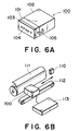
- Fig. 6A shows an example of the recording head, wherein the numeral 101 represents the head substrate illustrated in Fig. 5B; the numeral 102 an ink tank; the numeral 103 an orifice having a plurality of ink emitting orifice; and the numeral 105 an ink supplying pipe.
- the numeral 101 represents the head substrate illustrated in Fig. 5B
- the numeral 102 an ink tank
- the numeral 103 an orifice having a plurality of ink emitting orifice
- the numeral 105 an ink supplying pipe.
- other types of recording heads i.e., one that is fixed to the body of the recording device, one that is an interchangeable chip type enabling an electrical connection with the body of the device when installed into the body of the device and enabling the ink supply from the body of the device, or one that is a cartridge type incorporating the ink tank integrally into the recording head can be effectively applied to the present invention.
- Fig. 6B shows a recording device, wherein the numeral 11 represents a recording medium; the numeral 112 head carrying means; and the numeral 113 a control circuit.
- projection recovery means 110 or preliminary supplemental means for the recording head 100 can be supplemented to stabilize more the advantage of the present invention. More concretely, capping means, pressing or absorbing means, preliminary heating means constituted by either the electro-thermal converter, other thermal elements or the combination thereof, and preliminary emission means for use of other emitting excepting the recording can be supplemented to the recording head.
- one single recording head corresponding to a single color ink or a plurality of recording heads corresponding to a plurality of inks which reveal different recording colors and densities can be employed.
- the recording device can be realized not only by employing a single recording head having a single color mode which reveals a single principal color, like black, but also by employing either a recording head integrally incorporated into the body of the device or a combination of a plurality of the recording head.
- the present invention is effectively applied to the recording device incorporating at least one recording mode selected from a plural color mode revealing different multiple colors and a full color mode realized by mixing multiple colors.
- the ink is not restricted to be liquid but can be utilized the ink which stays solid less than a room temperature and softens or becomes liquidized at the room temperature.
- the ink can be also utilized which is liquidized when applied a recording signal because the ink utilized under an ink-jet system is usually controlled in temperature into a range of 30°C to 70°C to keep the viscosity in a stabilized emission range.
- the ink which stays normally as it is a solid state and a liquid state when heated, can be utilized in order to positively have the heat elevation energy utilized as the energy to change the ink from a solid state to a liquid state or in order to prevent evaporation of the ink.
- the present invention is applicable in case that is utilized the ink liquidized when applied heat energy such that liquid state ink is projected when a recording signal accompanying heat energy is applied solid state ink or that liquid state ink is solidified when it reaches to a recording medium.
- Examples are a video signal output terminal for information processing devices such as computers, a copier in combination with readers, and a facsimile device having a transceiver function.
- the present invention provides both the N type N well diffusion layer and the P type P well diffusion layer in the N type epitaxial layer which is usually utilized to form the bipolar NPN transistor and incorporates the PMOS and NMOS transistors into the N well layer and the P well layer, respectively, the formation regions of both MOS transistors can be approximately equal each other thereby improving the array density of the shift register, the latch circuit and the logic gate.
- the array density of functional elements for a driving system can be well improved to cope with the multi-bit trend of the electro-thermal converter element accompanying high recording density.
Landscapes
- Particle Formation And Scattering Control In Inkjet Printers (AREA)
- Metal-Oxide And Bipolar Metal-Oxide Semiconductor Integrated Circuits (AREA)
Applications Claiming Priority (3)
| Application Number | Priority Date | Filing Date | Title |
|---|---|---|---|
| JP348483/92 | 1992-12-28 | ||
| JP34848392 | 1992-12-28 | ||
| JP34848392A JP3222593B2 (ja) | 1992-12-28 | 1992-12-28 | インクジェット記録ヘッドおよびインクジェット記録ヘッド用モノリシック集積回路 |
Publications (3)
| Publication Number | Publication Date |
|---|---|
| EP0605211A2 true EP0605211A2 (fr) | 1994-07-06 |
| EP0605211A3 EP0605211A3 (fr) | 1994-12-21 |
| EP0605211B1 EP0605211B1 (fr) | 1999-10-27 |
Family
ID=18397319
Family Applications (1)
| Application Number | Title | Priority Date | Filing Date |
|---|---|---|---|
| EP93310485A Expired - Lifetime EP0605211B1 (fr) | 1992-12-28 | 1993-12-23 | Tête d'enregistrement du type à jet d'encre et circuit intégré monolithique approprié |
Country Status (5)
| Country | Link |
|---|---|
| US (1) | US5602576A (fr) |
| EP (1) | EP0605211B1 (fr) |
| JP (1) | JP3222593B2 (fr) |
| AT (1) | ATE186017T1 (fr) |
| DE (1) | DE69326877T2 (fr) |
Cited By (4)
| Publication number | Priority date | Publication date | Assignee | Title |
|---|---|---|---|---|
| EP0771656A3 (fr) * | 1995-10-30 | 1997-11-05 | Eastman Kodak Company | Dispersion des buses pour réduire l'interaction électrostatique entre gouttelettes imprimées simultanément |
| EP0816082A3 (fr) * | 1996-06-26 | 1999-06-02 | Canon Kabushiki Kaisha | Tête d'enregistrement et appareil d'enregistrement l'utilisant |
| US7380339B2 (en) * | 1998-10-16 | 2008-06-03 | Silverbrook Research Pty Ltd | Method of manufacturing a printhead wafer etched from opposing sides |
| CN102026815A (zh) * | 2008-05-15 | 2011-04-20 | 惠普开发有限公司 | 柔性电路密封 |
Families Citing this family (36)
| Publication number | Priority date | Publication date | Assignee | Title |
|---|---|---|---|---|
| US5850242A (en) * | 1995-03-07 | 1998-12-15 | Canon Kabushiki Kaisha | Recording head and recording apparatus and method of manufacturing same |
| JP3400181B2 (ja) * | 1995-04-25 | 2003-04-28 | ローム株式会社 | 半導体装置およびその製造方法 |
| JP3542460B2 (ja) * | 1996-06-07 | 2004-07-14 | キヤノン株式会社 | 液体吐出方法及び液体吐出装置 |
| DE69724875T2 (de) * | 1996-06-26 | 2004-07-22 | Canon K.K. | Tintenstrahlaufzeichnungskopf und Tintenstrahlaufzeichnungsapparat |
| US6773092B1 (en) | 1996-07-05 | 2004-08-10 | Aya Yoshihira | Liquid discharging head and liquid discharging device |
| JP3403008B2 (ja) * | 1996-07-05 | 2003-05-06 | キヤノン株式会社 | 液体吐出ヘッドおよびそれを用いたヘッドカートリッジと記録装置 |
| US6070970A (en) * | 1996-07-11 | 2000-06-06 | Canon Kabushiki Kaisha | Liquid discharging method and liquid-discharge head, ink-jet recording method and head for ink-jet recording method |
| JP3372765B2 (ja) | 1996-07-12 | 2003-02-04 | キヤノン株式会社 | 液体吐出ヘッド、ヘッドカートリッジ、液体吐出装置、記録システム、ヘッドキット、および液体吐出ヘッドの製造方法 |
| JP3403009B2 (ja) * | 1996-07-12 | 2003-05-06 | キヤノン株式会社 | 可動部材の変位と気泡成長を伴う液体吐出方法、該吐出方法に用いられる液体吐出ヘッド、ヘッドカートリッジ及びこれらを用いた液体吐出装置 |
| JP3403010B2 (ja) | 1996-07-12 | 2003-05-06 | キヤノン株式会社 | 液体吐出ヘッド |
| JPH1024584A (ja) | 1996-07-12 | 1998-01-27 | Canon Inc | 液体吐出ヘッドカートリッジおよび液体吐出装置 |
| JP3372827B2 (ja) | 1996-07-12 | 2003-02-04 | キヤノン株式会社 | 液体吐出方法及び液体吐出ヘッド並びに該吐出ヘッドを用いたヘッドカートリッジ及び液体吐出装置 |
| JPH10119314A (ja) | 1996-08-30 | 1998-05-12 | Canon Inc | 液体吐出ヘッドユニットの結合方法、液体吐出ヘッドユニットおよび液体吐出カートリッジ |
| US6396109B1 (en) * | 1996-12-06 | 2002-05-28 | Texas Instruments Incorporated | Isolated NMOS transistor fabricated in a digital BiCMOS process |
| US6183067B1 (en) * | 1997-01-21 | 2001-02-06 | Agilent Technologies | Inkjet printhead and fabrication method for integrating an actuator and firing chamber |
| US6331043B1 (en) | 1997-06-06 | 2001-12-18 | Canon Kabushiki Kaisha | Liquid discharging method, a liquid discharge head, and a liquid discharger apparatus |
| JP3416465B2 (ja) | 1997-06-06 | 2003-06-16 | キヤノン株式会社 | 液体吐出方法及び液体吐出ヘッド |
| JP3524340B2 (ja) | 1997-08-26 | 2004-05-10 | キヤノン株式会社 | 液体吐出ヘッド |
| JPH11227209A (ja) | 1997-12-05 | 1999-08-24 | Canon Inc | 液体吐出ヘッド、ヘッドカートリッジおよび液体吐出装置 |
| JPH11227210A (ja) | 1997-12-05 | 1999-08-24 | Canon Inc | 液体吐出ヘッド、該ヘッドの製造方法、ヘッドカートリッジおよび液体吐出装置 |
| JP2000198199A (ja) | 1997-12-05 | 2000-07-18 | Canon Inc | 液体吐出ヘッドおよびヘッドカートリッジおよび液体吐出装置および液体吐出ヘッドの製造方法 |
| US7101099B1 (en) | 1998-08-19 | 2006-09-05 | Canon Kabushiki Kaisha | Printing head, head cartridge having printing head, printing apparatus using printing head, and printing head substrate |
| US6902255B1 (en) | 1998-10-16 | 2005-06-07 | Silverbrook Research Pty Ltd | Inkjet printers |
| JP2000141660A (ja) | 1998-11-11 | 2000-05-23 | Canon Inc | 記録へッド及びその記録へッドを用いた記録装置 |
| IT1310099B1 (it) * | 1999-07-12 | 2002-02-11 | Olivetti Lexikon Spa | Testina di stampa monolitica e relativo processo di fabbricazione. |
| IT1320599B1 (it) * | 2000-08-23 | 2003-12-10 | Olivetti Lexikon Spa | Testina di stampa monolitica con scanalatura autoallineata e relativoprocesso di fabbricazione. |
| US6825543B2 (en) | 2000-12-28 | 2004-11-30 | Canon Kabushiki Kaisha | Semiconductor device, method for manufacturing the same, and liquid jet apparatus |
| DE60108838T2 (de) * | 2000-12-29 | 2006-05-04 | Eastman Kodak Co. | Integrierter cmos/mems-tintenstrahldruckkopf mit seitenstromdüsen-architektur auf siliciumbasis und verfahren zu dessen herstellung |
| US6502925B2 (en) | 2001-02-22 | 2003-01-07 | Eastman Kodak Company | CMOS/MEMS integrated ink jet print head and method of operating same |
| US6382782B1 (en) * | 2000-12-29 | 2002-05-07 | Eastman Kodak Company | CMOS/MEMS integrated ink jet print head with oxide based lateral flow nozzle architecture and method of forming same |
| US6800902B2 (en) | 2001-02-16 | 2004-10-05 | Canon Kabushiki Kaisha | Semiconductor device, method of manufacturing the same and liquid jet apparatus |
| US6491385B2 (en) * | 2001-02-22 | 2002-12-10 | Eastman Kodak Company | CMOS/MEMS integrated ink jet print head with elongated bore and method of forming same |
| JP4035385B2 (ja) * | 2002-06-19 | 2008-01-23 | キヤノン株式会社 | 駆動回路、記録ヘッド及び記録装置 |
| KR100731352B1 (ko) * | 2004-01-28 | 2007-06-21 | 삼성전자주식회사 | 잉크젯 프린터의 헤드칩 |
| JP4027331B2 (ja) * | 2004-02-27 | 2007-12-26 | ローム株式会社 | ドライバ装置及びプリントヘッド |
| KR100884427B1 (ko) * | 2004-04-02 | 2009-02-19 | 실버브룩 리서치 피티와이 리미티드 | 내부 또는 그 상면에 배치된 부호화된 데이터를 가지는표면 |
Family Cites Families (17)
| Publication number | Priority date | Publication date | Assignee | Title |
|---|---|---|---|---|
| CA1127227A (fr) * | 1977-10-03 | 1982-07-06 | Ichiro Endo | Procede d'enregistrement a jet liquide et appareil d'enregistrement |
| JPS5936879B2 (ja) * | 1977-10-14 | 1984-09-06 | キヤノン株式会社 | 熱転写記録用媒体 |
| US4330787A (en) * | 1978-10-31 | 1982-05-18 | Canon Kabushiki Kaisha | Liquid jet recording device |
| US4345262A (en) * | 1979-02-19 | 1982-08-17 | Canon Kabushiki Kaisha | Ink jet recording method |
| US4463359A (en) * | 1979-04-02 | 1984-07-31 | Canon Kabushiki Kaisha | Droplet generating method and apparatus thereof |
| US4313124A (en) * | 1979-05-18 | 1982-01-26 | Canon Kabushiki Kaisha | Liquid jet recording process and liquid jet recording head |
| US4558333A (en) * | 1981-07-09 | 1985-12-10 | Canon Kabushiki Kaisha | Liquid jet recording head |
| JPS59123670A (ja) * | 1982-12-28 | 1984-07-17 | Canon Inc | インクジエツトヘツド |
| JPS59138461A (ja) * | 1983-01-28 | 1984-08-08 | Canon Inc | 液体噴射記録装置 |
| JPS6071260A (ja) * | 1983-09-28 | 1985-04-23 | Erumu:Kk | 記録装置 |
| US5175565A (en) * | 1988-07-26 | 1992-12-29 | Canon Kabushiki Kaisha | Ink jet substrate including plural temperature sensors and heaters |
| US5055859A (en) * | 1988-11-16 | 1991-10-08 | Casio Computer Co., Ltd. | Integrated thermal printhead and driving circuit |
| EP0378439B1 (fr) * | 1989-01-13 | 1995-01-04 | Canon Kabushiki Kaisha | Tête d'enregistrement |
| CA2025559C (fr) * | 1989-09-18 | 1998-09-15 | Masaaki Izumida | Tete d'enregistrement a jet liquide et appareil d'enregistrement a jet liquide comportant cette tete |
| US5045870A (en) * | 1990-04-02 | 1991-09-03 | International Business Machines Corporation | Thermal ink drop on demand devices on a single chip with vertical integration of driver device |
| US5214450A (en) * | 1990-06-15 | 1993-05-25 | Canon Kabushiki Kaisha | Thermal ink jet recording apparatus using a grouped transducer drive |
| CA2075097C (fr) * | 1991-08-02 | 2000-03-28 | Hiroyuki Ishinaga | Appareil d'enregistrement, tete d'enregistrement et substrat connexe |
-
1992
- 1992-12-28 JP JP34848392A patent/JP3222593B2/ja not_active Expired - Fee Related
-
1993
- 1993-12-23 EP EP93310485A patent/EP0605211B1/fr not_active Expired - Lifetime
- 1993-12-23 DE DE69326877T patent/DE69326877T2/de not_active Expired - Fee Related
- 1993-12-23 AT AT93310485T patent/ATE186017T1/de not_active IP Right Cessation
-
1996
- 1996-04-15 US US08/632,727 patent/US5602576A/en not_active Expired - Fee Related
Cited By (8)
| Publication number | Priority date | Publication date | Assignee | Title |
|---|---|---|---|---|
| EP0771656A3 (fr) * | 1995-10-30 | 1997-11-05 | Eastman Kodak Company | Dispersion des buses pour réduire l'interaction électrostatique entre gouttelettes imprimées simultanément |
| US6126846A (en) * | 1995-10-30 | 2000-10-03 | Eastman Kodak Company | Print head constructions for reduced electrostatic interaction between printed droplets |
| EP0816082A3 (fr) * | 1996-06-26 | 1999-06-02 | Canon Kabushiki Kaisha | Tête d'enregistrement et appareil d'enregistrement l'utilisant |
| US6302504B1 (en) | 1996-06-26 | 2001-10-16 | Canon Kabushiki Kaisha | Recording head and recording apparatus using the same |
| US7380339B2 (en) * | 1998-10-16 | 2008-06-03 | Silverbrook Research Pty Ltd | Method of manufacturing a printhead wafer etched from opposing sides |
| US7537314B2 (en) | 1998-10-16 | 2009-05-26 | Silverbrook Research Pty Ltd | Inkjet printhead having nozzle arrangements with ink spreading prevention rims |
| US7771025B2 (en) | 1998-10-16 | 2010-08-10 | Silverbrook Research Pty Ltd | Inkjet printhead having plural nozzle arrangements grouped in pods |
| CN102026815A (zh) * | 2008-05-15 | 2011-04-20 | 惠普开发有限公司 | 柔性电路密封 |
Also Published As
| Publication number | Publication date |
|---|---|
| JPH06198885A (ja) | 1994-07-19 |
| EP0605211B1 (fr) | 1999-10-27 |
| US5602576A (en) | 1997-02-11 |
| ATE186017T1 (de) | 1999-11-15 |
| EP0605211A3 (fr) | 1994-12-21 |
| DE69326877D1 (de) | 1999-12-02 |
| JP3222593B2 (ja) | 2001-10-29 |
| DE69326877T2 (de) | 2000-04-27 |
Similar Documents
| Publication | Publication Date | Title |
|---|---|---|
| US5602576A (en) | Ink-jet type recording head and monolithic integrated circuit suitable therfor | |
| US6439690B2 (en) | Element substrate having connecting wiring between heat generating resistor elements and ink jet recording apparatus | |
| EP1122071B1 (fr) | Plaquette semiconductrice pour tête d' imprimante | |
| US6019457A (en) | Ink jet print device and print head or print apparatus using the same | |
| KR100442515B1 (ko) | 프린트 헤드와 이 프린트 헤드를 사용하는 인쇄 장치 | |
| US6137509A (en) | Recording apparatus having a substrate for a recording head and method of producing the same | |
| US6126277A (en) | Non-kogating, low turn on energy thin film structure for very low drop volume thermal ink jet pens | |
| US6523922B2 (en) | Printhead as well as printing apparatus comprising such printhead | |
| US6474788B1 (en) | Substrate for use of ink jet head, ink jet head, ink jet cartridge, and ink jet recording apparatus | |
| EP1080903B1 (fr) | Retours communs à la base multi-bornes pour tête d'impression à jet d'encre | |
| US6782621B2 (en) | Method of fabricating a fluid ejector | |
| CA2545241C (fr) | Dispositif d'ejection de microfluide presentant des circuits logiques et pilotes | |
| CN114434968A (zh) | 晶圆结构 | |
| EP0792745A2 (fr) | Tête d'enregistrement à jet d'encre | |
| JPH08108538A (ja) | 記録ヘッド及び該記録ヘッドを用いた記録装置 | |
| JPH08300656A (ja) | インクジェット記録ヘッド、インクジェット記録装置および情報処理システム | |
| JPH0911468A (ja) | インクジェット記録ヘッド用基体、インクジェット記録ヘッド、インクジェット記録装置および情報処理システム | |
| JPH0776081A (ja) | 記録ヘッド用基体、記録ヘッドおよびインクジェット記録装置 |
Legal Events
| Date | Code | Title | Description |
|---|---|---|---|
| PUAI | Public reference made under article 153(3) epc to a published international application that has entered the european phase |
Free format text: ORIGINAL CODE: 0009012 |
|
| AK | Designated contracting states |
Kind code of ref document: A2 Designated state(s): AT BE CH DE DK ES FR GB GR IE IT LI LU NL PT SE |
|
| PUAL | Search report despatched |
Free format text: ORIGINAL CODE: 0009013 |
|
| AK | Designated contracting states |
Kind code of ref document: A3 Designated state(s): AT BE CH DE DK ES FR GB GR IE IT LI LU NL PT SE |
|
| 17P | Request for examination filed |
Effective date: 19950502 |
|
| 17Q | First examination report despatched |
Effective date: 19960610 |
|
| GRAG | Despatch of communication of intention to grant |
Free format text: ORIGINAL CODE: EPIDOS AGRA |
|
| GRAG | Despatch of communication of intention to grant |
Free format text: ORIGINAL CODE: EPIDOS AGRA |
|
| GRAG | Despatch of communication of intention to grant |
Free format text: ORIGINAL CODE: EPIDOS AGRA |
|
| GRAH | Despatch of communication of intention to grant a patent |
Free format text: ORIGINAL CODE: EPIDOS IGRA |
|
| RIN1 | Information on inventor provided before grant (corrected) |
Inventor name: MISUMI, YOSHINORI, C/O CANON KABUSHIKI KAISHA Inventor name: IZUMIDA, MASAAKI, C/O CANON KABUSHIKI KAISHA Inventor name: MARU, HIROYUKI, C/O CANON KABUSHIKI KAISHA Inventor name: ISHINAGA, HIROYUKI, C/O CANON KABUSHIKI KAISHA Inventor name: FURUKAWA, TATSUO, C/O CANON KABUSHIKI KAISHA Inventor name: SHIMODA, JUNJI, C/O CANON KABUSHIKI KAISHA Inventor name: MUROOKA, FUMIO, C/O CANON KABUSHIKI KAISHA |
|
| GRAH | Despatch of communication of intention to grant a patent |
Free format text: ORIGINAL CODE: EPIDOS IGRA |
|
| GRAA | (expected) grant |
Free format text: ORIGINAL CODE: 0009210 |
|
| AK | Designated contracting states |
Kind code of ref document: B1 Designated state(s): AT BE CH DE DK ES FR GB GR IE IT LI LU NL PT SE |
|
| PG25 | Lapsed in a contracting state [announced via postgrant information from national office to epo] |
Ref country code: SE Free format text: THE PATENT HAS BEEN ANNULLED BY A DECISION OF A NATIONAL AUTHORITY Effective date: 19991027 Ref country code: NL Free format text: LAPSE BECAUSE OF FAILURE TO SUBMIT A TRANSLATION OF THE DESCRIPTION OR TO PAY THE FEE WITHIN THE PRESCRIBED TIME-LIMIT Effective date: 19991027 Ref country code: LI Free format text: LAPSE BECAUSE OF FAILURE TO SUBMIT A TRANSLATION OF THE DESCRIPTION OR TO PAY THE FEE WITHIN THE PRESCRIBED TIME-LIMIT Effective date: 19991027 Ref country code: GR Free format text: LAPSE BECAUSE OF NON-PAYMENT OF DUE FEES Effective date: 19991027 Ref country code: ES Free format text: THE PATENT HAS BEEN ANNULLED BY A DECISION OF A NATIONAL AUTHORITY Effective date: 19991027 Ref country code: CH Free format text: LAPSE BECAUSE OF FAILURE TO SUBMIT A TRANSLATION OF THE DESCRIPTION OR TO PAY THE FEE WITHIN THE PRESCRIBED TIME-LIMIT Effective date: 19991027 Ref country code: BE Free format text: LAPSE BECAUSE OF FAILURE TO SUBMIT A TRANSLATION OF THE DESCRIPTION OR TO PAY THE FEE WITHIN THE PRESCRIBED TIME-LIMIT Effective date: 19991027 Ref country code: AT Free format text: LAPSE BECAUSE OF FAILURE TO SUBMIT A TRANSLATION OF THE DESCRIPTION OR TO PAY THE FEE WITHIN THE PRESCRIBED TIME-LIMIT Effective date: 19991027 |
|
| REF | Corresponds to: |
Ref document number: 186017 Country of ref document: AT Date of ref document: 19991115 Kind code of ref document: T |
|
| REG | Reference to a national code |
Ref country code: CH Ref legal event code: EP |
|
| REF | Corresponds to: |
Ref document number: 69326877 Country of ref document: DE Date of ref document: 19991202 |
|
| PG25 | Lapsed in a contracting state [announced via postgrant information from national office to epo] |
Ref country code: LU Free format text: LAPSE BECAUSE OF NON-PAYMENT OF DUE FEES Effective date: 19991223 |
|
| PG25 | Lapsed in a contracting state [announced via postgrant information from national office to epo] |
Ref country code: IE Free format text: LAPSE BECAUSE OF NON-PAYMENT OF DUE FEES Effective date: 19991227 |
|
| ET | Fr: translation filed | ||
| ITF | It: translation for a ep patent filed | ||
| REG | Reference to a national code |
Ref country code: IE Ref legal event code: FG4D |
|
| PG25 | Lapsed in a contracting state [announced via postgrant information from national office to epo] |
Ref country code: PT Free format text: LAPSE BECAUSE OF FAILURE TO SUBMIT A TRANSLATION OF THE DESCRIPTION OR TO PAY THE FEE WITHIN THE PRESCRIBED TIME-LIMIT Effective date: 20000127 Ref country code: DK Free format text: LAPSE BECAUSE OF FAILURE TO SUBMIT A TRANSLATION OF THE DESCRIPTION OR TO PAY THE FEE WITHIN THE PRESCRIBED TIME-LIMIT Effective date: 20000127 |
|
| NLV1 | Nl: lapsed or annulled due to failure to fulfill the requirements of art. 29p and 29m of the patents act | ||
| REG | Reference to a national code |
Ref country code: CH Ref legal event code: PL |
|
| PLBE | No opposition filed within time limit |
Free format text: ORIGINAL CODE: 0009261 |
|
| STAA | Information on the status of an ep patent application or granted ep patent |
Free format text: STATUS: NO OPPOSITION FILED WITHIN TIME LIMIT |
|
| REG | Reference to a national code |
Ref country code: IE Ref legal event code: MM4A |
|
| 26N | No opposition filed | ||
| REG | Reference to a national code |
Ref country code: GB Ref legal event code: IF02 |
|
| PGFP | Annual fee paid to national office [announced via postgrant information from national office to epo] |
Ref country code: IT Payment date: 20071218 Year of fee payment: 15 |
|
| PGFP | Annual fee paid to national office [announced via postgrant information from national office to epo] |
Ref country code: GB Payment date: 20071228 Year of fee payment: 15 |
|
| PGFP | Annual fee paid to national office [announced via postgrant information from national office to epo] |
Ref country code: DE Payment date: 20071231 Year of fee payment: 15 |
|
| PGFP | Annual fee paid to national office [announced via postgrant information from national office to epo] |
Ref country code: FR Payment date: 20071220 Year of fee payment: 15 |
|
| GBPC | Gb: european patent ceased through non-payment of renewal fee |
Effective date: 20081223 |
|
| REG | Reference to a national code |
Ref country code: FR Ref legal event code: ST Effective date: 20090831 |
|
| PG25 | Lapsed in a contracting state [announced via postgrant information from national office to epo] |
Ref country code: DE Free format text: LAPSE BECAUSE OF NON-PAYMENT OF DUE FEES Effective date: 20090701 |
|
| PG25 | Lapsed in a contracting state [announced via postgrant information from national office to epo] |
Ref country code: GB Free format text: LAPSE BECAUSE OF NON-PAYMENT OF DUE FEES Effective date: 20081223 |
|
| PG25 | Lapsed in a contracting state [announced via postgrant information from national office to epo] |
Ref country code: FR Free format text: LAPSE BECAUSE OF NON-PAYMENT OF DUE FEES Effective date: 20081231 |
|
| PG25 | Lapsed in a contracting state [announced via postgrant information from national office to epo] |
Ref country code: IT Free format text: LAPSE BECAUSE OF NON-PAYMENT OF DUE FEES Effective date: 20081223 |