EP0605929A1 - Vorrichtung zur optischen Abtastung einer Fläche - Google Patents
Vorrichtung zur optischen Abtastung einer Fläche Download PDFInfo
- Publication number
- EP0605929A1 EP0605929A1 EP93203700A EP93203700A EP0605929A1 EP 0605929 A1 EP0605929 A1 EP 0605929A1 EP 93203700 A EP93203700 A EP 93203700A EP 93203700 A EP93203700 A EP 93203700A EP 0605929 A1 EP0605929 A1 EP 0605929A1
- Authority
- EP
- European Patent Office
- Prior art keywords
- grating
- radiation
- grating structure
- monitor
- radiation source
- Prior art date
- Legal status (The legal status is an assumption and is not a legal conclusion. Google has not performed a legal analysis and makes no representation as to the accuracy of the status listed.)
- Granted
Links
Images
Classifications
-
- G—PHYSICS
- G11—INFORMATION STORAGE
- G11B—INFORMATION STORAGE BASED ON RELATIVE MOVEMENT BETWEEN RECORD CARRIER AND TRANSDUCER
- G11B7/00—Recording or reproducing by optical means, e.g. recording using a thermal beam of optical radiation by modifying optical properties or the physical structure, reproducing using an optical beam at lower power by sensing optical properties; Record carriers therefor
- G11B7/12—Heads, e.g. forming of the optical beam spot or modulation of the optical beam
- G11B7/125—Optical beam sources therefor, e.g. laser control circuitry specially adapted for optical storage devices; Modulators, e.g. means for controlling the size or intensity of optical spots or optical traces
- G11B7/126—Circuits, methods or arrangements for laser control or stabilisation
-
- G—PHYSICS
- G02—OPTICS
- G02B—OPTICAL ELEMENTS, SYSTEMS OR APPARATUS
- G02B27/00—Optical systems or apparatus not provided for by any of the groups G02B1/00 - G02B26/00, G02B30/00
- G02B27/10—Beam splitting or combining systems
- G02B27/1073—Beam splitting or combining systems characterized by manufacturing or alignment methods
-
- G—PHYSICS
- G02—OPTICS
- G02B—OPTICAL ELEMENTS, SYSTEMS OR APPARATUS
- G02B27/00—Optical systems or apparatus not provided for by any of the groups G02B1/00 - G02B26/00, G02B30/00
- G02B27/10—Beam splitting or combining systems
- G02B27/1086—Beam splitting or combining systems operating by diffraction only
- G02B27/1093—Beam splitting or combining systems operating by diffraction only for use with monochromatic radiation only, e.g. devices for splitting a single laser source
-
- G—PHYSICS
- G11—INFORMATION STORAGE
- G11B—INFORMATION STORAGE BASED ON RELATIVE MOVEMENT BETWEEN RECORD CARRIER AND TRANSDUCER
- G11B7/00—Recording or reproducing by optical means, e.g. recording using a thermal beam of optical radiation by modifying optical properties or the physical structure, reproducing using an optical beam at lower power by sensing optical properties; Record carriers therefor
- G11B7/12—Heads, e.g. forming of the optical beam spot or modulation of the optical beam
- G11B7/135—Means for guiding the beam from the source to the record carrier or from the record carrier to the detector
- G11B7/1353—Diffractive elements, e.g. holograms or gratings
-
- H—ELECTRICITY
- H01—ELECTRIC ELEMENTS
- H01S—DEVICES USING THE PROCESS OF LIGHT AMPLIFICATION BY STIMULATED EMISSION OF RADIATION [LASER] TO AMPLIFY OR GENERATE LIGHT; DEVICES USING STIMULATED EMISSION OF ELECTROMAGNETIC RADIATION IN WAVE RANGES OTHER THAN OPTICAL
- H01S5/00—Semiconductor lasers
- H01S5/02—Structural details or components not essential to laser action
- H01S5/022—Mountings; Housings
- H01S5/02208—Mountings; Housings characterised by the shape of the housings
- H01S5/02212—Can-type, e.g. TO-CAN housings with emission along or parallel to symmetry axis
-
- H—ELECTRICITY
- H01—ELECTRIC ELEMENTS
- H01S—DEVICES USING THE PROCESS OF LIGHT AMPLIFICATION BY STIMULATED EMISSION OF RADIATION [LASER] TO AMPLIFY OR GENERATE LIGHT; DEVICES USING STIMULATED EMISSION OF ELECTROMAGNETIC RADIATION IN WAVE RANGES OTHER THAN OPTICAL
- H01S5/00—Semiconductor lasers
- H01S5/02—Structural details or components not essential to laser action
- H01S5/022—Mountings; Housings
- H01S5/0225—Out-coupling of light
- H01S5/02257—Out-coupling of light using windows, e.g. specially adapted for back-reflecting light to a detector inside the housing
-
- H—ELECTRICITY
- H01—ELECTRIC ELEMENTS
- H01S—DEVICES USING THE PROCESS OF LIGHT AMPLIFICATION BY STIMULATED EMISSION OF RADIATION [LASER] TO AMPLIFY OR GENERATE LIGHT; DEVICES USING STIMULATED EMISSION OF ELECTROMAGNETIC RADIATION IN WAVE RANGES OTHER THAN OPTICAL
- H01S5/00—Semiconductor lasers
- H01S5/02—Structural details or components not essential to laser action
- H01S5/022—Mountings; Housings
- H01S5/023—Mount members, e.g. sub-mount members
- H01S5/02325—Mechanically integrated components on mount members or optical micro-benches
-
- H—ELECTRICITY
- H01—ELECTRIC ELEMENTS
- H01S—DEVICES USING THE PROCESS OF LIGHT AMPLIFICATION BY STIMULATED EMISSION OF RADIATION [LASER] TO AMPLIFY OR GENERATE LIGHT; DEVICES USING STIMULATED EMISSION OF ELECTROMAGNETIC RADIATION IN WAVE RANGES OTHER THAN OPTICAL
- H01S5/00—Semiconductor lasers
- H01S5/06—Arrangements for controlling the laser output parameters, e.g. by operating on the active medium
- H01S5/068—Stabilisation of laser output parameters
- H01S5/0683—Stabilisation of laser output parameters by monitoring the optical output parameters
Definitions
- the invention relates to a device for optically scanning a surface, which device comprises a radiation source-detection unit and focusing means for focusing radiation supplied by the radiation source-detection unit on the surface, said radiation source-detection unit comprising a radiation source for supplying a radiation beam, a grating having a first grating structure for forming at least a deflected sub-beam from the radiation beam supplied by the radiation source or from a beam reflected by the surface, a radiation-sensitive detection system for converting radiation reflected by the surface into electric signals, means for forming a monitor beam from the beam supplied by the radiation source, and a monitor detector for converting the monitor beam into an electric signal for controlling the radiation source.
- the invention also relates to a radiation source-detection unit for use in such a device.
- a device of the type described in the opening paragraph is known from European Patent Application no. 0 372 629 (PHN 12.753).
- This device can be used for scanning a record carrier by means of a radiation beam.
- a three-spot grating is placed in the radiation beam of the device. In transmission, this grating forms two first-order diffracted sub-beams from the radiation beam. Together with the on-going non-deflected main beam, the two sub-beams are focused by an objective system to three spots on the record carrier.
- the main spot formed by the main beam is used for writing or reading information in the tracks of the record carrier.
- the side spots formed by the side beams are used for generating a tracking signal with which a circuit is controlled which keeps the main spot on the track to be scanned.
- the write power When information is being written in the record carrier, it is desirable that the power in the main beam is maintained accurately at a given value, referred to as the write power.
- a reflector is arranged around the grating, which reflector reflects a part of the radiation from the radiation source falling outside the grating, referred to as the border radiation, to a monitor detector arranged beside the radiation source.
- the signal from the monitor detector is subsequently used for controlling the power supplied by the radiation source.
- a drawback is that the ratio between the border radiation power and the main beam power is dependent on the radiation source used, so that the monitor detector must be calibrated for each device.
- the device according to the invention is characterized in that the monitor beam-forming means are constituted by a second grating structure in the grating and in that the monitor beam consists of radiation reflected by the grating.
- the monitor beam is formed from the same part of the radiation beam as the part from which the grating forms the main beam. Consequently, the power in the monitor beam is a fixed fraction of the power in the main beam.
- the output signal of the monitor detector is then a direct measure of the power in the main beam so that it is no longer necessary to calibrate.
- the direction of this beam can be made approximately equal to the direction of the main beam to be captured by the radiation-sensitive detection system. This provides the possibility of integrating the monitor detector with the detection system so that the device can be made in a simpler manner and at lower cost.
- An embodiment of the device according to the invention is characterized in that the first grating structure has a grating groove depth which is approximately equal to half the wavelength of the radiation and in that the second grating structure is blazed for preferential diffraction in the direction of the monitor detector.
- the invention is based on the recognition that the reflection of the second grating structure is still sufficiently large to obtain sufficient radiation on the monitor diode, provided that it is ensured, by means of an operation referred to as "blazing" of the second grating structure, that this radiation is concentrated as much as possible into a beam of one diffraction order.
- the modified grating also forms beams which are diffracted by the two grating structures in a first or a higher order. Such beams only cause loss of radiation.
- This radiation is reduced in a device according to the invention which is characterized in that the grating grooves of the first grating structure are substantially perpendicular to the grating grooves of the second grating structure. The deviation from perpendicular is preferably smaller than 30°. The combination of this measure with said choice of the depth of the grating grooves and blazing of the first and second grating structures results in an even more effective suppression of these beams.
- a particular embodiment of the device according to the invention is characterized in that the second grating structure has optical power. Due to the optical power, the monitor beam is focused on the monitor detector so that the monitor detector may be small.
- the first grating structure is a linear grating structure for forming a non-deflected main beam and two side beams deflected in opposite directions from the radiation beam supplied by the source, and in that the detection system has a separate detector for each of the three beams reflected by the surface.
- the first grating structure generates, in transmission, the two sub-beams which, in the form of two side beams at both sides of the main beam, are formed by the objective system to two side spots at both sides of the main spot.
- the radiation reflected by these side spots is detected by means of the detection system in order to derive a signal indicating the extent to which the main spot correctly tracks the track to be scanned.
- An embodiment of the device according to the invention is characterized in that the first grating structure is adapted to deflect a radiation beam reflected by the surface towards the detection system and to deform the deflected beam in such a way that a focus error signal can be derived therefrom by means of the detection system.
- a special grating structure can introduce astigmatism into the deflected beam so that a focus error signal in accordance with the astigmatic method can be generated with this beam.
- Two sub-beams, from which a focus error signal can also be generated by means of the Foucault method, can be generated with a different grating structure.
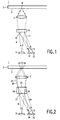
- Fig. 1 shows a device for scanning an optical record carrier 1, a part of which is shown in a cross-section.
- the record carrier comprises a substrate 2 provided with a reflecting recording layer 3.
- the recording layer is scanned from the air side; it is, however, preferred to scan the recording layer through the then transparent substrate.
- the information on the recording layer is ordered in tracks which are not shown in the Figure.
- a radiation source 5 for example a semiconductor laser, supplies a radiation beam 6 which is focused by an objective system 7 on the recording layer 3 to form a spot 8 for scanning the recording layer. It must be possible to detect the beam reflected by the recording layer and modulated by the information structure, for which purpose this beam must be separated from the on-going beam.
- the device can be provided in known manner with a transparent plate 9 provided with a grating 10 which is dimensioned in such a way that it passes the reflected beam substantially in a given diffraction order.
- the sub-beam thus formed and deflected is captured by a detection system 12 which converts the sub-beam into one or more electric signals, for example an information signal, a tracking error signal and a focus error signal.
- the tracking error signal and the focus error signal are used in servocircuits (not shown) for controlling the position of the spot 8 in such a way that it remains in the recording plane and continues to track the track to be scanned.
- the grating 10 may have a first grating structure with straight grating grooves. Due to a special curvature of the grating grooves, inter alia known from United States Patent no. 4,358,200, the deflected sub-beam 11 can be made astigmatic. If the detection system 12 has four detectors arranged in quadrants, onto whose centre the sub-beam is directed, a focus error signal can be derived from the output signals of the four detectors in accordance with the astigmatic method as described in said United States Patent. In another embodiment, known from United States Patent no.
- the grating 10 has two sub-gratings at both sides of a dividing line, in which each sub-grating has a series of substantially parallel grating grooves, while the grating grooves of the first sub-grating extend at a first angle and those of the second sub-grating extend at a second, for example equally large but opposite angle to the dividing line.
- the two sub-gratings of such a Foucault grating each form a sub-beam from the radiation reflected by the recording plane. These sub-beams, which have different directions, are incident on separate detector pairs of the detection system. The output signals of these detectors are processed to a focus error signal. This detection method is known as the Foucault method.
- the structure of the grating 10 is modified in accordance with the invention in such a way that the part of the on-going radiation beam 6 reflected by the grating is deflected into a diffracted monitor beam 13.
- a monitor detector 14 converts this beam into a control signal which is used for maintaining the power supplied by the radiation source at a desired value.
- the new grating is composed of a first grating structure for deflecting and possibly diffracting the signal and servobeam 11 into a shape suitable for focus detection, on which first grating structure a second grating structure for forming the monitor beam 13 is superimposed.
- the grating grooves of the second grating structure may be curved to give the structure an optical power.
- a converging monitor beam 13 is formed from the diverging radiation beam 6.
- the average angle between the grating grooves of the first and second grating structures is preferably approximately 90° in order to reduce the interference between the two grating structures and to enhance the possibility of manufacturing the grating.
- the monitor detector 14 is arranged in front of or behind the radiation source 5, viewed in a direction perpendicular to the plane of the drawing in Fig. 1.
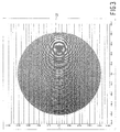
- Fig. 2 shows another embodiment of the device according to the invention.
- the radiation beam 6 from the radiation source 5 is split into a non-deflected main beam 20 and two deflected side beams 21, 22 by a grating 17 arranged on a transparent plate 18.
- the grating 17 has a first grating structure, which is known as a three-spot grating, having substantially equidistant, straight grating grooves.
- the objective system 7 focuses the main beam 20 and side beams 21, 22 formed by this grating structure to a main spot 8 and two side spots 23, 24, respectively, on the recording layer 3.
- a second grating 25 deflecting a substantial part of the radiation reflected by the recording layer as beam 26 to a signal and servodetection system 12 is arranged on the plate 18.
- This second grating 25 may have approximately the same grating structure as the first grating structure in the grating 10 of Fig. 1.
- An information signal as well as a focus error signal can be derived in accordance with either the astigmatic or the Foucault method from the signals supplied by the detection system 12.
- Fig. 2 only shows the deflected reflected main beam 26.
- the grating 25 also deflects the reflected side beams 21 and 22 towards the detection system.
- This system comprises two extra detectors for converting the reflected and deflected side beam radiation into electric signals from which a tracking error signal can be derived.
- the grating 17 in the device shown in Fig. 2 is modified in such a way that the reflected part of the radiation beam is deflected into a monitor beam 13.
- the power in the monitor beam is proportional to the power generated by the radiation source.
- the monitor beam is incident on a monitor detector 14 which converts the incident radiation into an electric signal for controlling the radiation power of the radiation source 5.
- the modification of the grating consists of combining the first grating structure with a second grating structure.
- the second grating structure comprises a collection of grating grooves which may be curved. The curvature gives the grating structure an optical power so that the monitor beam 13 is a converging beam.
- the grating grooves of the first grating structure preferably extend in a direction which is perpendicular to the average direction of the grating grooves of the second grating structure.
- the side beams 21, 22 are then substantially deflected in a direction perpendicular to the plane of the drawing.
- the distances between the side spots 23, 24 and the main spot 8 on the recording layer 3 will therefore be larger in the direction perpendicular to the plane of the drawing than the distances between the side spots and the main spot in the plane of the drawing.
- the positions of the monitor detector 14 and the part of the detection system 12 intended for the beam 26 remain unchanged so that these elements can be advantageously integrated, as is also the case for these elements in Fig. 1.
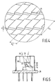
- Fig. 3 is an elevational view of an embodiment of the grating 17, viewed from the side of the radiation source 5.
- the numbers along the axes X, Y in the Figure indicate distances in micrometers.
- the horizontal lines in the Figure represent the first grating structure having a period of, for example 10 ⁇ m. Each period consists of a groove having a rectangular cross-section and a width of 5 ⁇ m and an intermediate strip having a width of 5 ⁇ m as well.
- the substantially vertical lines in the Figure represent the second grating structure whose period across the grating diameter varies from, for example 1 ⁇ m to, for example 2 ⁇ m.
- the second grating structure has, for example a sawtooth-shaped profile.
- the objective system 7 has such a position and dimensions that the radiation of the radiation source 5 falling within the circular boundary 27 of the second grating structure and being passed is also passed by the objective system and focused to the spots 8, 23, 24 on the recording layer 3.
- the horizontal lines of the first grating structure extend beyond the boundary 27. Since the monitor beam originates from the grating area within the boundary 27, the monitor beam comprises a fraction of that part of the radiation beam 6 which is used for forming the spots. Consequently, the part of the radiation beam 6 falling outside the boundary 27 is not measured. The power measured by the monitor detector 14 is thus a good measure of the power in the spots.
- Fig. 4 is an oblique elevational view of a magnification of a part of the grating 17 in which the first and second grating structures can be clearly distinguished.
- the depth of the grooves of the first grating structure is equal to that of the second grating structure.
- the period of the first grating structure is denoted by p1
- the period of the second grating structure is denoted by p2.
- the period of a grating structure determines the direction of the deflected radiation. If this grating is arranged in the device of Fig.
- the reflected part of the radiation beam 6 will be diffracted in a first order towards the monitor detector 14 due to the chosen period of the second grating structure.
- the radiation reflected by the recording layer 3 is diffracted in transmission by the second grating structure. Since, in transmission, there is a refractive index transition from the material of the plate 18 to air, the angle at which the diffracted beam exits from the grating 17 will be different than the angle at which the monitor beam 13 leaves the grating. Consequently, the radiation reflected by the record carrier does not generate any focused beams which are located very close to the monitor beam 13, which might detrimentally influence the measurement of the power in the monitor beam by the monitor detector 14.
- the detection system 12 has two detector pairs which are arranged at some distance from each other in a direction perpendicular to the plane of the drawing.
- the diffraction beams of the grating 17 will form radiation spots between said two detector pairs in the direction of the monitor detector 14. Diffraction beams, which may be present beside the monitor beam 13, will thus not influence the detection of one or more sub-beams 11 by the detection system 12.
- the depth of the grating grooves of the first grating structure in Fig. 4 is denoted by d. If this depth, measured in air, is approximately equal to half the wavelength of the radiation, combined with an approximately equal width of the grooves and the intermediate strips, only little radiation from the source 5 will be reflected by the first grating structure in diffraction beams. Since the second grating structure preferably diffracts the incident radiation in the monitor beam 13, the radiation diffracted in reflection by the grating 17 will largely be deflected in the monitor beam 13 towards the monitor detector 14.
- the angle between the long side of the sawtooth profile of the second grating structure and the plane of the grating is denoted by ⁇ in Fig. 4.
- the angle ⁇ is also referred to as blaze angle.
- the power of the monitor beam 13 diffracted in a given order may be increased at the expense of the other beams (not shown) which are diffracted in different orders by the second grating structure.
- there is a small variation of the blaze angle across the diameter of the second grating structure so as to obtain a satisfactory focusing of the monitor beam 13 on the monitor detector 14.
- the power of the side beams 21 and 22 with respect to the main beam 20 can be determined by means of the groove depth and the ratio between the width of these grooves and the intermediate strips of the first grating structure.
- the plate 18 with the gratings, the radiation source 5, the detection system 12 and the monitor detector 14 can be integrated in one radiation source-detection unit, as is shown in Fig. 5.
- the unit has a base plate 28 through which electric connections have been made.
- a cylindrical housing 29 having an aperture 30 at its upper side is mounted on the base plate.
- the inner side of the transparent plate 18 is secured to the aperture.
- the radiation source 5 in the form of a semiconductor laser is mounted on a block 31.
- the monitor detector 14 and the detection system 12 are also mounted on the block.
- a possible difference in height between the radiation source and the radiation-sensitive surface of the detectors can be compensated for by giving the second grating structure in the grating 17 and the second grating 25 a slightly different optical power.
- Some measures of a given embodiment of the radiation source-detection unit are: thickness of the plate 18:3 mm; distance between the radiation source 5 and the plate: 1.5 mm; distance between the radiation source and the centre of the monitor detector 14: 1 mm; distance between the radiation source and the centre of the detection system 12: 1.5 mm.
- the fine, blazed second grating structure is first provided in the plate 9 or 18 by means of the following steps: providing a lacquer layer on the plate, exposing the lacquer layer with a pattern in accordance with the second grating structure, developing the lacquer layer to the desired depth and converting the exposure pattern into a profile in the material of the plate by means of reactive ion etching.
- the coarser, first grating structure is provided by means of the following steps: providing a lacquer layer on the plate at the area of the second grating structure, exposing the lacquer layer with a pattern in accordance with the first grating structure, developing the lacquer layer, lowering the parts of the second grating structure corresponding to the grooves of the first grating structure to the desired depth by means of reactive ion etching, and removing the lacquer residues.
- the invention may be used advantageously in all types of devices for writing, reading and/or erasing in optical record carriers in which the information is recorded in the form of, for example pits, of areas having a different reflection coefficient than their surroundings, such as those which are formed in phase-change materials, or of magnetic domains.
- the described grating 17 having the two grating structures may be further used in all devices for scanning surfaces by means of a radiation beam. Such a surface need not be a recording surface in an optical record carrier, but it may be any arbitrary surface to be examined.
Landscapes
- Physics & Mathematics (AREA)
- Optics & Photonics (AREA)
- General Physics & Mathematics (AREA)
- Engineering & Computer Science (AREA)
- Manufacturing & Machinery (AREA)
- Optical Recording Or Reproduction (AREA)
- Optical Head (AREA)
Priority Applications (1)
| Application Number | Priority Date | Filing Date | Title |
|---|---|---|---|
| EP93203700A EP0605929B1 (de) | 1993-01-04 | 1993-12-27 | Vorrichtung zur optischen Abtastung einer Fläche |
Applications Claiming Priority (3)
| Application Number | Priority Date | Filing Date | Title |
|---|---|---|---|
| EP93200002 | 1993-01-04 | ||
| EP93200002 | 1993-01-04 | ||
| EP93203700A EP0605929B1 (de) | 1993-01-04 | 1993-12-27 | Vorrichtung zur optischen Abtastung einer Fläche |
Publications (2)
| Publication Number | Publication Date |
|---|---|
| EP0605929A1 true EP0605929A1 (de) | 1994-07-13 |
| EP0605929B1 EP0605929B1 (de) | 1998-07-29 |
Family
ID=26133584
Family Applications (1)
| Application Number | Title | Priority Date | Filing Date |
|---|---|---|---|
| EP93203700A Expired - Lifetime EP0605929B1 (de) | 1993-01-04 | 1993-12-27 | Vorrichtung zur optischen Abtastung einer Fläche |
Country Status (1)
| Country | Link |
|---|---|
| EP (1) | EP0605929B1 (de) |
Cited By (4)
| Publication number | Priority date | Publication date | Assignee | Title |
|---|---|---|---|---|
| WO1995034015A1 (en) * | 1994-06-07 | 1995-12-14 | Philips Electronics N.V. | Optical scanning device, and beam shaper and radiation source unit for use in the device |
| EP0740294A1 (de) * | 1995-04-26 | 1996-10-30 | Matsushita Electric Industrial Co., Ltd. | Optischer Kopf |
| EP0859947A4 (de) * | 1996-07-16 | 2000-04-05 | Motorola Inc | Verfahren und vorrichtung zur rückkopplung in einer optischen baugruppe |
| EP0825471B1 (de) * | 1996-08-19 | 2007-05-02 | FUJIFILM Corporation | Verfahren und Vorrichtung zum Steuern des Durchmessers eines Lichtstrahls |
Citations (11)
| Publication number | Priority date | Publication date | Assignee | Title |
|---|---|---|---|---|
| US4358200A (en) * | 1979-09-28 | 1982-11-09 | U.S. Philips Corporation | Optical focussing-error detection system |
| US4665310A (en) * | 1985-10-17 | 1987-05-12 | U.S. Philips Corporation | Apparatus for optically scanning an information plane wherein a diffraction grating splits the beam into two sub-beams |
| JPH01112534A (ja) * | 1987-10-27 | 1989-05-01 | Sharp Corp | 光ピックアップ装置 |
| JPH01241030A (ja) * | 1988-03-18 | 1989-09-26 | Sanyo Electric Co Ltd | 光出力モニタ装置 |
| EP0372629A2 (de) * | 1988-12-05 | 1990-06-13 | Koninklijke Philips Electronics N.V. | Vorrichtung zum Abtasten einer Informationsfläche mit optischer Strahlung |
| JPH02239434A (ja) * | 1989-03-10 | 1990-09-21 | Sharp Corp | 光ピックアップ |
| EP0452793A2 (de) * | 1990-04-12 | 1991-10-23 | Matsushita Electric Industrial Co., Ltd. | Optischer Kopf mit hologrammverbundener Objektivlinse |
| EP0495413A1 (de) * | 1991-01-12 | 1992-07-22 | Canon Kabushiki Kaisha | Licht-Detektionsvorrichtung mit Beugungsgitter |
| JPH04311828A (ja) * | 1991-04-10 | 1992-11-04 | Hitachi Ltd | 光ヘッドおよび情報記録装置 |
| US5212572A (en) * | 1991-11-22 | 1993-05-18 | International Business Machines Corporation | Optical data storage system with compact holographic polarization-sensing or reflectivity-sensing optical storage head |
| US5233595A (en) * | 1990-10-24 | 1993-08-03 | Olympus Optical Co., Ltd. | Optical pickup including waveguide light intensity detection means for controlling a position/intensity of a semiconductor laser |
-
1993
- 1993-12-27 EP EP93203700A patent/EP0605929B1/de not_active Expired - Lifetime
Patent Citations (11)
| Publication number | Priority date | Publication date | Assignee | Title |
|---|---|---|---|---|
| US4358200A (en) * | 1979-09-28 | 1982-11-09 | U.S. Philips Corporation | Optical focussing-error detection system |
| US4665310A (en) * | 1985-10-17 | 1987-05-12 | U.S. Philips Corporation | Apparatus for optically scanning an information plane wherein a diffraction grating splits the beam into two sub-beams |
| JPH01112534A (ja) * | 1987-10-27 | 1989-05-01 | Sharp Corp | 光ピックアップ装置 |
| JPH01241030A (ja) * | 1988-03-18 | 1989-09-26 | Sanyo Electric Co Ltd | 光出力モニタ装置 |
| EP0372629A2 (de) * | 1988-12-05 | 1990-06-13 | Koninklijke Philips Electronics N.V. | Vorrichtung zum Abtasten einer Informationsfläche mit optischer Strahlung |
| JPH02239434A (ja) * | 1989-03-10 | 1990-09-21 | Sharp Corp | 光ピックアップ |
| EP0452793A2 (de) * | 1990-04-12 | 1991-10-23 | Matsushita Electric Industrial Co., Ltd. | Optischer Kopf mit hologrammverbundener Objektivlinse |
| US5233595A (en) * | 1990-10-24 | 1993-08-03 | Olympus Optical Co., Ltd. | Optical pickup including waveguide light intensity detection means for controlling a position/intensity of a semiconductor laser |
| EP0495413A1 (de) * | 1991-01-12 | 1992-07-22 | Canon Kabushiki Kaisha | Licht-Detektionsvorrichtung mit Beugungsgitter |
| JPH04311828A (ja) * | 1991-04-10 | 1992-11-04 | Hitachi Ltd | 光ヘッドおよび情報記録装置 |
| US5212572A (en) * | 1991-11-22 | 1993-05-18 | International Business Machines Corporation | Optical data storage system with compact holographic polarization-sensing or reflectivity-sensing optical storage head |
Non-Patent Citations (4)
| Title |
|---|
| PATENT ABSTRACTS OF JAPAN vol. 13, no. 353 (P - 913) 8 August 1989 (1989-08-08) * |
| PATENT ABSTRACTS OF JAPAN vol. 13, no. 572 (P - 978) 18 December 1989 (1989-12-18) * |
| PATENT ABSTRACTS OF JAPAN vol. 14, no. 561 (P - 1142) 13 December 1990 (1990-12-13) * |
| PATENT ABSTRACTS OF JAPAN vol. 17, no. 132 (P - 1504) 18 March 1993 (1993-03-18) * |
Cited By (6)
| Publication number | Priority date | Publication date | Assignee | Title |
|---|---|---|---|---|
| WO1995034015A1 (en) * | 1994-06-07 | 1995-12-14 | Philips Electronics N.V. | Optical scanning device, and beam shaper and radiation source unit for use in the device |
| US6108138A (en) * | 1994-06-07 | 2000-08-22 | U.S. Philips Corporation | Optical beam shaper, and radiation source unit and scanning device including said beam shaper |
| EP0740294A1 (de) * | 1995-04-26 | 1996-10-30 | Matsushita Electric Industrial Co., Ltd. | Optischer Kopf |
| US5629919A (en) * | 1995-04-26 | 1997-05-13 | Matsushita Electric Industrial Co., Ltd. | Two plate-like beam splitting device |
| EP0859947A4 (de) * | 1996-07-16 | 2000-04-05 | Motorola Inc | Verfahren und vorrichtung zur rückkopplung in einer optischen baugruppe |
| EP0825471B1 (de) * | 1996-08-19 | 2007-05-02 | FUJIFILM Corporation | Verfahren und Vorrichtung zum Steuern des Durchmessers eines Lichtstrahls |
Also Published As
| Publication number | Publication date |
|---|---|
| EP0605929B1 (de) | 1998-07-29 |
Similar Documents
| Publication | Publication Date | Title |
|---|---|---|
| EP0219908B1 (de) | Gerät zur optischen Abtastung einer Informationsebene | |
| EP0305169B1 (de) | Optische Abtastvorrichtung und optische Gitteranordnung dazu | |
| US4924079A (en) | Apparatus for optically scanning an information plane | |
| EP0373700B1 (de) | Optische Abtastvorrichtung und geeignetes Spiegelobjektiv zum Anpassen an diese Vorrichtung. | |
| EP0398431B1 (de) | Retrofokus-Objektivlinse und optische Abtastanordnung mit einer derartigen Linse | |
| EP0308022B1 (de) | Vorrichtung zum Abtasten einer strahlungsreflektierenden Informationsfläche mittels optischer Strahlung | |
| EP0255173A1 (de) | Vorrichtung zur Abtastung einer strahlungzurückstrahlenden Informationsfläche mit optischer Strahlung | |
| EP0373699B1 (de) | Optische Abtastvorrichtung, geeignetes Spiegelobjektiv für diese Vorrichtung und optische Schreib- und/oder Leseanordnung mit der Abtastvorrichtung | |
| US4908506A (en) | Apparatus for optically scanning a radiation-reflecting information plane | |
| US5500846A (en) | Radiation source-detection unit employing a grating having two grating structures, and a device including that unit | |
| EP0612064B1 (de) | Optische Abtastvorrichtung | |
| EP0605929B1 (de) | Vorrichtung zur optischen Abtastung einer Fläche | |
| EP0475523B1 (de) | Vorrichtung zum Abtasten einer Informationsfläche mit optischer Strahlung | |
| US5953304A (en) | Optical disc recording or playback device with corrected focus optical scanning | |
| JP3415938B2 (ja) | 変位測定装置および光ピックアップ | |
| US20070247984A1 (en) | Optical Record Carrier and Optical Scanning Device | |
| JP2561253B2 (ja) | トラツク誤差検出装置 | |
| KR100339345B1 (ko) | 광픽업장치 |
Legal Events
| Date | Code | Title | Description |
|---|---|---|---|
| PUAI | Public reference made under article 153(3) epc to a published international application that has entered the european phase |
Free format text: ORIGINAL CODE: 0009012 |
|
| AK | Designated contracting states |
Kind code of ref document: A1 Designated state(s): AT DE FR GB |
|
| RAP1 | Party data changed (applicant data changed or rights of an application transferred) |
Owner name: N.V. PHILIPS' GLOEILAMPENFABRIEKEN |
|
| 17P | Request for examination filed |
Effective date: 19950113 |
|
| 17Q | First examination report despatched |
Effective date: 19970509 |
|
| GRAG | Despatch of communication of intention to grant |
Free format text: ORIGINAL CODE: EPIDOS AGRA |
|
| GRAG | Despatch of communication of intention to grant |
Free format text: ORIGINAL CODE: EPIDOS AGRA |
|
| GRAH | Despatch of communication of intention to grant a patent |
Free format text: ORIGINAL CODE: EPIDOS IGRA |
|
| GRAH | Despatch of communication of intention to grant a patent |
Free format text: ORIGINAL CODE: EPIDOS IGRA |
|
| GRAA | (expected) grant |
Free format text: ORIGINAL CODE: 0009210 |
|
| AK | Designated contracting states |
Kind code of ref document: B1 Designated state(s): AT DE FR GB |
|
| REF | Corresponds to: |
Ref document number: 169144 Country of ref document: AT Date of ref document: 19980815 Kind code of ref document: T |
|
| RAP4 | Party data changed (patent owner data changed or rights of a patent transferred) |
Owner name: KONINKLIJKE PHILIPS ELECTRONICS N.V. |
|
| REF | Corresponds to: |
Ref document number: 69320018 Country of ref document: DE Date of ref document: 19980903 |
|
| ET | Fr: translation filed | ||
| PLBE | No opposition filed within time limit |
Free format text: ORIGINAL CODE: 0009261 |
|
| 26N | No opposition filed | ||
| REG | Reference to a national code |
Ref country code: GB Ref legal event code: IF02 |
|
| REG | Reference to a national code |
Ref country code: GB Ref legal event code: 746 Effective date: 20040811 |
|
| REG | Reference to a national code |
Ref country code: FR Ref legal event code: D6 |
|
| PGFP | Annual fee paid to national office [announced via postgrant information from national office to epo] |
Ref country code: DE Payment date: 20060214 Year of fee payment: 13 |
|
| PGFP | Annual fee paid to national office [announced via postgrant information from national office to epo] |
Ref country code: GB Payment date: 20061218 Year of fee payment: 14 |
|
| PGFP | Annual fee paid to national office [announced via postgrant information from national office to epo] |
Ref country code: AT Payment date: 20061229 Year of fee payment: 14 |
|
| PG25 | Lapsed in a contracting state [announced via postgrant information from national office to epo] |
Ref country code: DE Free format text: LAPSE BECAUSE OF NON-PAYMENT OF DUE FEES Effective date: 20070703 |
|
| PGFP | Annual fee paid to national office [announced via postgrant information from national office to epo] |
Ref country code: FR Payment date: 20061227 Year of fee payment: 14 |
|
| GBPC | Gb: european patent ceased through non-payment of renewal fee |
Effective date: 20071227 |
|
| PG25 | Lapsed in a contracting state [announced via postgrant information from national office to epo] |
Ref country code: AT Free format text: LAPSE BECAUSE OF NON-PAYMENT OF DUE FEES Effective date: 20071227 |
|
| REG | Reference to a national code |
Ref country code: FR Ref legal event code: ST Effective date: 20081020 |
|
| PG25 | Lapsed in a contracting state [announced via postgrant information from national office to epo] |
Ref country code: GB Free format text: LAPSE BECAUSE OF NON-PAYMENT OF DUE FEES Effective date: 20071227 |
|
| PG25 | Lapsed in a contracting state [announced via postgrant information from national office to epo] |
Ref country code: FR Free format text: LAPSE BECAUSE OF NON-PAYMENT OF DUE FEES Effective date: 20071231 |