EP0605982A2 - Multi-chip module board - Google Patents
Multi-chip module board Download PDFInfo
- Publication number
- EP0605982A2 EP0605982A2 EP93310253A EP93310253A EP0605982A2 EP 0605982 A2 EP0605982 A2 EP 0605982A2 EP 93310253 A EP93310253 A EP 93310253A EP 93310253 A EP93310253 A EP 93310253A EP 0605982 A2 EP0605982 A2 EP 0605982A2
- Authority
- EP
- European Patent Office
- Prior art keywords
- chip module
- board
- module
- substrate
- modules
- Prior art date
- Legal status (The legal status is an assumption and is not a legal conclusion. Google has not performed a legal analysis and makes no representation as to the accuracy of the status listed.)
- Withdrawn
Links
Images


Classifications
-
- H—ELECTRICITY
- H05—ELECTRIC TECHNIQUES NOT OTHERWISE PROVIDED FOR
- H05K—PRINTED CIRCUITS; CASINGS OR CONSTRUCTIONAL DETAILS OF ELECTRIC APPARATUS; MANUFACTURE OF ASSEMBLAGES OF ELECTRICAL COMPONENTS
- H05K7/00—Constructional details common to different types of electric apparatus
- H05K7/02—Arrangements of circuit components or wiring on supporting structure
- H05K7/023—Stackable modules
-
- H—ELECTRICITY
- H05—ELECTRIC TECHNIQUES NOT OTHERWISE PROVIDED FOR
- H05K—PRINTED CIRCUITS; CASINGS OR CONSTRUCTIONAL DETAILS OF ELECTRIC APPARATUS; MANUFACTURE OF ASSEMBLAGES OF ELECTRICAL COMPONENTS
- H05K1/00—Printed circuits
- H05K1/02—Details
- H05K1/14—Structural association of two or more printed circuits
- H05K1/141—One or more single auxiliary printed circuits mounted on a main printed circuit, e.g. modules, adapters
-
- H—ELECTRICITY
- H05—ELECTRIC TECHNIQUES NOT OTHERWISE PROVIDED FOR
- H05K—PRINTED CIRCUITS; CASINGS OR CONSTRUCTIONAL DETAILS OF ELECTRIC APPARATUS; MANUFACTURE OF ASSEMBLAGES OF ELECTRICAL COMPONENTS
- H05K2201/00—Indexing scheme relating to printed circuits covered by H05K1/00
- H05K2201/10—Details of components or other objects attached to or integrated in a printed circuit board
- H05K2201/10007—Types of components
- H05K2201/10159—Memory
-
- H—ELECTRICITY
- H05—ELECTRIC TECHNIQUES NOT OTHERWISE PROVIDED FOR
- H05K—PRINTED CIRCUITS; CASINGS OR CONSTRUCTIONAL DETAILS OF ELECTRIC APPARATUS; MANUFACTURE OF ASSEMBLAGES OF ELECTRICAL COMPONENTS
- H05K2201/00—Indexing scheme relating to printed circuits covered by H05K1/00
- H05K2201/10—Details of components or other objects attached to or integrated in a printed circuit board
- H05K2201/10613—Details of electrical connections of non-printed components, e.g. special leads
- H05K2201/10621—Components characterised by their electrical contacts
- H05K2201/10689—Leaded Integrated Circuit [IC] package, e.g. dual-in-line [DIL]
-
- H—ELECTRICITY
- H05—ELECTRIC TECHNIQUES NOT OTHERWISE PROVIDED FOR
- H05K—PRINTED CIRCUITS; CASINGS OR CONSTRUCTIONAL DETAILS OF ELECTRIC APPARATUS; MANUFACTURE OF ASSEMBLAGES OF ELECTRICAL COMPONENTS
- H05K2203/00—Indexing scheme relating to apparatus or processes for manufacturing printed circuits covered by H05K3/00
- H05K2203/15—Position of the PCB during processing
- H05K2203/1572—Processing both sides of a PCB by the same process; Providing a similar arrangement of components on both sides; Making interlayer connections from two sides
-
- H—ELECTRICITY
- H05—ELECTRIC TECHNIQUES NOT OTHERWISE PROVIDED FOR
- H05K—PRINTED CIRCUITS; CASINGS OR CONSTRUCTIONAL DETAILS OF ELECTRIC APPARATUS; MANUFACTURE OF ASSEMBLAGES OF ELECTRICAL COMPONENTS
- H05K3/00—Apparatus or processes for manufacturing printed circuits
- H05K3/36—Assembling printed circuits with other printed circuits
- H05K3/366—Assembling printed circuits with other printed circuits substantially perpendicularly to each other
Definitions
- the present invention relates generally to the interconnection of integrated circuits, and more particularly, to a multi-chip module board capable of supporting multiple multi-chip modules, memory modules and other add-on components on a single high density substrate.
- a multi-chip module (MCM) board is defined as any advanced semiconductor substrate which provides an interconnect path between electrical components mounted thereon without the need for placement of the components in predetermined positions.
- the electrical components are often integrated circuits, but may also comprise discrete circuit components such as resistors, capacitors, inductors, transistors and diodes.
- a multi-chip module board comprising: a multi-chip module substrate; and a first multi-chip module secured to said substrate; characterized by a space on said substrate configured to receive a second multi-chip module and to connect said second multi-chip module to said first multi-chip module.
- the multi-chip module board is rectangular shaped.
- the first multi-chip module containing integrated and discrete circuit elements necessary to provide the basic functions required by the board user, is mounted in the center of the module board.
- Space and connecting structure is provided on two sides of the main module for the connection of add-on modules which provide additional or peripheral functions to the board.
- the connecting structures included on the module board and the add-on modules are designed to permit the attachment of any one of several different function add-on modules to a location on the module board.
- the present invention provides a multi-chip module board having mounted thereto a main multi-chip module enabling standard functions and additional area and structure on the board for the connection of additional multi-chip modules, memory modules or component modules providing specific optional functions. Two possible embodiments of the present invention will now be described with reference to Figures 1, 2 and 3.
- FIG 1 is a perspective view of a rectangular multi-chip module (MCM) board 12 and a main multi-chip module 15 built into or mounted on the board. Space is provided on the board 12 left and right of main module 15 for the connection of additional modules 21 to 27.
- MCM multi-chip module
- MCM board 12 is a high density substrate manufactured utilizing standard MCM technology, such as cofired aluminum with CU/PI, AIN with CU/PI, or AIN only.
- PGA, edge or bottom connectors are provided for connecting the module board to other computer system components.
- An edge connector 48 is illustrated in Figure 1.
- Main module 15 contains integrated and discrete components necessary to provide the basic functions required by the board user.
- the components are housed under a protective lid.
- the add-on modules 21 through 27 are attached to the board to provide additional or peripheral functions.
- the additional modules could include, for example, a Small Computer System Interface (SCSI) chip, a math coprocessor, memory, a testing cache or other integrated or discrete components.
- Connecting structure is included on board 12 for mating with the add-on modules. This connecting structure could comprise solder balls, SMT, PGA sockets, bump connection, or any other known connecting means.
- the connecting structure for module 21 shown in Figure 1 comprises pin connectors 52 positioned on the bottom of add-on module 21 and corresponding pin holes 54 in the MCM board substrate.
- the connecting structures included on board 12 and the add-on modules are preferably designed such that a common connecting interface is provided. This common interface would permit the attachment of any one of several different function add-on modules to a location on board 12.
- the board design shown in Figure 1 provides connection for add-on modules on two sides (left and right) of main module 15.
- the board design can easily be expanded to provide an MCM module attachment area on all four sides of main the MCM module 15.
- Figures 2 and 3 show another embodiment of the present invention wherein the main MCM module 15 occupies all of one side of the MCM board 12.
- Figure 2 shows a plurality of add-on MCM modules 31 to 46 optionally connected to the top side of board 12.
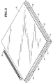
- Main module 15 is connected to the bottom side of board 12 as shown in Figure 3.
- An edge connector 48 provides for connection of the module board to other computer system components.
- the module board as described above provides a multi-chip module board "motherboard” which includes a main MCM module providing standard functions and provisions for the attachment of additional MCM modules, memory modules or other components empowering the MCM board with specific, optional, high performance functionality.
- the MCM board includes a first area permanently occupied by the main MCM module with the remainder of the MCM board providing contact area for the connection of additional, optional MCM modules, single chip packages, or other discrete components.
- the main MCM module may occupy one side of the MCM motherboard while the other side of the MCM board provides contact area for the additional MCM modules or single chip packages.
- the primary advantage provided by the MCM board structure described above is the capability of operating computer peripherals and options at greater speeds, e.g., processor speed, thereby improving overall system performance.
- the shape of the board and layout of modules, components and connecting structure can be varied from that shown in Figures 1 and 2.
Landscapes
- Engineering & Computer Science (AREA)
- Microelectronics & Electronic Packaging (AREA)
- Combinations Of Printed Boards (AREA)
Abstract
Description
- The present invention relates generally to the interconnection of integrated circuits, and more particularly, to a multi-chip module board capable of supporting multiple multi-chip modules, memory modules and other add-on components on a single high density substrate.
- A multi-chip module (MCM) board is defined as any advanced semiconductor substrate which provides an interconnect path between electrical components mounted thereon without the need for placement of the components in predetermined positions. The electrical components are often integrated circuits, but may also comprise discrete circuit components such as resistors, capacitors, inductors, transistors and diodes.
- With the arrival of higher speed computer processors, e.g. 66 megahertz and greater, the need to accelerate other computer functions has become evident. The slower speed of the memory bus and other peripherals, such as a coprocessor, limit the overall performance of the computer system and restrict the benefits to be gained from the higher speed processor. The incorporation of peripheral functions onto multi-chip modules provides a method for increasing the speed of those operations.
- As the inclusion and arrangement of components on a multi-chip module will vary according to each application, the process to prepare a multi-chip module for each application must also be varied. Those skilled in the art will recognize that there are numerous benefits to be gained from standardizing the process of manufacturing multi-chip modules.
- It is an object of the present invention to provide a multi-chip module board which can be customized through the attachment of additional multi-chip modules, memory modules or other components.
- According to the present invention there is provided a multi-chip module board, comprising: a multi-chip module substrate; and a first multi-chip module secured to said substrate; characterized by a space on said substrate configured to receive a second multi-chip module and to connect said second multi-chip module to said first multi-chip module.
- In the described embodiment, the multi-chip module board is rectangular shaped. The first multi-chip module, containing integrated and discrete circuit elements necessary to provide the basic functions required by the board user, is mounted in the center of the module board. Space and connecting structure is provided on two sides of the main module for the connection of add-on modules which provide additional or peripheral functions to the board. The connecting structures included on the module board and the add-on modules are designed to permit the attachment of any one of several different function add-on modules to a location on the module board.
- Embodiments of the present invention will now be described, by way of example. with reference to the accompanying drawings, in which:
- Figure 1 is a perspective view of a multi-chip module built into or mounted on a rectangular module board including additional area adjacent the multi-chip module for the connection of additional multi-chip modules, memory module or other components in accordance with the present invention;
- Figure 2 provides a perspective view of another multi-chip module mounted on one side of a rectangular module board including additional area on the second side of the module board for the connection of additional multi-chip modules, memory modules or other components in accordance with the present invention; and
- Figure 3 provides a view of the underside of the multi-chip module board shown in Figure 2.
- Those skilled in the art will recognize that the components and circuitry on a multi-chip module will vary according to each application. With the foregoing in mind, the present invention provides a multi-chip module board having mounted thereto a main multi-chip module enabling standard functions and additional area and structure on the board for the connection of additional multi-chip modules, memory modules or component modules providing specific optional functions. Two possible embodiments of the present invention will now be described with reference to Figures 1, 2 and 3.
- Figure 1 is a perspective view of a rectangular multi-chip module (MCM)
board 12 and a mainmulti-chip module 15 built into or mounted on the board. Space is provided on theboard 12 left and right ofmain module 15 for the connection ofadditional modules 21 to 27. -
MCM board 12 is a high density substrate manufactured utilizing standard MCM technology, such as cofired aluminum with CU/PI, AIN with CU/PI, or AIN only. PGA, edge or bottom connectors are provided for connecting the module board to other computer system components. Anedge connector 48 is illustrated in Figure 1. -
Main module 15 contains integrated and discrete components necessary to provide the basic functions required by the board user. The components are housed under a protective lid. The add-onmodules 21 through 27 are attached to the board to provide additional or peripheral functions. The additional modules could include, for example, a Small Computer System Interface (SCSI) chip, a math coprocessor, memory, a testing cache or other integrated or discrete components. Connecting structure is included onboard 12 for mating with the add-on modules. This connecting structure could comprise solder balls, SMT, PGA sockets, bump connection, or any other known connecting means. The connecting structure formodule 21 shown in Figure 1 comprisespin connectors 52 positioned on the bottom of add-onmodule 21 andcorresponding pin holes 54 in the MCM board substrate. - The connecting structures included on
board 12 and the add-on modules are preferably designed such that a common connecting interface is provided. This common interface would permit the attachment of any one of several different function add-on modules to a location onboard 12. - The board design shown in Figure 1 provides connection for add-on modules on two sides (left and right) of
main module 15. The board design can easily be expanded to provide an MCM module attachment area on all four sides of main theMCM module 15. - Figures 2 and 3 show another embodiment of the present invention wherein the
main MCM module 15 occupies all of one side of theMCM board 12. Figure 2 shows a plurality of add-onMCM modules 31 to 46 optionally connected to the top side ofboard 12.Main module 15 is connected to the bottom side ofboard 12 as shown in Figure 3. Anedge connector 48 provides for connection of the module board to other computer system components. - The board, connecting structures, and add-on modules are manufactured as set forth above in the description of the embodiment of the invention shown in Figure 1.
- The module board as described above provides a multi-chip module board "motherboard" which includes a main MCM module providing standard functions and provisions for the attachment of additional MCM modules, memory modules or other components empowering the MCM board with specific, optional, high performance functionality. The MCM board includes a first area permanently occupied by the main MCM module with the remainder of the MCM board providing contact area for the connection of additional, optional MCM modules, single chip packages, or other discrete components. Alternatively, the main MCM module may occupy one side of the MCM motherboard while the other side of the MCM board provides contact area for the additional MCM modules or single chip packages.
- The primary advantage provided by the MCM board structure described above is the capability of operating computer peripherals and options at greater speeds, e.g., processor speed, thereby improving overall system performance.
- In view of the foregoing it will be clear to a person skilled in the art that modifications may be incorporated without departing from the scope of the present invention.
- For example, the shape of the board and layout of modules, components and connecting structure can be varied from that shown in Figures 1 and 2.
Claims (8)
- A multi-chip module board, comprising: a multi-chip module substrate; and a first multi-chip module secured to said substrate; characterized by a space on said substrate configured to receive a second multi-chip module and to connect said second multi-chip module to said first multi-chip module.
- A multi-chip module board as claimed in claim 1, characterized in that said substrate has a first side and a second side, and said first multi-chip module is secured to said first side, and said space is located on said first side.
- A multi-chip module board as claimed in claim 2, further comprising another space, on said second side of said substrate, configured to receive a third multi-chip module and to operatively connect said third multi-chip module to said first multi-chip module.
- A multi-chip module board as claimed in claim 1, wherein said substrate has a first side and a second side, and said first multi-chip module is secured to said first side and said space is located on said second side.
- A multi-chip module board as claimed in claim 3 or claim 4, further comprising an edge connector operatively connected to said first multi-chip module and extending to a peripheral portion of said substrate.
- A multi-chip module board according to any previous claim, further comprising a second multi-chip module secured to said space on said substrate and operatively connected to said first multi-chip module.
- A multi-chip module board as claimed in claim 1, further comprising a customizing means, operatively connected to said substrate, for customizing the board to facilitate a particular application, and including a connecting means for operatively connecting a customized set of additional multi-chip modules to said main multi-chip module, wherein said customized set is selected from a group of customized sets, each of which is designed to facilitate a particular application, and said customizing means is configured to accommodate any one of said customized sets.
- A multi-chip module board as claimed in claim 7, characterized in that said space is configured to accommodate more than one type of multi-chip module.
Applications Claiming Priority (2)
| Application Number | Priority Date | Filing Date | Title |
|---|---|---|---|
| US996993 | 1992-12-28 | ||
| US07/996,993 US5303121A (en) | 1992-12-28 | 1992-12-28 | Multi-chip module board |
Publications (2)
| Publication Number | Publication Date |
|---|---|
| EP0605982A2 true EP0605982A2 (en) | 1994-07-13 |
| EP0605982A3 EP0605982A3 (en) | 1994-07-27 |
Family
ID=25543527
Family Applications (1)
| Application Number | Title | Priority Date | Filing Date |
|---|---|---|---|
| EP19930310253 Withdrawn EP0605982A3 (en) | 1992-12-28 | 1993-12-17 | Multi-chip module board. |
Country Status (3)
| Country | Link |
|---|---|
| US (1) | US5303121A (en) |
| EP (1) | EP0605982A3 (en) |
| JP (1) | JPH077135A (en) |
Cited By (1)
| Publication number | Priority date | Publication date | Assignee | Title |
|---|---|---|---|---|
| CN106375496A (en) * | 2015-07-24 | 2017-02-01 | 富士康(昆山)电脑接插件有限公司 | Electronic device |
Families Citing this family (37)
| Publication number | Priority date | Publication date | Assignee | Title |
|---|---|---|---|---|
| US5369552A (en) * | 1992-07-14 | 1994-11-29 | Ncr Corporation | Multi-chip module with multiple compartments |
| US5649224A (en) * | 1993-01-26 | 1997-07-15 | Intel Corporation | Integrated circuit card having contacts along the side rails and method for transferring information using the contacts |
| US5501608A (en) * | 1993-12-20 | 1996-03-26 | Intel Corporation | Computer system with an interconnection receptacle suitable for different external connectors |
| US5619660A (en) * | 1994-04-28 | 1997-04-08 | Intel Corporation | Keying notches for side contacts on a thin form factor computer card |
| US5525795A (en) * | 1994-05-24 | 1996-06-11 | Intel Corporation | Voltage protection for add in cards with sideswipe contacts |
| US5526217A (en) * | 1994-05-24 | 1996-06-11 | Intel Corporation | Voltage protection for modem add in cards with sideswipe contacts |
| US5889866A (en) * | 1994-06-30 | 1999-03-30 | Intel Corporation | Method and apparatus for controlling access to detachably connectable computer devices using an encrypted password |
| US5477418A (en) * | 1994-07-15 | 1995-12-19 | Intel Corporation | I/O connector for add in printed circuit cards for computer systems |
| US5563769A (en) * | 1994-07-19 | 1996-10-08 | Intel Corporation | Tabbed cover attach for PCMCIA card packaging and method for attaching the PCMCIA covers to the printed circuit board assembly |
| US5475592A (en) * | 1994-10-21 | 1995-12-12 | United Technologies Automotive, Inc. | Optical plug-in memory pack for positioning control |
| US5606704A (en) * | 1994-10-26 | 1997-02-25 | Intel Corporation | Active power down for PC card I/O applications |
| US5637018A (en) * | 1994-11-01 | 1997-06-10 | Intel Corporation | Hi-jack hinged connection adapter for input/output cards |
| USD369588S (en) | 1994-11-04 | 1996-05-07 | Metropage, Inc. | Heat seal connector for a pager |
| US5870290A (en) * | 1994-11-30 | 1999-02-09 | Intel Corporation | Interface adapter board having arrays of interstitial connectors and an intermediate switching circuit |
| USD370464S (en) | 1994-11-30 | 1996-06-04 | Metropage, Inc. | Heat seal connector for a pager |
| US6188874B1 (en) | 1997-06-27 | 2001-02-13 | Lockheed Martin Corporation | Control and telemetry signal communication system for geostationary satellites |
| US6507210B1 (en) * | 2000-11-22 | 2003-01-14 | Ulysses Esd, Inc. | System and method for power testing a chassis |
| RU2183884C1 (en) * | 2000-12-21 | 2002-06-20 | СИНЕРДЖЕСТИК КОМПЬЮТИНГ СИСТЕМС (СИКС) АпС | Multilayer hybrid electronic module |
| JP2002246704A (en) * | 2001-02-16 | 2002-08-30 | Philips Japan Ltd | Electronic device and circuit device |
| US6626681B2 (en) * | 2002-02-21 | 2003-09-30 | Intel Corporation | Integrated socket for microprocessor package and cache memory |
| US7326857B2 (en) * | 2004-11-18 | 2008-02-05 | International Business Machines Corporation | Method and structure for creating printed circuit boards with stepped thickness |
| US7212408B2 (en) * | 2004-12-28 | 2007-05-01 | Intel Corporation | Multi-slot socket for mounting integrated circuits on circuit board |
| TWM281269U (en) * | 2005-06-24 | 2005-11-21 | Optimum Care Int Tech Inc | Conducting apparatus for memory component |
| US20070064401A1 (en) * | 2005-09-16 | 2007-03-22 | Lih Duo International Co., Ltd. | Printed circuit board and memory module using the same |
| TW200905440A (en) * | 2007-07-25 | 2009-02-01 | Asustek Comp Inc | Modular motherboard |
| US20100053925A1 (en) * | 2008-09-03 | 2010-03-04 | Chao-Tsung Huang | Chip mount for data storage device |
| JP1528936S (en) * | 2015-01-14 | 2015-07-13 | ||
| JP1528484S (en) * | 2015-01-14 | 2015-07-13 | ||
| JP1528485S (en) * | 2015-01-14 | 2015-07-13 | ||
| TWI598721B (en) * | 2015-07-13 | 2017-09-11 | 鴻騰精密科技股份有限公司 | Electrical device |
| US20170322601A1 (en) * | 2016-05-04 | 2017-11-09 | R-Stor Inc. | Apparatus for configuring a memory drive device |
| US10334334B2 (en) * | 2016-07-22 | 2019-06-25 | Intel Corporation | Storage sled and techniques for a data center |
| TWD190983S (en) * | 2017-02-17 | 2018-06-11 | 三星電子股份有限公司 | Ssd storage device |
| CN109388195A (en) * | 2017-08-03 | 2019-02-26 | 华硕电脑股份有限公司 | Computer system and mainboard thereof |
| USD869469S1 (en) * | 2018-04-09 | 2019-12-10 | Samsung Electronics Co., Ltd. | SSD storage device |
| AU201815958S (en) * | 2018-04-09 | 2018-11-06 | Samsung Electronics Co Ltd | SSD Storage Device |
| US10667398B1 (en) * | 2018-09-26 | 2020-05-26 | United States Of America As Represented By The Administrator Of Nasa | Dual dynamic random (DDR) access memory interface design for aerospace printed circuit boards |
Family Cites Families (8)
| Publication number | Priority date | Publication date | Assignee | Title |
|---|---|---|---|---|
| GB2053566B (en) * | 1979-07-02 | 1984-05-02 | Mostek Corp | Integrated circuit package |
| JPS5687395A (en) * | 1979-12-18 | 1981-07-15 | Fujitsu Ltd | Semiconductor device |
| JPS58159360A (en) * | 1982-03-17 | 1983-09-21 | Fujitsu Ltd | Semiconductor device |
| US4600968A (en) * | 1984-11-13 | 1986-07-15 | Fuji Electric Co., Ltd. | Semiconductor device package having regions of different thermal properties |
| US4706166A (en) * | 1986-04-25 | 1987-11-10 | Irvine Sensors Corporation | High-density electronic modules--process and product |
| US4983533A (en) * | 1987-10-28 | 1991-01-08 | Irvine Sensors Corporation | High-density electronic modules - process and product |
| US4891789A (en) * | 1988-03-03 | 1990-01-02 | Bull Hn Information Systems, Inc. | Surface mounted multilayer memory printed circuit board |
| US4998180A (en) * | 1989-05-23 | 1991-03-05 | Clearpoint Research Corporation | Bus device with closely spaced double sided daughter board |
-
1992
- 1992-12-28 US US07/996,993 patent/US5303121A/en not_active Expired - Lifetime
-
1993
- 1993-12-17 EP EP19930310253 patent/EP0605982A3/en not_active Withdrawn
- 1993-12-27 JP JP5347266A patent/JPH077135A/en active Pending
Cited By (1)
| Publication number | Priority date | Publication date | Assignee | Title |
|---|---|---|---|---|
| CN106375496A (en) * | 2015-07-24 | 2017-02-01 | 富士康(昆山)电脑接插件有限公司 | Electronic device |
Also Published As
| Publication number | Publication date |
|---|---|
| EP0605982A3 (en) | 1994-07-27 |
| US5303121A (en) | 1994-04-12 |
| JPH077135A (en) | 1995-01-10 |
Similar Documents
| Publication | Publication Date | Title |
|---|---|---|
| EP0605982A2 (en) | Multi-chip module board | |
| US5266833A (en) | Integrated circuit bus structure | |
| US5982633A (en) | Opposed ball grid array mounting | |
| US6900529B2 (en) | Electronic module having a three dimensional array of carrier-mounted integrated circuit packages | |
| US6713854B1 (en) | Electronic circuit module with a carrier having a mounting pad array | |
| EP1327265B1 (en) | Electronic module having canopy-type carriers | |
| US5198965A (en) | Free form packaging of specific functions within a computer system | |
| US5229917A (en) | VLSI integration into a 3-D WSI dual composite module | |
| US5426263A (en) | Electronic assembly having a double-sided leadless component | |
| US6160718A (en) | Multi-chip package with stacked chips and interconnect bumps | |
| EP0535479A1 (en) | Multichip integrated circuit packages and systems | |
| EP0324244A2 (en) | Tape automated bonding package for a semiconductor chip with decoupling | |
| US5789816A (en) | Multiple-chip integrated circuit package including a dummy chip | |
| US6011695A (en) | External bus interface printed circuit board routing for a ball grid array integrated circuit package | |
| US5734559A (en) | Staggered bond finger design for fine pitch integrated circuit packages | |
| US5892275A (en) | High performance power and ground edge connect IC package | |
| US5319243A (en) | Electronic assembly with first and second substrates | |
| US5801450A (en) | Variable pitch stagger die for optimal density | |
| US5870290A (en) | Interface adapter board having arrays of interstitial connectors and an intermediate switching circuit | |
| JPH03121501A (en) | Controller | |
| WO2000004595A2 (en) | Land-side mounting of components to an integrated circuit package | |
| US6256189B1 (en) | Heat slug design which facilitates mounting of discrete components on a package without losing lands or pins in the package | |
| JPH11260959A (en) | Semiconductor package | |
| JPH05190765A (en) | Semiconductor device | |
| HK1057645B (en) | Electronic module having canopy-type carriers |
Legal Events
| Date | Code | Title | Description |
|---|---|---|---|
| PUAI | Public reference made under article 153(3) epc to a published international application that has entered the european phase |
Free format text: ORIGINAL CODE: 0009012 |
|
| PUAL | Search report despatched |
Free format text: ORIGINAL CODE: 0009013 |
|
| AK | Designated contracting states |
Kind code of ref document: A2 Designated state(s): DE FR GB |
|
| AK | Designated contracting states |
Kind code of ref document: A3 Designated state(s): DE FR GB |
|
| RAP1 | Party data changed (applicant data changed or rights of an application transferred) |
Owner name: AT&T GLOBAL INFORMATION SOLUTIONS INTERNATIONAL IN |
|
| 17P | Request for examination filed |
Effective date: 19950123 |
|
| RAP1 | Party data changed (applicant data changed or rights of an application transferred) |
Owner name: HYUNDAI ELECTRONICS AMERICA Owner name: AT&T GLOBAL INFORMATION SOLUTIONS INTERNATIONAL IN |
|
| RAP1 | Party data changed (applicant data changed or rights of an application transferred) |
Owner name: SYMBIOS LOGIC INC. Owner name: HYUNDAI ELECTRONICS AMERICA Owner name: AT&T GLOBAL INFORMATION SOLUTIONS INTERNATIONAL IN |
|
| 17Q | First examination report despatched |
Effective date: 19960927 |
|
| RAP1 | Party data changed (applicant data changed or rights of an application transferred) |
Owner name: SYMBIOS LOGIC INC. Owner name: HYUNDAI ELECTRONICS AMERICA Owner name: NCR INTERNATIONAL, INC. |
|
| RAP1 | Party data changed (applicant data changed or rights of an application transferred) |
Owner name: SYMBIOS, INC. Owner name: HYUNDAI ELECTRONICS AMERICA Owner name: NCR INTERNATIONAL, INC. |
|
| STAA | Information on the status of an ep patent application or granted ep patent |
Free format text: STATUS: THE APPLICATION HAS BEEN WITHDRAWN |
|
| 18W | Application withdrawn |
Withdrawal date: 19991002 |