EP0606745A1 - Beschichtungsapparatur mit Kollimator - Google Patents
Beschichtungsapparatur mit Kollimator Download PDFInfo
- Publication number
- EP0606745A1 EP0606745A1 EP93310163A EP93310163A EP0606745A1 EP 0606745 A1 EP0606745 A1 EP 0606745A1 EP 93310163 A EP93310163 A EP 93310163A EP 93310163 A EP93310163 A EP 93310163A EP 0606745 A1 EP0606745 A1 EP 0606745A1
- Authority
- EP
- European Patent Office
- Prior art keywords
- workpiece
- sputtering
- film
- collimator
- titanium
- Prior art date
- Legal status (The legal status is an assumption and is not a legal conclusion. Google has not performed a legal analysis and makes no representation as to the accuracy of the status listed.)
- Granted
Links
Images



Classifications
-
- H—ELECTRICITY
- H01—ELECTRIC ELEMENTS
- H01J—ELECTRIC DISCHARGE TUBES OR DISCHARGE LAMPS
- H01J37/00—Discharge tubes with provision for introducing objects or material to be exposed to the discharge, e.g. for the purpose of examination or processing thereof
- H01J37/32—Gas-filled discharge tubes
- H01J37/34—Gas-filled discharge tubes operating with cathodic sputtering
- H01J37/3411—Constructional aspects of the reactor
- H01J37/3447—Collimators, shutters, apertures
-
- H—ELECTRICITY
- H01—ELECTRIC ELEMENTS
- H01J—ELECTRIC DISCHARGE TUBES OR DISCHARGE LAMPS
- H01J37/00—Discharge tubes with provision for introducing objects or material to be exposed to the discharge, e.g. for the purpose of examination or processing thereof
- H01J37/32—Gas-filled discharge tubes
- H01J37/34—Gas-filled discharge tubes operating with cathodic sputtering
- H01J37/3476—Testing and control
-
- C—CHEMISTRY; METALLURGY
- C23—COATING METALLIC MATERIAL; COATING MATERIAL WITH METALLIC MATERIAL; CHEMICAL SURFACE TREATMENT; DIFFUSION TREATMENT OF METALLIC MATERIAL; COATING BY VACUUM EVAPORATION, BY SPUTTERING, BY ION IMPLANTATION OR BY CHEMICAL VAPOUR DEPOSITION, IN GENERAL; INHIBITING CORROSION OF METALLIC MATERIAL OR INCRUSTATION IN GENERAL
- C23C—COATING METALLIC MATERIAL; COATING MATERIAL WITH METALLIC MATERIAL; SURFACE TREATMENT OF METALLIC MATERIAL BY DIFFUSION INTO THE SURFACE, BY CHEMICAL CONVERSION OR SUBSTITUTION; COATING BY VACUUM EVAPORATION, BY SPUTTERING, BY ION IMPLANTATION OR BY CHEMICAL VAPOUR DEPOSITION, IN GENERAL
- C23C14/00—Coating by vacuum evaporation, by sputtering or by ion implantation of the coating forming material
- C23C14/04—Coating on selected surface areas, e.g. using masks
- C23C14/046—Coating cavities or hollow spaces, e.g. interior of tubes; Infiltration of porous substrates
-
- C—CHEMISTRY; METALLURGY
- C23—COATING METALLIC MATERIAL; COATING MATERIAL WITH METALLIC MATERIAL; CHEMICAL SURFACE TREATMENT; DIFFUSION TREATMENT OF METALLIC MATERIAL; COATING BY VACUUM EVAPORATION, BY SPUTTERING, BY ION IMPLANTATION OR BY CHEMICAL VAPOUR DEPOSITION, IN GENERAL; INHIBITING CORROSION OF METALLIC MATERIAL OR INCRUSTATION IN GENERAL
- C23C—COATING METALLIC MATERIAL; COATING MATERIAL WITH METALLIC MATERIAL; SURFACE TREATMENT OF METALLIC MATERIAL BY DIFFUSION INTO THE SURFACE, BY CHEMICAL CONVERSION OR SUBSTITUTION; COATING BY VACUUM EVAPORATION, BY SPUTTERING, BY ION IMPLANTATION OR BY CHEMICAL VAPOUR DEPOSITION, IN GENERAL
- C23C14/00—Coating by vacuum evaporation, by sputtering or by ion implantation of the coating forming material
- C23C14/22—Coating by vacuum evaporation, by sputtering or by ion implantation of the coating forming material characterised by the process of coating
- C23C14/34—Sputtering
-
- C—CHEMISTRY; METALLURGY
- C23—COATING METALLIC MATERIAL; COATING MATERIAL WITH METALLIC MATERIAL; CHEMICAL SURFACE TREATMENT; DIFFUSION TREATMENT OF METALLIC MATERIAL; COATING BY VACUUM EVAPORATION, BY SPUTTERING, BY ION IMPLANTATION OR BY CHEMICAL VAPOUR DEPOSITION, IN GENERAL; INHIBITING CORROSION OF METALLIC MATERIAL OR INCRUSTATION IN GENERAL
- C23C—COATING METALLIC MATERIAL; COATING MATERIAL WITH METALLIC MATERIAL; SURFACE TREATMENT OF METALLIC MATERIAL BY DIFFUSION INTO THE SURFACE, BY CHEMICAL CONVERSION OR SUBSTITUTION; COATING BY VACUUM EVAPORATION, BY SPUTTERING, BY ION IMPLANTATION OR BY CHEMICAL VAPOUR DEPOSITION, IN GENERAL
- C23C14/00—Coating by vacuum evaporation, by sputtering or by ion implantation of the coating forming material
- C23C14/22—Coating by vacuum evaporation, by sputtering or by ion implantation of the coating forming material characterised by the process of coating
- C23C14/34—Sputtering
- C23C14/35—Sputtering by application of a magnetic field, e.g. magnetron sputtering
-
- C—CHEMISTRY; METALLURGY
- C23—COATING METALLIC MATERIAL; COATING MATERIAL WITH METALLIC MATERIAL; CHEMICAL SURFACE TREATMENT; DIFFUSION TREATMENT OF METALLIC MATERIAL; COATING BY VACUUM EVAPORATION, BY SPUTTERING, BY ION IMPLANTATION OR BY CHEMICAL VAPOUR DEPOSITION, IN GENERAL; INHIBITING CORROSION OF METALLIC MATERIAL OR INCRUSTATION IN GENERAL
- C23C—COATING METALLIC MATERIAL; COATING MATERIAL WITH METALLIC MATERIAL; SURFACE TREATMENT OF METALLIC MATERIAL BY DIFFUSION INTO THE SURFACE, BY CHEMICAL CONVERSION OR SUBSTITUTION; COATING BY VACUUM EVAPORATION, BY SPUTTERING, BY ION IMPLANTATION OR BY CHEMICAL VAPOUR DEPOSITION, IN GENERAL
- C23C14/00—Coating by vacuum evaporation, by sputtering or by ion implantation of the coating forming material
- C23C14/22—Coating by vacuum evaporation, by sputtering or by ion implantation of the coating forming material characterised by the process of coating
- C23C14/54—Controlling or regulating the coating process
- C23C14/548—Controlling the composition
-
- H—ELECTRICITY
- H01—ELECTRIC ELEMENTS
- H01J—ELECTRIC DISCHARGE TUBES OR DISCHARGE LAMPS
- H01J37/00—Discharge tubes with provision for introducing objects or material to be exposed to the discharge, e.g. for the purpose of examination or processing thereof
- H01J37/32—Gas-filled discharge tubes
- H01J37/34—Gas-filled discharge tubes operating with cathodic sputtering
- H01J37/3402—Gas-filled discharge tubes operating with cathodic sputtering using supplementary magnetic fields
- H01J37/3405—Magnetron sputtering
- H01J37/3408—Planar magnetron sputtering
-
- H—ELECTRICITY
- H01—ELECTRIC ELEMENTS
- H01J—ELECTRIC DISCHARGE TUBES OR DISCHARGE LAMPS
- H01J37/00—Discharge tubes with provision for introducing objects or material to be exposed to the discharge, e.g. for the purpose of examination or processing thereof
- H01J37/32—Gas-filled discharge tubes
- H01J37/34—Gas-filled discharge tubes operating with cathodic sputtering
- H01J37/3488—Constructional details of particle beam apparatus not otherwise provided for, e.g. arrangement, mounting, housing, environment; special provisions for cleaning or maintenance of the apparatus
- H01J37/3494—Adaptation to extreme pressure conditions
Definitions
- This invention pertains generally to sputter coating and, more particularly, to an apparatus and a method for depositing a thin film coating and, more particularly, to an apparatus and a method for depositing a thin film coating on a workpiece by collimated sputtering.
- Sputter coating is commonly employed in the formation of films on substrates in the manufacture of semiconductor devices. Planar magnetrons have long been used as sputtering devices to coat silicon wafers with various materials during the manufacture of integrated circuits. While aluminium has traditionally been the most common metallization material used in integrated circuits, other sputtered materials, such as titanium, titanium nitride, and titanium/tungsten alloy are now also commonly being used. Sputtering is also used during semiconductor manufacturing to deposit various non-metallic compounds either by direct sputtering or by reactive sputtering. Some of these non-metallic compounds, such as titanium nitride, are sufficiently conductive to be used in interconnect structures.
- Particles (atoms) which arrive at angles much different than normal to the substrate surface tend to produce lateral growth on the surface. This lateral growth can result in overgrowth at the tops of the openings which can eventually close off via openings before they can be properly coated, resulting, for example, in an adequate electrical connection between integrated circuit layers.
- the collimating filter typically comprises a plurality of cells in an array which is interposed between a sputter source and a workpiece.
- atoms emitted from the sputter source must pass through the cells without striking the cell walls, i.e., the cell walls intercept sputtered particles travelling at angles which are not close to being normal to the substrate. This causes a substantial amount of sputtered material to deposit on the filter itself.
- the inventors of this invention have determined that the problem of extraneous particle creation is, in part, related to the mismatch in the thermal coefficients of expansion (TCE's) between the material used to construct the collimation filter and the material being sputtered.
- TCE's thermal coefficients of expansion
- the filter, and the film deposited on it, go through substantial thermal cycling as the sputtering equipment is used.
- a collimating filter may initially be at room temperature when the system is started, and then be heated to several hundred degrees centigrade as the system is operated.
- the inventors have also recognized that the degree to which thermal mismatch causes problems is dependent on the properties of the material being deposited and the material used to construct the filter.
- the problem is particularly acute when depositing non-metallic materials which tend to have low ductility and are more prone to flaking.
- Most metallic films have sufficiently high ductility and adhesion so that they can tolerate appreciable mismatch in TCE between the film and the collimator.
- many non-metallic materials that are commonly deposited by sputtering, such as titanium nitride are brittle and prone to flaking.
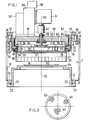
- the sputtering apparatus has a housing 16 in which a sputtering chamber 17 is formed.
- the housing includes a cylindrical side wall 18 with annular flanges 19, 21 toward the upper and lower ends thereof, and a bottom wall 22 which mates with flange 21.
- An O-ring 23 provides a seal between the two walls.
- the central portion of bottom wall 22 is raised to form a table 24 for supporting a wafer W or other workpiece to be coated.
- the workpiece may be secured to the table by suitable means such as a peripheral clamping ring (not shown) or other suitable means.
- suitable means such as a peripheral clamping ring (not shown) or other suitable means.
- Means of retaining a wafer in position are well known to those skilled in the art and need not be described in further detail.
- the table includes conventional heating and cooling means (not shown) for controlling the temperature of the workpiece.
- the housing and support table are fabricated of an electrically conductive material such as stainless steel and are connected electrically to ground.
- electrically conductive material such as stainless steel
- they can, alternatively, be made of a material which is more compatible with the film being deposited.
- the inventors have not found film flaking from these components to be a significant problem.
- a source 26 of atoms for coating the workpiece is mounted in the upper portion of housing 16.
- the source is a planar magnetron source using a closed-loop rotating magnet, of the type described in detail in EP-A-0439360.
- the source described in that specification is commercially available from Varian Associates, Inc., of Palo Alto, California, under the trademark "Quantum”. (It is noted that the source depicted in Fig. 1 may not exactly replicate the Quantum source which is more accurately portrayed in the aforementioned patent specification; however, any differences are not deemed pertinent to the present invention.)
- An important feature of this source is that it provides a substantially uniform emission of particles over an extended target area which is larger than the workpiece.
- Source 26 includes a planar, circular target 27 of a material to be deposited.
- the collimation fi Iter of the present invention works particularly well with targets made of titanium and titanium tungsten alloy.
- it is particularly useful in connection with the reactive sputtering of films of titanium nitride, which is performed by sputtering from a titanium target in the presence of a partial pressure of nitrogen. Methods of reactive sputtering of titanium nitride are known to those skilled in the art and need not be described in further detail.
- Sputter target 27 is disposed in parallel facing relationship to the workpiece and is of greater lateral extent than the workpiece. In one embodiment for use with wafers having a diameter of 20.3cm, sputter target 27 has a diameter of 28.6cm.
- the target is mounted on the under side of an electrically conductive cathode plate 28 which has a cylindrical side wall 29 with an annular flange 31 at the upper end thereof.
- the cathode plate is supported by a cylindrical mounting bracket 32 with annular flanges 33, 34 at the upper and lower ends thereof.
- Flange 33 projects outwardly from side wall 29 and is positioned above the inwardly projecting housing flange 19.
- a spacer ring 36 is positioned between these flanges to permit adjustment of the spacing between the target and the workpiece, which is typically on the order of 2 - 8cms.
- Flange 31 on the cathode plate projects outwardly from side wall 29 and is positioned above the inwardly projecting flange 34 at the lower end of mounting bracket 32.
- a ring 37 of electrically insulative material is positioned between the flanges to insulate the cathode from the housing, and O-rings 38, 39 provide seals between the flanges and the insulator.
- An electrical lead 44 is connected to one of the mounting screws 42 and to a suitable source (not shown) for applying a high negative potential to the cathode.
- the magnet assembly includes a housing 46 in which a closed-loop array of magnets 47 is mounted.
- the structure of these magnets and the manner in which they provide substantially uniform erosion over substantially the entire area of the target are disclosed in detail in the aforementioned EP-A-0439360.
- Magnet housing 46 is mounted on a shaft 48 which passes though a seal assembly 49 in cover 41 and is connected to a motor 51 by coupling 52 for rotation about an axis 53.
- Motor 51 is mounted on a slider assembly 54 which is driven by a linear motor 56 for movement along axis 53, and the slider assembly is mounted on a bracket 57 affixed to housing 16.
- the slider assembly permits the spacing between the magnet array and the target to be adjusted to control the magnetic field beneath the target.
- the rotating magnet array provides substantially uniform erosion throughout a circularre- gion having a diameter of approximately 25cms centered about the axis of rotation, which is sufficient for coating a 20cm wafer.
- Housing 16 includes a port 58 to which a vacuum pump (not shown) is connected for evacuating chamber 17, and a gas inlet 59 through which an inert gas such as Argon is introduced to support the magnetron discharge.
- a vacuum pump not shown
- a gas inlet 59 through which an inert gas such as Argon is introduced to support the magnetron discharge.
- the pressure within chamber 17 is maintained at a pressure which is sufficiently low to prevent the sputtered atoms from colliding with each other and scattering after they have passed through the collimation filter. It is contemplated that the present invention will be used with pressures on the order of .01 - 2.0Pa; however, it has been determined that many of the advantages of the invention can be obtained using higher pressures.
- Housing 16 also includes a port 61 through which wafers or other workpieces are transported into and out of chamber 17.
- This port is provided with a suitable closure such as a gate valve (not shown).
- a port 62 is provided in cover 41 for introducing a coolant such as water into chamber 43 to cool the target and the magnet assembly.
- a particle collimating filter 63 is positioned between the target and the workpiece to limit the angles at which the atoms from the source can arrive at the surface of the workpiece. This filter, together with the extended source and the absence of scattering, is important in preventing lateral film growth and in forming a step coating with controlled growth on the bottom and side walls of an opening such as a hole or via.
- the collimating filter has a plurality of cells 64 with apertures through which the particles pass in line-of-sight fashion.
- the cells are aligned with their axes parallel to axis 53 and perpendicular to the surfaces of target 27 and workpiece W.
- the acceptance angle is thus the maximum angle from the perpendicular (i.e., normal to the substrate) at which particles can pass through the filter in a straight path without striking the wall of a cell.
- the aspect ratio of the cells i.e., the ratio of the cell height to the diameter, is referred to as the aspect ratio of the filter.
- the cells and their apertures are hexagonal in cross-section.
- This shape is preferred to a circular shape or a square shape because of the unusable areas between the walls of adjacent circular cells and the substantial difference in the distances between the opposing sides and the opposing corners of square cells.
- the diameter utilized in defining the acceptance angle and the aspect ratio of the hexagonal cells is the mean diameter of the cells, although either the flat-to- flat diameter or the apex-to-apex diameter could be utilized for this purpose, if desired.
- collimating filter 63 is positioned approximately midway between the target and the workpiece and is attached to mounting bracket 32 by brackets 66 and screws 67. I n other embodiments, collimating filter 63 may be placed relatively closer to the wafer to minimize scattering effects, so long as it is not placed so close as to cause shadowing as described above. Depending on the application, collimator 63 may be placed in the range of 1 - 5cms from the wafer and between 2 to 12cms from the sputter target.
- collimating filter 63 has an aspect ratio in the range of 0.5:1 to 4:1, preferably between 1:1 to 3:1, with a mean cell diameter on the order of 9 - 15cms for a 28cm target and 20cm wafer separated by a distance on the order of 2 - 15cms.
- collimating filter 63 is constructed of titanium.
- a collimating filter may be fabricated starting with ribbons or elongate sheets of titanium having the desired width "W" (equal to the desired cell length).
- W width
- An example of a piece of titanium ribbon 560 is shown in Fig. 5a.
- the titanium ribbon used in connection with the present invention may have a thickness of approximately 0.4mm. After being cut to length, ribbons 560 are then stamped into corrugated pieces having half hexagons with alternating orientations.
- Fig. 5b Two such pieces, 565 and 567, are shown in Fig. 5b.
- the stamped ribbons are then successively joined by spot welding to form rows of cells having the desired hexagonal cross-sectional shape.
- Fig. 5c shows two such ribbons that have been joined together to form a portion of a collimating filter 563.
- Fig. 3a illustrates some of the problems encountered in forming a step coating by sputtering prior to the invention.
- a hole 71 having a diameter of one micron is formed in a one micron layer 72 of dielectric material on a silicon substrate 73.
- Hole 71 therefore, has an aspect ratio of 1:1.
- a metallized contact is to be formed over a doped region 74 in the substrate at the bottom of the hole.
- the metallization material is sputtered from a target 75 above the wafer. It is assumed that each point on the target uniformly emits particles with a cosine distribution, and after collision and scattering, the particles arrive at the target at angles (0) ranging from 0 to 90 degrees to the normal.
- known prior art sputtering sources do not provide the assumed level of uniformity.
- Fig. 2b illustrates a problem of asymmetrical coating which can occur in openings near the edge of a wafer with conventional sputtering techniques utilizing a 28cm planar source, a surface deposition rate of 1 micron per minute, a target-to-wafer spacing of 7cm, a sputtering pressure on the order of 0.4 - 1 Pa, and a wafer table temperature of 250°C.
- two holes 81, 82 are shown. Hole 81 is near the edge. Near the center of the wafer, the particle distribution is relatively uniform, and a relatively symmetrical coating is formed in hole 81.
- the distribution of particles is not as uniform, and the inwardly facing side wall 82a of hole 82 receives more particles than the outwardly facing wall 82b. This results in an asymmetrical coating of the side walls as well as the bottom wall.
- the collimation filter With the collimation filter, the extended source, proper selection of pressure, and proper selection of the aspect ratio of the fi Iter, it is possible to form good step coatings in which the growth of film on the side and bottom walls of an opening is controlled.
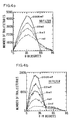
- Figs. 4a - 4d illustrate the effect of pressure on the angular distribution of sputtered particles arriving at the surface of a workpiece without a collimation filter and for three filters of different aspect ratios.
- the angle of arrival (0) relative to the perpendicular, is plotted along the x- axis and the number of particles arriving at the surface is plotted along the y-axis.
- the date for these figures was obtained by computer simulation assuming uniform erosion from a 28cm planar source, with a 150mm substrate and a 9cm source-to-substrate spacing in the Argon sputtering of aluminium. (The validity of the data obtained by computer simulation has since been confirmed in actual experiments).
- the particle count is arbitrary and was selected to be large enough to give meaningful distribution date.
- the same overall particle count was used in each of the simulations so that the relative reduction in particles reaching the substrate in successive figures reflects the higher percentage of material that is intercepted by the filter and, thus, not deposited.
- Figs. 4a - 4d curves representing the distributions for operating pressures of .00006Pa, .003Pa, .06Pa, and .13Pa are shown, and in Figs. 4b - 4d a curve for a pressure of 0.26Pa is also shown.
- Fig. 4a shows the distribution with no filter
- Figs. 4b - 4d show the distributions with filters having aspect ratios of 1:1, 1.5:1 and 2:1 respectively.
- the distribution is fairly symmetrical at the lower pressures for angles up to about 60 degrees. At the higher pressures, the distribution is less symmetrical, and greater relative numbers of the particles arrive at angles greater than 60 degrees.
- the distribution is fairly symmetrical at the lower pressures up to the acceptance angle of the filter.
- the distribution is less symmetrical, and greater relative numbers of the particles arrive at angles greater than the acceptance angle.
- the increase in the number of particles outside the acceptance angle at the higher pressures is due to scattering of the particles at the higher pressures after they transit the collimation filter.
- Figs. 6a - 6d illustrate the relationship between the initial deposition rate on the bottom wall and the aspect ratios or holes or vias and collimating filters.
- distance from the center of the hole or via expressed as a fraction of the radius of the hole or via is plotted along the x-axis, and the rate of deposition on the surface of the wafer is plotted along the y-axis.
- the target is assumed to be sufficiently large that the location of the opening on the wafer is unimportant.
- Curves are included for holes having aspect ratios ranging from 0.25:1 to 2:1.
- Fig. 6a shows the relationship without a collimating filter
- Figs. 6b - 6d show the relationship for f i lters having aspect ratios of 1:1, 2:1 and 4:1, respectively.
- the coating With no fitter and a hole having an aspect ratio of 1:1, the coating is full thickness toward the center of the opening but only about half thickness near the wall. With a filter having an aspect ratio of 1:1, the coating on the bottom wall is substantially more uniform, ranging from a normalized value of about .70 toward the center to about .40 near the wall. The bottom coating is even flatter with filters having aspect ratios of 2:1 and 4:1, but it is also substantially thinner.
- the bottom coating varies in thickness from a normalized value of about .60 toward the center to about .30 near the wall.
- the coating is more uniform, ranging from a normalized thickness of about .26 near the center to about .20 toward the wall.
- the coating is even more uniform, with a normalized thickness of about .13 from the center to the wall.
- Figs. 7a - 7b illustrate the formation of a step coating.
- Each of these figures shows a pair of holes 88, 89 having aspect ratios of 1:1, with hole 88 being located near the center of a wafer and hole 89 being toward the edge.
- Sputtering is performed at a pressure of 0.6Pa and a wafer table temperature of250°C, with a 28cm planar source, a 7cm target to wafer spacing, a collimation filter having an aspect ratio of 1:1, and a surface deposition rate of 1 micron per minute.
- Fig. 7a shows a half thickness coating of 0.5 micron on the wafer surface
- Fig. 7b shows a full thickness coating of 1 micron on the surface.
- the figures illustrate how the coating builds up evenly on the side walls of the openings without the overcoatng and asymmetry of the prior art techniques illustrated in Figs. 3a -3b.
- Another advantage which is apparent from these figures is that the thinnest part of the step coating is no longer at the lower corner of the hole as it is in the coatings of Figs, 3a - 3b. Film integrity at the corner of a via is especially important in obtaining a coating within the via having good, reliable electrical properties.
- the thinnest point occurs along the side wall, as indicated by the arrows 91, and with the full thickness coating, it occurs at the upper corner of the hole, as indicated by the arrows 92. From these figures, it can also be noted that the aspect ratio of the unfilled volume increases as the coating builds up in the holes.
- a titanium collimation filter is used in connection with sputtering from targets comprising titanium.
- the number of extraneous particles created when using a titanium collimation filter are greatly reduced from those of the prior art. Indeed, particle counts are such that sputtering of titanium compounds using a titanium collimation filter can be as clean or cleaner than the deposition of comparable materials by chemical vapor deposition (CVD).
- CVD chemical vapor deposition
- a collimator used in connection with a sputtering source is limited. As sputtering is performed, film is deposited on and builds up on the surfaces of the collimator, including the collimator cells. As the thickness of the coating on the cells increases, the deposition rate and properties of the sputtered film changes. Eventually, the collimator must be replaced. It has been found a collimator as described, which is matched in materials properties with the film being deposited, is usable over a normal life without any flaking.
- the extent of the benefit of using a compatible material to fabricate another component will depend on the amount of film which is deposited on the component as the sputtering system is used, since flaking occurs as film thickness increases.
- a collimation filter, or other component, which is placed directly between the sputter source and the workpiece, wi experience rapid film build up and, therefore, will begin flaking relatively quickly if there is a materials incompatibility problem.
- a cathode shield will experience little or no film deposition and, therefore, need not be made of a compatible material if doing so has any other disadvantages, such as higher manufacturing costs.
- the thermal coefficient of expansion (TCE) of both titanium and titanium nitride is 6.0. (This is expressed as 2.5 x of 10- s cms per cm degree Celsius. With titanium nitride a very low mismatch is essential due to the brittleness and low ductility of the film. Other films that are more ductile, or which have better adhesion characteristics, can tolerate a greater mismatch. For example, titanium tungsten alloy has a TCE of 3.0, yet adheres well to a titanium collimator. Likewise, aluminium, with a TCE of 13 adheres well to a stainless steel collimator (TCE of 9.9).
- Titanium has one additional property which makes it highly suitable for the present application: it tends to be an adsorber of gas. Many materials, including many metals, will “outgas” in a vacuum environment thereby introducing potentially contaminating substances into the process chamber. While such outgassing can be controlled by first "baking-out” the part to accelerate the outgassing, frequently it is not possible to bake out a part fully in a reasonable time- period, so that it remains a potential source of contamination. Moreover, even if baked out, the part may be recontaminated if it is subsequently exposed to the ambient atmosphere. Although load-locks are commonly used in sputtering equipment, the process chambers may be, nonetheless, frequently exposed to the atmosphere. This is not a problem with titanium, insofar as it tends not to outgas.
- the collimation filter has a thermal coefficient of expansion which closely matches that of the deposited film. It is preferred that the collimation filter should be made of a material which has excellent adherence qualities relative to the sputtered film; i.e., the bonding of forces between film and collimation filter are strong over the range of operating temperatures of the system.
Landscapes
- Chemical & Material Sciences (AREA)
- Engineering & Computer Science (AREA)
- Organic Chemistry (AREA)
- Materials Engineering (AREA)
- Mechanical Engineering (AREA)
- Metallurgy (AREA)
- Chemical Kinetics & Catalysis (AREA)
- Physics & Mathematics (AREA)
- Plasma & Fusion (AREA)
- Analytical Chemistry (AREA)
- Physical Vapour Deposition (AREA)
- Physical Deposition Of Substances That Are Components Of Semiconductor Devices (AREA)
- Electrodes Of Semiconductors (AREA)
Applications Claiming Priority (2)
| Application Number | Priority Date | Filing Date | Title |
|---|---|---|---|
| US99228592A | 1992-12-16 | 1992-12-16 | |
| US992285 | 1997-12-17 |
Publications (2)
| Publication Number | Publication Date |
|---|---|
| EP0606745A1 true EP0606745A1 (de) | 1994-07-20 |
| EP0606745B1 EP0606745B1 (de) | 1998-09-16 |
Family
ID=25538139
Family Applications (1)
| Application Number | Title | Priority Date | Filing Date |
|---|---|---|---|
| EP93310163A Expired - Lifetime EP0606745B1 (de) | 1992-12-16 | 1993-12-16 | Magnetronzerstäubungsgerät mit Kollimator für die Beschichtung eines Substrats |
Country Status (5)
| Country | Link |
|---|---|
| EP (1) | EP0606745B1 (de) |
| JP (1) | JPH07221019A (de) |
| KR (1) | KR100345253B1 (de) |
| CA (1) | CA2111536A1 (de) |
| DE (1) | DE69321095D1 (de) |
Cited By (5)
| Publication number | Priority date | Publication date | Assignee | Title |
|---|---|---|---|---|
| WO1996024155A1 (en) * | 1995-02-01 | 1996-08-08 | Advanced Micro Devices, Inc. | Multiple tier collimator system for enhanced step coverage and uniformity |
| WO1998020184A1 (en) * | 1996-11-04 | 1998-05-14 | Sola International Holdings Ltd. | Sputter coating apparatus |
| RU2160323C2 (ru) * | 1998-02-19 | 2000-12-10 | Иркутский государственный педагогический университет | Установка для ионно-плазменного распыления |
| EP2211367A1 (de) * | 2009-01-21 | 2010-07-28 | Applied Materials, Inc. | Teilchenstrahlvorrichtung mit verringerter Emission von ungewünschtem Material |
| CN115572949A (zh) * | 2022-09-16 | 2023-01-06 | 广州湾区半导体产业集团有限公司 | 一种双镀源物理气相沉积工艺及多模式物理气相沉积设备 |
Families Citing this family (4)
| Publication number | Priority date | Publication date | Assignee | Title |
|---|---|---|---|---|
| DE10004824B4 (de) * | 2000-02-04 | 2009-06-25 | Oc Oerlikon Balzers Ag | Verfahren zur Herstellung von Substraten, Magnetronquelle, Sputterbeschichtungskammer und Verwendung des Verfahrens |
| WO2013024915A1 (ko) * | 2011-08-17 | 2013-02-21 | 삼성전자주식회사 | 발광 소자의 투과성 전도막 형성을 위한 스퍼터링 장치 및 방법 |
| KR102647861B1 (ko) * | 2018-03-16 | 2024-03-18 | 삼성전자주식회사 | 콜리메이터, 그를 포함하는 반도체 소자의 제조장치 및 반도체 소자의 제조방법 |
| US11017989B2 (en) | 2018-03-16 | 2021-05-25 | Samsung Electronics Co., Ltd. | Collimator, fabrication apparatus including the same, and method of fabricating a semiconductor device using the same |
Citations (6)
| Publication number | Priority date | Publication date | Assignee | Title |
|---|---|---|---|---|
| EP0313750A1 (de) * | 1987-10-29 | 1989-05-03 | International Business Machines Corporation | Magnetron-Bedampfungssystem zum Ätzen oder Niederschlagen |
| EP0440377A2 (de) * | 1990-01-29 | 1991-08-07 | Varian Associates, Inc. | Gerät und Verfahren zur Niederschlagung durch einen Kollimator |
| EP0509305A1 (de) * | 1991-04-19 | 1992-10-21 | International Business Machines Corporation | Niederschlagsverfahren von Leitern in Öffnungen die tiefer als breit sind |
| EP0512296A1 (de) * | 1991-04-19 | 1992-11-11 | Siemens Aktiengesellschaft | Hochtemperatur-Niederschlagsverfahren von Leitern in Öffnungen, die tiefer als breit sind |
| US5223108A (en) * | 1991-12-30 | 1993-06-29 | Materials Research Corporation | Extended lifetime collimator |
| US5252194A (en) * | 1990-01-26 | 1993-10-12 | Varian Associates, Inc. | Rotating sputtering apparatus for selected erosion |
Family Cites Families (1)
| Publication number | Priority date | Publication date | Assignee | Title |
|---|---|---|---|---|
| JPS6229133A (ja) * | 1985-07-31 | 1987-02-07 | Hitachi Ltd | スパツタ方法およびその装置 |
-
1993
- 1993-12-15 CA CA002111536A patent/CA2111536A1/en not_active Abandoned
- 1993-12-16 JP JP5343556A patent/JPH07221019A/ja active Pending
- 1993-12-16 DE DE69321095T patent/DE69321095D1/de not_active Expired - Lifetime
- 1993-12-16 EP EP93310163A patent/EP0606745B1/de not_active Expired - Lifetime
- 1993-12-16 KR KR1019930027964A patent/KR100345253B1/ko not_active Expired - Fee Related
Patent Citations (6)
| Publication number | Priority date | Publication date | Assignee | Title |
|---|---|---|---|---|
| EP0313750A1 (de) * | 1987-10-29 | 1989-05-03 | International Business Machines Corporation | Magnetron-Bedampfungssystem zum Ätzen oder Niederschlagen |
| US5252194A (en) * | 1990-01-26 | 1993-10-12 | Varian Associates, Inc. | Rotating sputtering apparatus for selected erosion |
| EP0440377A2 (de) * | 1990-01-29 | 1991-08-07 | Varian Associates, Inc. | Gerät und Verfahren zur Niederschlagung durch einen Kollimator |
| EP0509305A1 (de) * | 1991-04-19 | 1992-10-21 | International Business Machines Corporation | Niederschlagsverfahren von Leitern in Öffnungen die tiefer als breit sind |
| EP0512296A1 (de) * | 1991-04-19 | 1992-11-11 | Siemens Aktiengesellschaft | Hochtemperatur-Niederschlagsverfahren von Leitern in Öffnungen, die tiefer als breit sind |
| US5223108A (en) * | 1991-12-30 | 1993-06-29 | Materials Research Corporation | Extended lifetime collimator |
Non-Patent Citations (1)
| Title |
|---|
| & EP-A-0 439 360 * |
Cited By (7)
| Publication number | Priority date | Publication date | Assignee | Title |
|---|---|---|---|---|
| WO1996024155A1 (en) * | 1995-02-01 | 1996-08-08 | Advanced Micro Devices, Inc. | Multiple tier collimator system for enhanced step coverage and uniformity |
| US5643428A (en) * | 1995-02-01 | 1997-07-01 | Advanced Micro Devices, Inc. | Multiple tier collimator system for enhanced step coverage and uniformity |
| WO1998020184A1 (en) * | 1996-11-04 | 1998-05-14 | Sola International Holdings Ltd. | Sputter coating apparatus |
| RU2160323C2 (ru) * | 1998-02-19 | 2000-12-10 | Иркутский государственный педагогический университет | Установка для ионно-плазменного распыления |
| EP2211367A1 (de) * | 2009-01-21 | 2010-07-28 | Applied Materials, Inc. | Teilchenstrahlvorrichtung mit verringerter Emission von ungewünschtem Material |
| CN115572949A (zh) * | 2022-09-16 | 2023-01-06 | 广州湾区半导体产业集团有限公司 | 一种双镀源物理气相沉积工艺及多模式物理气相沉积设备 |
| CN115572949B (zh) * | 2022-09-16 | 2023-06-16 | 广州湾区半导体产业集团有限公司 | 一种双镀源物理气相沉积工艺及多模式物理气相沉积设备 |
Also Published As
| Publication number | Publication date |
|---|---|
| JPH07221019A (ja) | 1995-08-18 |
| CA2111536A1 (en) | 1994-06-17 |
| KR100345253B1 (ko) | 2002-11-23 |
| DE69321095D1 (de) | 1998-10-22 |
| KR940016462A (ko) | 1994-07-23 |
| EP0606745B1 (de) | 1998-09-16 |
Similar Documents
| Publication | Publication Date | Title |
|---|---|---|
| US5330628A (en) | Collimated deposition apparatus and method | |
| US5650052A (en) | Variable cell size collimator | |
| EP0809859B1 (de) | Aus mehreren lagen bestehende kollimatoranordnung für verbesserte höhenunterschiedbeschichtung und gleichmässigkeit | |
| US5635036A (en) | Collimated deposition apparatus and method | |
| US6328858B1 (en) | Multi-layer sputter deposition apparatus | |
| US5584973A (en) | Processing apparatus with an invertible collimator and a processing method therefor | |
| EP1746181A2 (de) | Verbesserte Magnetron Zerstäubungsvorrichtung zur Behandlung grossflächiger Substrate | |
| KR101364764B1 (ko) | 도전성 페이스팅 재료의 증착 장치 및 방법 | |
| JPH0860355A (ja) | 処理装置 | |
| JP2000144399A (ja) | スパッタリング装置 | |
| WO2000018979A9 (en) | Sputter deposition apparatus | |
| KR20210052600A (ko) | 웨이퍼 프로세싱 증착 차폐 부품 | |
| EP0606745B1 (de) | Magnetronzerstäubungsgerät mit Kollimator für die Beschichtung eines Substrats | |
| EP0363673B1 (de) | Durch Zerstäubung abgeschiedene Nickelschicht und Verfahren zu deren Abscheidung | |
| TW202321484A (zh) | 具有旋轉底座的傾斜pvd源 | |
| US6521106B1 (en) | Collimated deposition apparatus | |
| TW202426673A (zh) | 用於在基板上沉積材料之系統與方法 | |
| US4416760A (en) | Apparatus for asymmetrically contouring the thickness of sputter coated layers | |
| KR100270460B1 (ko) | 스퍼터링장치 | |
| US20060081466A1 (en) | High uniformity 1-D multiple magnet magnetron source | |
| TW202436650A (zh) | 用於在通孔內沉積材料的裝置和方法 | |
| JPH0360916B2 (de) | ||
| CN117026188B (zh) | 一种磁控溅射复合镀膜方法 | |
| US20260049393A1 (en) | Physical vapor deposition module and system including same | |
| JPS6277477A (ja) | 薄膜形成装置 |
Legal Events
| Date | Code | Title | Description |
|---|---|---|---|
| PUAI | Public reference made under article 153(3) epc to a published international application that has entered the european phase |
Free format text: ORIGINAL CODE: 0009012 |
|
| AK | Designated contracting states |
Kind code of ref document: A1 Designated state(s): CH DE FR GB LI NL |
|
| 17P | Request for examination filed |
Effective date: 19941216 |
|
| 17Q | First examination report despatched |
Effective date: 19960514 |
|
| GRAG | Despatch of communication of intention to grant |
Free format text: ORIGINAL CODE: EPIDOS AGRA |
|
| GRAG | Despatch of communication of intention to grant |
Free format text: ORIGINAL CODE: EPIDOS AGRA |
|
| GRAH | Despatch of communication of intention to grant a patent |
Free format text: ORIGINAL CODE: EPIDOS IGRA |
|
| GRAH | Despatch of communication of intention to grant a patent |
Free format text: ORIGINAL CODE: EPIDOS IGRA |
|
| GRAA | (expected) grant |
Free format text: ORIGINAL CODE: 0009210 |
|
| AK | Designated contracting states |
Kind code of ref document: B1 Designated state(s): CH DE FR GB LI NL |
|
| PG25 | Lapsed in a contracting state [announced via postgrant information from national office to epo] |
Ref country code: NL Free format text: LAPSE BECAUSE OF FAILURE TO SUBMIT A TRANSLATION OF THE DESCRIPTION OR TO PAY THE FEE WITHIN THE PRESCRIBED TIME-LIMIT Effective date: 19980916 Ref country code: LI Free format text: LAPSE BECAUSE OF FAILURE TO SUBMIT A TRANSLATION OF THE DESCRIPTION OR TO PAY THE FEE WITHIN THE PRESCRIBED TIME-LIMIT Effective date: 19980916 Ref country code: FR Free format text: LAPSE BECAUSE OF FAILURE TO SUBMIT A TRANSLATION OF THE DESCRIPTION OR TO PAY THE FEE WITHIN THE PRESCRIBED TIME-LIMIT Effective date: 19980916 Ref country code: CH Free format text: LAPSE BECAUSE OF FAILURE TO SUBMIT A TRANSLATION OF THE DESCRIPTION OR TO PAY THE FEE WITHIN THE PRESCRIBED TIME-LIMIT Effective date: 19980916 |
|
| REG | Reference to a national code |
Ref country code: CH Ref legal event code: EP |
|
| REF | Corresponds to: |
Ref document number: 69321095 Country of ref document: DE Date of ref document: 19981022 |
|
| PG25 | Lapsed in a contracting state [announced via postgrant information from national office to epo] |
Ref country code: DE Free format text: LAPSE BECAUSE OF FAILURE TO SUBMIT A TRANSLATION OF THE DESCRIPTION OR TO PAY THE FEE WITHIN THE PRESCRIBED TIME-LIMIT Effective date: 19981217 |
|
| EN | Fr: translation not filed | ||
| NLV1 | Nl: lapsed or annulled due to failure to fulfill the requirements of art. 29p and 29m of the patents act | ||
| REG | Reference to a national code |
Ref country code: CH Ref legal event code: PL |
|
| PLBE | No opposition filed within time limit |
Free format text: ORIGINAL CODE: 0009261 |
|
| STAA | Information on the status of an ep patent application or granted ep patent |
Free format text: STATUS: NO OPPOSITION FILED WITHIN TIME LIMIT |
|
| 26N | No opposition filed | ||
| REG | Reference to a national code |
Ref country code: GB Ref legal event code: IF02 |
|
| PGFP | Annual fee paid to national office [announced via postgrant information from national office to epo] |
Ref country code: GB Payment date: 20050119 Year of fee payment: 12 |
|
| PG25 | Lapsed in a contracting state [announced via postgrant information from national office to epo] |
Ref country code: GB Free format text: LAPSE BECAUSE OF NON-PAYMENT OF DUE FEES Effective date: 20051216 |
|
| GBPC | Gb: european patent ceased through non-payment of renewal fee |
Effective date: 20051216 |