EP0607501A2 - Amélioration de, ou en relation avec, des couches minces en matériaux ferroélectriques - Google Patents
Amélioration de, ou en relation avec, des couches minces en matériaux ferroélectriques Download PDFInfo
- Publication number
- EP0607501A2 EP0607501A2 EP93115623A EP93115623A EP0607501A2 EP 0607501 A2 EP0607501 A2 EP 0607501A2 EP 93115623 A EP93115623 A EP 93115623A EP 93115623 A EP93115623 A EP 93115623A EP 0607501 A2 EP0607501 A2 EP 0607501A2
- Authority
- EP
- European Patent Office
- Prior art keywords
- grain size
- perovskite material
- donor
- pyroelectric
- layer
- Prior art date
- Legal status (The legal status is an assumption and is not a legal conclusion. Google has not performed a legal analysis and makes no representation as to the accuracy of the status listed.)
- Withdrawn
Links
Images
Classifications
-
- H—ELECTRICITY
- H10—SEMICONDUCTOR DEVICES; ELECTRIC SOLID-STATE DEVICES NOT OTHERWISE PROVIDED FOR
- H10N—ELECTRIC SOLID-STATE DEVICES NOT OTHERWISE PROVIDED FOR
- H10N15/00—Thermoelectric devices without a junction of dissimilar materials; Thermomagnetic devices, e.g. using the Nernst-Ettingshausen effect
- H10N15/10—Thermoelectric devices using thermal change of the dielectric constant, e.g. working above and below the Curie point
- H10N15/15—Thermoelectric active materials
-
- C—CHEMISTRY; METALLURGY
- C04—CEMENTS; CONCRETE; ARTIFICIAL STONE; CERAMICS; REFRACTORIES
- C04B—LIME, MAGNESIA; SLAG; CEMENTS; COMPOSITIONS THEREOF, e.g. MORTARS, CONCRETE OR LIKE BUILDING MATERIALS; ARTIFICIAL STONE; CERAMICS; REFRACTORIES; TREATMENT OF NATURAL STONE
- C04B35/00—Shaped ceramic products characterised by their composition; Ceramics compositions; Processing powders of inorganic compounds preparatory to the manufacturing of ceramic products
- C04B35/01—Shaped ceramic products characterised by their composition; Ceramics compositions; Processing powders of inorganic compounds preparatory to the manufacturing of ceramic products based on oxide ceramics
- C04B35/46—Shaped ceramic products characterised by their composition; Ceramics compositions; Processing powders of inorganic compounds preparatory to the manufacturing of ceramic products based on oxide ceramics based on titanium oxides or titanates
- C04B35/462—Shaped ceramic products characterised by their composition; Ceramics compositions; Processing powders of inorganic compounds preparatory to the manufacturing of ceramic products based on oxide ceramics based on titanium oxides or titanates based on titanates
- C04B35/465—Shaped ceramic products characterised by their composition; Ceramics compositions; Processing powders of inorganic compounds preparatory to the manufacturing of ceramic products based on oxide ceramics based on titanium oxides or titanates based on titanates based on alkaline earth metal titanates
Definitions
- This invention generally relates to the fabrication of thin film ferroelectric materials such as those used in non-volatile memory device.
- the class of materials known as the perovskites exhibit several properties which make them useful in the microeletronics industry. Among these properties is a dielectric constant which can be several orders of magnitude greater than that of conventional insulators used in integrated circuits (e.g. SiO2 and Si3N4). This high dielectric constant can allow fabrication of very small capacitors which store charge in conventional DRAMs (dynamic random access memories), thereby increasing the density of memory cells.
- a dielectric constant which can be several orders of magnitude greater than that of conventional insulators used in integrated circuits (e.g. SiO2 and Si3N4). This high dielectric constant can allow fabrication of very small capacitors which store charge in conventional DRAMs (dynamic random access memories), thereby increasing the density of memory cells.
- the pyroelectric FOM is proportional to the ratio between the pyroelectric coefficient and dielectric constant.
- the pyroelectric coefficient is a function of the dielectric constant and the spontaneous polarization.
- Many perovskites exhibit a very large pyroelectric FOM, and if sufficiently large this pyroelectric property makes possible devices which are very sensitive to changes in temperature, including temperature changes caused by impinging electromagnetic radiation.
- Arrays of such pyroelectric detectors are now being fabricated which can image an infrared scene. These detectors do not require cryogenic cooling and are therefore economically feasible for consumer applications.
- the ferroelectric properties of perovskite materials are also useful in the microelectronics industry. Among those properties is the remanent polarization. The direction of this polarization may be switched by the application of an electric field to the material. The polarization remains after the electric field is removed. The direction of this polarization may then be sensed electronically.
- FRAMs ferrroelectric random access memories
- Such devices depending on the configuration, could in addition exhibit faster read/write cycles than conventional DRAMs.
- This invention is a method of forming thin-film perovskite structures which exhibit useful ferroelectric and pyroelectric properties.
- the perovskite materials are (1) any material exhibiting the well known perovskite crystal structure, typified by CaTiO3; and (2) compounds with structures which can be derived from the ideal cubic perovskite structure by way of small lattice distortions or omission of some atoms.
- Many perovskites have the chemical formula ABO3, where A is one or more monovalent, divalent or trivalent elements and B is one or more pentavalent, tetravalent, trivalent or divalent elements.
- perovskite materials To be useful in the fabrication of integrated circuit FRAMs, perovskite materials must exhibit large remanent polarization and small coercive voltage. To be useful in the fabrication of thin-film pyroelectric devices, perovskite materials must exhibit a large pyroelectric FOM. These properties should be present in thin-films of these materials.
- perovskite materials generally decrease as the grain size of the material is decreased.
- Bulk ceramic forms of perovskites generally have grain sizes on the order of 0.5 - 100 micrometers ( ⁇ m), whereas typical thin-films have grain sizes of 0.02 - 0.5 ⁇ m.
- the useful properties are essentially absent for grain sizes below a critical grain size which is unique for each material and property.
- the precise composition of perovskites also affects their ferroelectric and pyroelectric properties.
- Changing the composition of perovskites is another technique which has been used to preserve ferroelectric and pyroelectric properties in thin films.
- the ferroelectric properties of some lead containing perovskites do not decrease as rapidly with decreasing grain size.
- PbO is very reactive with many materials, is easily chemically reduced, has a large vapor pressure and readily poisons silicon devices. For these reasons such materials are probably inappropriate candidates for use in the fabrication of integrated circuits.
- this invention overcomes the tradeoffs inherent in prior art techniques by doping the material in a way that decreases the grain size at which ferroelectric and/or pyroelectric properties abate.
- the ferroelectric properties (i.e. remanent polarization) of thin film perovskite materials are enhanced by doping.
- the embodiment described is a method of forming an improved ferroelectric material by doping an intrinsic perovskite material having an intrinsic ferroelectric critical grain size with one or more donor dopants, then forming a layer of the donor doped perovskite material having an average grain size less than the intrinsic ferroelectric critical grain size whereby the remanent polarization of the layer is substantially greater than the remanent polarization of the intrinsic perovskite material with an average grain size similar to the average grain size of the layer.
- the ferroelectric critical grain size as used herein, means the largest grain size such that the remanent polarization starts to rapidly decrease with decreasing grain sizes.
- the donor doped perovskites material is further doped with one or more acceptor dopants to form a donor-acceptor doped perovskite material whereby the resistivity is substantially increased.
- the intrinsic perovskite material has a chemical composition ABO3, where A is one or more monovalent, divalent or trivalent elements, and B is one or more pentavalent, tetravalent, trivalent or divalent elements.
- the pyroelectric properties (i.e. pyroelectric FOM) of thin film perovskites materials are enhanced by doping.
- the invention described is a method of forming an improved pyroelectric material by doping an intrinsic perovskite material having an intrinsic pyroelectric critical grain size with one or more donor dopants, then forming a layer of the donor doped perovskite material having an average grain size less than the intrinsic pyroelectric critical grain size whereby the pyroelectric FOM of the layer is substantially greater than the pyroelectric FOM of the intrinsic perovskite material with an average grain size similar to the average grain size of the layer.
- the pyroelectric critical grain size means the largest grain size such that the pyroelectric FOM starts to rapidly decrease with decreasing grain sizes.
- the donor doped perovskite material is further doped with one or more acceptor dopants to form a donor-acceptor doped perovskite material whereby the resistivity is substantially increased.
- the intrinsic perovskite material has a chemical composition ABO3, where A is one or more monovalent, divalent or trivalent elements, and B is one or more pentavalent, tetravalent, trivalent or divalent elements.
- Structures containing these improved ferroelectric and pyroelectric materials include a layer of donor doped perovskite material with average grain size less than the intrinsic ferroelectric or pyroelectric critical grain size formed on the surface of a substrate.
- Other structures include such a layer of donor doped material interposed between two electrically conducting layers.
- the applications of this invention are many.
- the materials presented may find use in many structures used in semiconductor circuitry, such as capacitors, transistors, non-volatile memory cells, pixels for electro-magnetic radiation detecting arrays, and other electrooptic applications. Devices which exploit the piezoelectric properties of many of these materials will benefit from this invention.
- the advantages of this invention include substantially increased remanent polarization for perovskite materials formed with grain sizes typically found in thin films. This invention also serves to preserve the pyroelectric FOM in thin films of perovskite materials. In addition, the resistivity is generally increased by the methods presented.
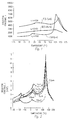
- the useful ferroelectric and pyroelectric properties of a perovskite material generally decrease as the grain size of the material is decreased.
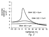
- the dielectric constant of undoped barium titanate (BT) varies with temperature and grain size.
- the dielectric constant varies rapidly near the Curie temperature (approximately 130 °C), but is less variable at other temperatures.
- the peak becomes less pronounced, the dielectric constant below the Curie temperature increases and varies less with temperature.
- the dielectric constant decreases for all temperatures and is essentially constant with respect to temperature.
- the dielectric constant has a pronounced peak at the Curie temperature. As the grain size decreases, the dielectric constant below the Curie temperature increases and the peak is less pronounced.
- the rate of change of the dielectric constant with temperature is large, the pyroelectric FOM is also large.
- the rate of change of the dielectric constant decreases below some grain size, i.e. the slope of the curve becomes smaller as the grain size is decreased below some value.
- That value for barium titanate is approximately 6.8 ⁇ m according to the data represented by Figure 1.
- Figure 3 illustrates, that value for barium strontium titanate is approximately 10 ⁇ m.
- the pyroelectric FOM of pyroelectric perovskite materials decreases rapidly below some grain size.
- the pyroelectric critical grain size means the largest grain size such that the pyroelectric FOM starts to rapidly decrease with decreasing grain sizes.
- the typical grain size present in most thin-film perovskites is generally much smaller than the PCGS, causing the pyroelectric properties of thin films to be small or nonexistent.
- the grain size of a thin film perovskite must be larger than the PCGS in order for the film to possess useful pyroelectric properties. A method to decrease the PCGS below typical thin film grain sizes is desirable.
- the useful ferroelectric properties of perovskites also decrease for decreasing grain sizes.
- the remanent polarization exhibited by barium zirconate titanate is 18 ⁇ C/cm2 for grain sizes larger than 100 ⁇ m.
- the remanent polarization has been measured at 6 ⁇ C/cm2.
- the remanent polarization rapidly decreases until it is essentially gone.
- the remanent polarization of ferroelectric perovskites materials decreases rapidly below some grain size.
- the ferroelectric critical grain size means the largest grain size such that the remanent polarization starts to rapidly decrease with decreasing grain sizes.
- the typical grain size present in most thin-film perovskites is generally much smaller than the FCGS, causing the ferroelectric properties of thin films to be small or nonexistent.
- the grain size of a thin film perovskite must be larger than the FCGS in order for the film to possess useful ferroelectric properties. A method to decrease the FCGS below typical thin film grain sizes is desirable.
- donor dopants generally decrease the pyroelectric critical grain size and the ferroelectric critical grain size of perovskite materials. This effect is not taught by the prior art and its mechanism and explanation are uncertain.
- an element or ion is a donor dopant if (1) it replaces an atom in the crystal lattice and has a greater number of valence electrons than the atom it replaces or (2) it exists interstitially and its outer electron shell is less than half full.
- Intermediate cases are uncertain and may be determined empirically. For example, some elements behave as donor dopants in (1) when their valence is the same as the atom replaced. Likewise, in (2) some element behave as donor dopants when their valence shell is exactly half full.
- acceptor dopants increase the resistivity of some perovskite materials. Therefore, another aspect of this invention is acceptor co-doping of ferroelectric and pyroelectric perovskite materials.
- an element or ion is an acceptor dopant if (1) it replaces an atom in the crystal lattice and has a lesser number of valence electrons than the atom it replaces or (2) it exists interstitially and its outer electron shell is more than half full. Intermediate cases are uncertain and may be determined empirically. For example, some elements behave as acceptor dopants in (1) when their valence is the same as the atom replaced Likewise, in (2) some elements behave as acceptor dopants when their valence shell is exactly half full.
- a dopant is a species which is intentionally introduced into an intrinsic material in order to produce some effect. Unintentional impurities which exist in concentrations below approximately 0.1 mole percent are not generally considered dopants. Accordingly, in the context of this invention, an intrinsic perovskite material is a perovskite material in which impurities which behave as donor or acceptor dopants, if present, exist at concentrations below approximately 0.1 mole percent. Similarly, an intrinsic pyroelectric critical grain size (IPCGS) is the pyroelectric critical grain size of an intrinsic perovskite material. An intrinsic ferroelectric critical grain size (IFCGS) is the ferroelectric critical grain size of an intrinsic perovskite material.
- the nominal compositional formula for the preferred embodiment material is given as (Ba a ,Sr b ,Ca c ) 1-x D x Ti 1-y A y O3
- D comprises a trivalent donor ion (e.g., Bi, Sb, Y, La, Ce, Pr, Nd, Sm, Gd, Tb, Dy, Ho, and Er or a combination thereof) and
- A comprises a trivalent acceptor ion (e.g., Co, Cu, Fe, Mn Ru, Al, Ga, Sc, In, Ni, and Yb or a combination thereof) or a divalent acceptor ion (e.g., Mg).
- both trivalent and divalent acceptor ions reside on the Ti sub-lattice.
- Table 1 The values for the compositional ratios are given in Table 1, below.
- the nominal compositional formula for a second preferred embodiment material is given as (Ba a ,Sr b ,Ca c )Ti 1-x-y D x A y O3 where D comprises a pentavalent donor ion (e.g., Nb, Ta or a combination thereof) and A comprises a trivalent or divalent acceptor ion (e.g., Co, Cu, Fe, Mn, Ru, Al, Ga, Mg, Sc, In, Ni, and Yb or a combination thereof).
- D comprises a pentavalent donor ion (e.g., Nb, Ta or a combination thereof)
- A comprises a trivalent or divalent acceptor ion (e.g., Co, Cu, Fe, Mn, Ru, Al, Ga, Mg, Sc, In, Ni, and Yb or a combination thereof).
- the values for the compositional ratios given in Table 1 still apply.
- the nominal compositional formula for a third preferred embodiment material is given as (Ba a ,Sr b ,Ca c ) 1-x-y D x A y TiO3 where D comprises a trivalent donor ion (e.g., Bi, Sb, Y, La, Ce, Pr, Nd, Sm, Gd, Tb, Dy, Ho, and Er or a combination thereof) and A comprises a univalent acceptor ion (e.g., K, Na or a combination thereof).
- a trivalent donor ion e.g., Bi, Sb, Y, La, Ce, Pr, Nd, Sm, Gd, Tb, Dy, Ho, and Er or a combination thereof
- A comprises a univalent acceptor ion (e.g., K, Na or a combination thereof).
- the nominal compositional formula for a fourth preferred embodiment material is given as (Ba a ,Sr b ,Ca c ) 1-y A y Ti 1-x D x O3 where D comprises a pentavalent donor ion (e.g., Nb, Ta, or a combination thereof) and A comprises a univalent acceptor ion (e.g., K, Na or a combination thereof). Yet once again, the values for the compositional ratios given in Table 1 apply.
- material with the nominal composition Ba 0.66 ,Sr 0.34 ,Dy 0.01 )Ti 1.009 Mn 0.001 O 3.03 was prepared.
- the material was made by combining constituents in a solution, then the solution was calcined in bulk, ground, pressed, then sintered. The resulting ceramic density was at least 95% of theoretical density.
- the ceramic material was then mechanically polished and thinned to 250 ⁇ m thickness.
- Metallization was applied to form test capacitors.
- the average grain size of this material was 0.5 ⁇ m as measured by the line intercept method.
- the peak dielectric constant (the dielectric constant at the Curie temperature) was greater than 10,000, and varied rapidly with respect to temperature (i.e. this material exhibited good pyroelectric properties). This behavior indicates that the pyroelectric critical grain size of this material is less than 0.5 ⁇ m.
- Internal and external connections can be ohmic, capacitive, direct or indirect, via intervening circuits or otherwise. Implementation is contemplated in discrete components or fully integrated circuits in silicon, gallium arsenide, or other electronic materials families, as well as in optical-based or other technology-based forms and embodiments.
Landscapes
- Engineering & Computer Science (AREA)
- Chemical & Material Sciences (AREA)
- Ceramic Engineering (AREA)
- Manufacturing & Machinery (AREA)
- Materials Engineering (AREA)
- Structural Engineering (AREA)
- Organic Chemistry (AREA)
- Inorganic Insulating Materials (AREA)
- Semiconductor Integrated Circuits (AREA)
- Semiconductor Memories (AREA)
- Inorganic Compounds Of Heavy Metals (AREA)
- Other Surface Treatments For Metallic Materials (AREA)
Applications Claiming Priority (2)
| Application Number | Priority Date | Filing Date | Title |
|---|---|---|---|
| US95159692A | 1992-09-28 | 1992-09-28 | |
| US951596 | 1992-09-28 |
Publications (2)
| Publication Number | Publication Date |
|---|---|
| EP0607501A2 true EP0607501A2 (fr) | 1994-07-27 |
| EP0607501A3 EP0607501A3 (fr) | 1995-06-07 |
Family
ID=25491887
Family Applications (1)
| Application Number | Title | Priority Date | Filing Date |
|---|---|---|---|
| EP93115623A Withdrawn EP0607501A3 (fr) | 1992-09-28 | 1993-09-28 | Amélioration de, ou en relation avec, des couches minces en matériaux ferroélectriques. |
Country Status (4)
| Country | Link |
|---|---|
| EP (1) | EP0607501A3 (fr) |
| JP (1) | JPH0722593A (fr) |
| KR (1) | KR100311335B1 (fr) |
| MX (1) | MX9305897A (fr) |
Families Citing this family (3)
| Publication number | Priority date | Publication date | Assignee | Title |
|---|---|---|---|---|
| JP2000189453A (ja) | 1998-12-28 | 2000-07-11 | Nichiban Co Ltd | 医療用粘着テ―プ |
| KR20010017099A (ko) * | 1999-08-07 | 2001-03-05 | 심상기 | 수세미 편직기 |
| JP4218184B2 (ja) | 2000-05-19 | 2009-02-04 | 株式会社デンソー | 半導体装置の実装構造 |
Family Cites Families (2)
| Publication number | Priority date | Publication date | Assignee | Title |
|---|---|---|---|---|
| DE2308073B2 (de) * | 1973-02-19 | 1976-09-02 | Siemens AG, 1000 Berlin und 8000 München | Keramischer elektrischer widerstandskoerper mit positivem temperaturkoeffizienten des elektrischen widerstandswertes und verfahren zu seiner herstellung |
| SU1004314A1 (ru) * | 1980-12-09 | 1983-03-15 | Предприятие П/Я Г-4816 | Сегнетоэлектрический керамический материал |
-
1993
- 1993-09-24 MX MX9305897A patent/MX9305897A/es unknown
- 1993-09-25 KR KR1019930019705A patent/KR100311335B1/ko not_active Expired - Fee Related
- 1993-09-27 JP JP5240104A patent/JPH0722593A/ja active Pending
- 1993-09-28 EP EP93115623A patent/EP0607501A3/fr not_active Withdrawn
Also Published As
| Publication number | Publication date |
|---|---|
| EP0607501A3 (fr) | 1995-06-07 |
| KR940008078A (ko) | 1994-04-28 |
| JPH0722593A (ja) | 1995-01-24 |
| MX9305897A (es) | 1994-07-29 |
| KR100311335B1 (ko) | 2001-12-15 |
Similar Documents
| Publication | Publication Date | Title |
|---|---|---|
| US5760432A (en) | Thin film strained layer ferroelectric capacitors | |
| Naoko Yanase et al. | Thickness dependence of ferroelectricity in heteroepitaxial BaTiO3 thin film capacitors | |
| US6642539B2 (en) | Epitaxial template and barrier for the integration of functional thin film metal oxide heterostructures on silicon | |
| US11121139B2 (en) | Hafnium oxide and zirconium oxide based ferroelectric devices with textured iridium bottom electrodes | |
| KR100228038B1 (ko) | 박막캐패시터 | |
| US5418389A (en) | Field-effect transistor with perovskite oxide channel | |
| Ayyub et al. | Ferroelectric behavior in thin films of antiferroelectric materials | |
| US6060735A (en) | Thin film dielectric device | |
| EP0571948B1 (fr) | Perovskites dopés en donneurs pour couche mince diélectrique | |
| US5168420A (en) | Ferroelectrics epitaxially grown on superconducting substrates | |
| JPH10269842A (ja) | 導電性酸化物薄膜、薄膜キャパシタおよび磁気抵抗効果素子 | |
| US20100182730A1 (en) | Ferroelectric varactor with improved tuning range | |
| Zhang et al. | Characteristics of the electromechanical response and polarization of electric field biased ferroelectrics | |
| Guerrero et al. | Growth and characterization of epitaxial ferroelectric PbZrxTi1− xO3 thin film capacitors with SrRuO3 electrodes for non-volatile memory applications | |
| Udayakumar et al. | Polarization reversal and high dielectric permittivity in lead magnesium niobate titanate thin films | |
| Abe et al. | Modification of ferroelectricity in heteroepitaxial (Ba, Sr) TiO3 films for non-volatile memory applications | |
| JPH08335672A (ja) | 強誘電体不揮発性メモリ | |
| US5504330A (en) | Lead substitured perovskites for thin-film pyroelectric devices | |
| US5721043A (en) | Method of forming improved thin film dielectrics by Pb doping | |
| US5888659A (en) | Donor doped perovskites for thin-film ferroelectric and pyroelectric devices | |
| EP0607501A2 (fr) | Amélioration de, ou en relation avec, des couches minces en matériaux ferroélectriques | |
| US6432473B1 (en) | PB substituted perovskites for thin films dielectrics | |
| EP0661244A2 (fr) | Fabrication des matériaux à film mince | |
| JPH08330540A (ja) | 酸化物積層構造 | |
| JPH1187634A (ja) | 薄膜キャパシタ |
Legal Events
| Date | Code | Title | Description |
|---|---|---|---|
| PUAI | Public reference made under article 153(3) epc to a published international application that has entered the european phase |
Free format text: ORIGINAL CODE: 0009012 |
|
| AK | Designated contracting states |
Kind code of ref document: A2 Designated state(s): DE FR GB IT NL |
|
| PUAL | Search report despatched |
Free format text: ORIGINAL CODE: 0009013 |
|
| AK | Designated contracting states |
Kind code of ref document: A3 Designated state(s): DE FR GB IT NL |
|
| 17P | Request for examination filed |
Effective date: 19951124 |
|
| 17Q | First examination report despatched |
Effective date: 19960725 |
|
| STAA | Information on the status of an ep patent application or granted ep patent |
Free format text: STATUS: THE APPLICATION IS DEEMED TO BE WITHDRAWN |
|
| 18D | Application deemed to be withdrawn |
Effective date: 19980213 |