EP0607677A2 - Circuit intégré de mise en forme d'ondes - Google Patents
Circuit intégré de mise en forme d'ondes Download PDFInfo
- Publication number
- EP0607677A2 EP0607677A2 EP93310017A EP93310017A EP0607677A2 EP 0607677 A2 EP0607677 A2 EP 0607677A2 EP 93310017 A EP93310017 A EP 93310017A EP 93310017 A EP93310017 A EP 93310017A EP 0607677 A2 EP0607677 A2 EP 0607677A2
- Authority
- EP
- European Patent Office
- Prior art keywords
- signal
- logic
- delayed
- input
- pair
- Prior art date
- Legal status (The legal status is an assumption and is not a legal conclusion. Google has not performed a legal analysis and makes no representation as to the accuracy of the status listed.)
- Withdrawn
Links
- 230000000295 complement effect Effects 0.000 claims abstract description 164
- 230000003111 delayed effect Effects 0.000 claims description 263
- 230000004044 response Effects 0.000 claims description 97
- 230000007704 transition Effects 0.000 claims description 76
- 230000000630 rising effect Effects 0.000 claims description 25
- 239000003990 capacitor Substances 0.000 claims description 10
- 238000000034 method Methods 0.000 claims description 6
- 230000001934 delay Effects 0.000 claims description 2
- 230000003534 oscillatory effect Effects 0.000 claims 41
- 238000010586 diagram Methods 0.000 description 38
- 230000008859 change Effects 0.000 description 8
- 230000005540 biological transmission Effects 0.000 description 7
- 230000007423 decrease Effects 0.000 description 4
- PWWSSIYVTQUJQQ-UHFFFAOYSA-N distearyl thiodipropionate Chemical compound CCCCCCCCCCCCCCCCCCOC(=O)CCSCCC(=O)OCCCCCCCCCCCCCCCCCC PWWSSIYVTQUJQQ-UHFFFAOYSA-N 0.000 description 4
- 238000001914 filtration Methods 0.000 description 3
- XUIMIQQOPSSXEZ-UHFFFAOYSA-N Silicon Chemical compound [Si] XUIMIQQOPSSXEZ-UHFFFAOYSA-N 0.000 description 2
- 230000009471 action Effects 0.000 description 2
- 230000003247 decreasing effect Effects 0.000 description 2
- 230000001419 dependent effect Effects 0.000 description 2
- 238000009434 installation Methods 0.000 description 2
- 238000004519 manufacturing process Methods 0.000 description 2
- 230000008569 process Effects 0.000 description 2
- 229910052710 silicon Inorganic materials 0.000 description 2
- 239000010703 silicon Substances 0.000 description 2
- 230000001360 synchronised effect Effects 0.000 description 2
- 101150110971 CIN7 gene Proteins 0.000 description 1
- 101100286980 Daucus carota INV2 gene Proteins 0.000 description 1
- 101150110298 INV1 gene Proteins 0.000 description 1
- 101100397044 Xenopus laevis invs-a gene Proteins 0.000 description 1
- 101100397045 Xenopus laevis invs-b gene Proteins 0.000 description 1
- 230000002238 attenuated effect Effects 0.000 description 1
- 238000004891 communication Methods 0.000 description 1
- 230000000694 effects Effects 0.000 description 1
- 230000010354 integration Effects 0.000 description 1
- 239000004065 semiconductor Substances 0.000 description 1
Images








Classifications
-
- H—ELECTRICITY
- H04—ELECTRIC COMMUNICATION TECHNIQUE
- H04L—TRANSMISSION OF DIGITAL INFORMATION, e.g. TELEGRAPHIC COMMUNICATION
- H04L25/00—Baseband systems
- H04L25/02—Details ; arrangements for supplying electrical power along data transmission lines
- H04L25/0264—Arrangements for coupling to transmission lines
- H04L25/028—Arrangements specific to the transmitter end
- H04L25/0286—Provision of wave shaping within the driver
-
- H—ELECTRICITY
- H03—ELECTRONIC CIRCUITRY
- H03M—CODING; DECODING; CODE CONVERSION IN GENERAL
- H03M1/00—Analogue/digital conversion; Digital/analogue conversion
- H03M1/66—Digital/analogue converters
- H03M1/74—Simultaneous conversion
- H03M1/742—Simultaneous conversion using current sources as quantisation value generators
- H03M1/745—Simultaneous conversion using current sources as quantisation value generators with weighted currents
-
- H—ELECTRICITY
- H04—ELECTRIC COMMUNICATION TECHNIQUE
- H04L—TRANSMISSION OF DIGITAL INFORMATION, e.g. TELEGRAPHIC COMMUNICATION
- H04L25/00—Baseband systems
- H04L25/02—Details ; arrangements for supplying electrical power along data transmission lines
- H04L25/03—Shaping networks in transmitter or receiver, e.g. adaptive shaping networks
- H04L25/03828—Arrangements for spectral shaping; Arrangements for providing signals with specified spectral properties
- H04L25/03834—Arrangements for spectral shaping; Arrangements for providing signals with specified spectral properties using pulse shaping
- H04L25/03853—Shaping by digital methods other than look up tables or up/down converters
-
- H—ELECTRICITY
- H04—ELECTRIC COMMUNICATION TECHNIQUE
- H04L—TRANSMISSION OF DIGITAL INFORMATION, e.g. TELEGRAPHIC COMMUNICATION
- H04L25/00—Baseband systems
- H04L25/02—Details ; arrangements for supplying electrical power along data transmission lines
- H04L25/0264—Arrangements for coupling to transmission lines
- H04L25/0272—Arrangements for coupling to multiple lines, e.g. for differential transmission
-
- H—ELECTRICITY
- H04—ELECTRIC COMMUNICATION TECHNIQUE
- H04L—TRANSMISSION OF DIGITAL INFORMATION, e.g. TELEGRAPHIC COMMUNICATION
- H04L25/00—Baseband systems
- H04L25/02—Details ; arrangements for supplying electrical power along data transmission lines
- H04L25/0264—Arrangements for coupling to transmission lines
- H04L25/028—Arrangements specific to the transmitter end
- H04L25/0282—Provision for current-mode coupling
Definitions
- the present invention relates to semiconductor integrated circuits and, in particular, to the integration of external waveshaping functions onto an integrated circuit which drives a data signal onto the twisted-pair transmission medium of a local area network.
- a local area network is a communication system that allows personal computers, workstations, servers, and other devices within a small area, such as a single building or a group of buildings, to transfer information between each other.
- Each device connected to the network communicates with other devices on the network by following a standard which defines the operation of the network.
- One of the most widely accepted standards for local area networks is the IEEE 802.3 Ethernet Protocol.
- the IEEE 802.3 Ethernet Protocol defines four physical layer specifications which differ primarily in the physical cables utilized.
- Coaxial cables are defined by a Thick Coax Ethernet (10BASE5) specification, which utilizes a double-shielded coaxial cable, and a Thin Coax Ethernet (10BASE2) specification, which utilizes a single-shielded coaxial cable.
- Twisted pair cables are defined by a Twisted Pair Ethernet (10BASE-T) specification and a StarLAN (1BASE5) specification.
- One aspect of a twisted-pair network which is defined by the twisted-pair specification is the transmit waveform of the data signal.
- the data signal which is Manchester-encoded, is shaped in accordance with the twisted-pair specification both to generate a defined amplitude step when the data signal transitions from either a logic one to a logic zero or from a logic zero to a logic one and to attenuate the higher harmonic components of the data signal.
- the data signal is typically transmitted onto a twisted-pair cable by first Manchester-encoding the data signal to form an input data signal TX+ and a complementary input data signal TX-.
- a delayed input data signal TXd+ and a complementary delayed input data signal TXd- are then formed in response to the input data signal TX+ and the complementary input data signal TX-, respectively, by delaying both the input data signal TX+ and the complementary data signal TX- by one-half period.
- the four input data signals TX+, TX-, TXd+, and TXd- are resistively combined and filtered to form an output data signal V+ and a complementary output data signal V-.
- the resistive combination and filtering shape the transmit waveform to provide the defined amplitude step and the required attenuation.
- a transmit output waveform is then generated on the twisted-pair cable by feeding the output data signals V+ and V- into a transformer connected to the twisted-pair cable.
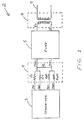
- FIG. 1 shows a block diagram that illustrates a commonly utilized circuit 2 for resistively combining and filtering the input data signals TX+, TX-, TXd+, and TXd-.
- a transmission stage 3 which is typically packaged as an integrated circuit, drives the input data signals TX+, TX-, TXd+, and TXd- onto an external summing resistor network 4 as square-wave current signals.
- the external summing resistor network 4 includes an input resistor Rt, a complementary input resistor Rct, a delayed input resistor Rdt, a complementary delayed input resistor Rcdt, and a balancing resistor Rb.
- the summing resistor network 4 generates both a square-wave transmit voltage signal TXO+ and a square-wave complementary transmit voltage signal TXO- by summing together the voltages generated by driving the input data signal TX+ and the complementary delayed input data signal TXd- across the input resistor Rt and the complementary delayed resistor Rcdt, respectively, and by summing together the voltages generated by driving the complementary input data signal TX- and the delayed input data signal TXd+ across the complementary input resistor Rct and the delayed input resistor Rdt, respectively.
- An external filter 5 which is typically implemented as a conventional low-pass L-C filter, generates the output data signal V+ and a complementary output data signal V- by attenuating the harmonic components of both the square-wave transmit voltage signal TXO+ and the square-wave complementary transmit voltage signal TXO-.
- the output data signal V+ and the complementary output data signal V- are then fed into an external 2:1 transformer 6, which isolates the preceding circuitry 3, 4, and 5 from a twisted-pair cable 7, to generate a transmitted waveform Tw on the twisted-pair cable 7.
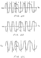
- FIGs. 2A-C show a waveform diagram that illustrates an example of the transmit voltage signal TXO+, the complementary transmit voltage signal TXO-, and the transmitted waveform Tw.
- the transmit voltage signal TXO+ and the complementary transmit voltage signal TXO- are shown as 5 volt peak-to-peak signals centered at Vcc/2.
- the transmitted waveform Tw is shown as a +/- 2.5 volt differential voltage signal in accordance with the twisted-pair specification.
- circuit 2 One problem with utilizing circuit 2 is that since the harmonic components of the square-wave data signals TX+, TX-, TXd+, and TXd- are not attenuated prior to the external filter 5, the data signals TX+, TX-, TXd+, and TXd- radiate a significant amount of harmonic switching noise as a result of the high current levels utilized by the transmission stage 3 to drive the data signals TX+, TX-, TXd+, and TXd-onto the summing resistor network 4. The magnitude of the switching noise typically results in circuit 2 failing to satisfy FCC requirements for radiated emissions.
- circuit 2 Another problem with utilizing circuit 2 is that the external resistor summing network 4 and the external filter 5 consume a substantial area on a circuit board.
- the present invention more particularly provides a waveshaping circuit that transforms an input data signal and a delayed input data signal into a pair of complementary output waveforms, in accordance with the IEEE 802.3 local area network 10BASE-T specification, within a single integrated circuit.
- 10BASE-T transceiver circuitry is provided within a single integrated circuit while the waveshaping function is provided by an external summing resistor network and an external filter.
- a waveshaping circuit which allows the functionality of the summing resistor network 4 and the filter 5 to be integrated with the transmission stage 3 into a single integrated circuit.
- the waveshaping circuit in a practical embodiment transforms the input data signal TX+ and the delayed input data signal TXd+ into the pair of complementary sinusoidal output waveforms V+ and V- by utilizing phase-lock-loop circuitry to produce a plurality of transitions within the pulse widths of the input data signal TX+ and the delayed input data signal TXd+.
- Logic circuitry may be utilized to produce a pair of complementary logic signals in response to each transition or edge, and current source circuitry may be utilized to produce an incremental current in response to each pair of complementary logic signals. By summing together all of the incremental currents, the pair of complementary sinusoidal output waveforms V+ and V- can be formed.
- phase-lock-loop circuitry provides a series of transitions that fall within the pulse widths of the input data signal TX+ and the delayed input data signal TXd+
- phase-lock-loops in general need a relatively large area of a silicon wafer and are subject to varying degrees of instability as a result of transients, temperature variations, and other related conditions.
- Another aspect of the invention concerns a waveshaping circuit that can integrate the functionality of the transmission stage 3, the summing resistor network 4, and the filter 5 into a single integrated circuit, without necessitating the use of phase-lock-loop circuitry.
- the waveshaping circuit includes a frame alignment circuit and a delayed frame alignment circuit.
- the frame alignment circuit generates a phase-adjusted input signal by fixing a phase relationship between an externally-generated input signal, such as the TX+ signal, and an externally-generated oscillator signal.
- the delayed frame alignment circuit generates a phase-adjusted delayed input signal by fixing a phase relationship between an externally-generated delayed input signal, such as the TXd+ signal, and the externally-generated oscillator signal.
- the waveshaping circuit further includes a first input logic stage and a first delayed input logic stage.
- the first input logic stage generates a plurality of pairs of first logic signals so that each pair of first logic signals changes to a first pair of logic states in response to one of the edges of the oscillator signal that follows the leading edge of the phase-adjusted input signal, and changes to a second pair of logic states in response to one of the edges of the oscillator signal that follows the trailing edge of the phase-adjusted input signal.
- the first delayed input logic stage generates a plurality of pairs of first delayed logic signals so that each pair of first delayed logic signals changes to a first pair of logic states in response to one of the edges of the oscillator signal that follows the leading edge of the phase-adjusted delayed input signal, and changes to a second pair of logic states in response to one of the edges of the oscillator signal that follows the trailing edge of the phase-adjusted delayed input signal.
- Each pair of first delayed logic signals corresponds to one pair of first logic signals.
- the waveshaping circuit also includes a weighted current sum stage that generates an output data signal and a complementary output data signal in response to the logic states of both the plurality of pairs of first logic signals and the plurality of pairs of first delayed logic signals.
- each pair of first logic signals and its corresponding pair of first delayed logic signals simultaneously generate both an incremental portion of the output data signal and an incremental portion of the complementary output data signal so that an instantaneous value of the output data signal is determined by summing together the incremental portions of the output data signal, and so that an instantaneous value of the complementary output data signal is determined by summing together the incremental portions of the complementary output data signal.
- the waveshaping circuit can also include a second input logic stage and a second delayed input logic stage.
- the second input logic stage and the second delayed input logic stage provide a greater resolution by utilizing a delayed oscillator signal.
- the second input logic stage generates a plurality of pairs of second logic signals so that each pair of second logic signals changes to a first pair of logic states in response to one of the edges of the delayed oscillator signal that follows the leading edge of the phase-adjusted input signal, and changes to a second pair of logic states in response to one of the edges of the delayed oscillator signal that follows the trailing edge of the phase-adjusted input signal.
- the second delayed input logic stage generates a plurality of pairs of second delayed logic signals so that each pair of second delayed logic signals changes to a first pair of logic states in response to one of the edges of a delayed oscillator signal that follows the leading edge of the phase-adjusted delayed input signal, and changes to a second pair of logic states in response to one of the edges of the delayed oscillator signal that follows the trailing edge of the phase-adjusted delayed input signal.
- each pair of second delayed logic signals corresponds to one pair of second logic signals.
- the weighted current sum stage When the second input logic stage and the second delayed logic stage are utilized, the weighted current sum stage generates an output data signal and a complementary output data signal in response to the logic states of the plurality of pairs of first logic signals, the plurality of pairs of second logic signals, the plurality of pairs of first delayed logic signals, and the plurality of pairs of second delayed logic signals.
- the logic states of each pair of first logic signals and its corresponding pair of first delayed logic signals, and the logic states of each pair of second logic signals and its corresponding pair of second delayed logic signals simultaneously generate both an incremental portion of the output data signal and an incremental portion of the complementary output data signal so that an instantaneous value of the output data signal is determined by summing together the incremental portions of the output data signal, and so that an instantaneous value of the complementary output data signal is determined by summing together the incremental portions of the complementary output data signal.
- the frame alignment circuit can include, for example, a first latch, a delay line, a first delay circuit, a second delay circuit, and a second latch.
- the first latch generates a reset signal by latching a first reset logic state in response to the leading edge of the input signal, and by changing to a second reset logic state when a delayed stop signal is in a second delayed stop logic state.
- the delay line generates a start frame signal with a first start logic state, and a stop frame signal with a first stop logic state when the reset signal is in the second reset logic state, changes the logic state of the start frame signal to a second start logic state in response to a first predetermined edge of the oscillator signal that occurs after the leading edge of the input signal, and changes the logic state of the stop frame signal to a second stop logic state in response to a second predetermined edge of the oscillator signal.
- the first delay circuit generates a delayed start signal by transitioning to a first delayed start logic state a first delay time after the start signal transitions to the first start logic state, and by transitioning to a second delayed start logic state the first delay time after the start signal transitions to the second start logic state.
- the second delay circuit generates the delayed stop signal by transitioning to a first delayed stop logic state a second delay time after the stop signal transitions to the first stop logic state, and by transitioning to the second delayed stop logic state the second delay time after the stop signal transitions to the second stop logic state.
- the second latch generates the phase-adjusted input signal by latching a first phase logic state when the delayed start signal transitions to the second delayed start logic state, and by changing to a second phase logic state when the delayed stop signal transitions to the second delayed stop logic state.
- the input logic stage can be implemented by a plurality of serially-connected latches that are configured so that a data input of the first latch of the series is connected to the phase-adjusted input signal, so that a data input of each remaining latch in the series is connected to a non-inverting output of the preceding latch in the series, so that the oscillator signal is connected to a clock input of each even-numbered latch in the series, and so that an inverted oscillator signal is connected to a clock input each odd-numbered latch in the series.
- the weighted current sum stage can include, for example an output node, a complementary output node, an output resistor connected between a power supply and the output node, a complementary output resistor connected between the power supply and the complementary output node, an output capacitor connected between the output node and ground, and a complementary output capacitor connected between the complementary output node and ground.
- the weighted current sum stage can further include a plurality of first current stages and a plurality of second current stages.
- the plurality of first current stages can be implemented so that each first current stage has a first transistor connected to the output node, a first current node, and one of the logic signals of one of the pairs of logic signals; a second transistor connected to the complementary output node, the first current node, and the remaining logic signal of the one of the pairs of logic signals; and a first current source connected between the first current node and ground.
- each second current stage has a first transistor connected to the output node, a second current node, and one of the logic signals of one of the pairs of delayed logic signals; a second transistor connected to the complementary output node, the second current node, and the remaining logic signal of the one of the pairs of delayed logic signals; and a second current source connected between the second current node and ground.
- the weighted current sum stage can additionally include a third current source connected between the output resistor and ground, and a fourth current source connected between the complementary output resistor and ground.
- FIG. 1 is a block diagram illustrating a commonly utilized circuit 2 for resistively combining and filtering the input data signals TX+, TX-, TXd+, and TXd-.
- FIGs. 2A-C are a waveform diagram illustrating an example of the transmit voltage signal TXO+, the complementary transmit voltage signal TXO-, and the transmitted waveform Tw.
- FIG. 3 is a block diagram illustrating an embodiment of a waveshaping circuit 10.
- FIG. 4 is a block diagram illustrating an embodiment of a phase-lock-loop 12.
- FIG. 5 is a block diagram illustrating an embodiment of an input logic stage 14.
- FIG. 6 is a block diagram illustrating an embodiment of a delayed input logic stage 16.
- FIG. 7 is a schematic diagram illustrating an embodiment of a weighted current sum stage 18.
- FIG. 8 is a timing diagram illustrating the input data signal TXO+, the first logic signal Q1, the first delayed logic signal Qd1, and the first complementary delayed logic signal NQd1.
- FIGs. 9A and 9B are a graphical representation illustrating the conceptual operation of weighted current sum stage 18.
- FIG. 9A shows an example of the input data signal TXO+ which has been divided into a first propagation delay period through a twelfth propagation delay period.
- FIG. 9B shows a resulting sine wave 68 which is created by incrementally adding and subtracting the first through the nth incremental data currents.
- FIG. 10 is a block diagram illustrating a waveshaping circuit 100 in accordance with the first alternative embodiment.
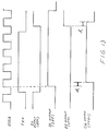
- FIG. 11 is a timing diagram illustrating the operation of frame alignment circuit 110.
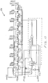
- FIG. 12 is a schematic diagram illustrating frame alignment circuit 110.
- FIG. 13 is a timing diagram illustrating the operation of frame alignment circuit 110.
- FIG. 14 is a block diagram illustrating delayed frame alignment circuit 120.
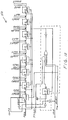
- FIG. 15 is a schematic diagram illustrating first input logic stage 130.
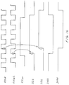
- FIG. 16 is a timing diagram illustrating the operation of first input logic stage 130.
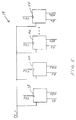
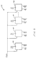
- FIGs. 17, 18, and 19 are block diagrams illustrating second input logic stage 140, first delayed input logic stage 150, and second delayed input logic stage 160.
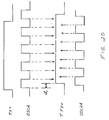
- FIG. 20 is a timing diagram illustrating the use of a delayed oscillator signal OSC2d.
- FIG. 21 is a block diagram illustrating weighted current sum stage 170.
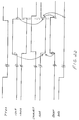
- FIG. 22 is a timing diagram illustrating the operation of low power circuit 190.
- FIG. 3 shows a block diagram that illustrates an embodiment of a waveshaping circuit 10.
- waveshaping circuit 10 transforms an input data signal TX+ and a delayed input data signal TXd+ into a pair of complementary sinusoidal output waveforms V+ and V-, as defined by the IEEE 802.3 local area network 10BASE-T specification, without the use of external components.
- Waveshaping circuit 10 can eliminate the need for external waveshaping components by utilizing phase-lock-loop circuitry to produce a plurality of edges within the pulse widths of the input data signal TX+ and the delayed input data signal TXd+, logic circuitry to produce a pair of complementary logic signals in response to each edge, and current source circuitry to produce an incremental current in response to each pair of complementary logic signals.
- a sinusoidal waveform can be generated by periodically adding and subtracting each incremental current to the total current, which is then sunk to ground through a resistive load.
- waveshaping circuit 10 includes a phase-lock-loop stage 12 that generates a series of incrementally-delayed timing signals TS1-TSn in response to an externally provided oscillator signal OSC, an input logic stage 14 that generates a series of pairs of complementary logic signals Q1/NQ1-Qn/NQn in response to the series of timing signals TS1-TSn and the input data signal TX+, a delayed input logic stage 16 that generates a series of pairs of complementary delayed logic signals Qd1/NQd1-Qdn/NQdn in response to the series of timing signals TS1-TSn and the delayed input data signal TXd+, and a weighted current sum stage 18 that generates the output data signal V+ and the complementary output data signal V- in response to both the series of pairs of complementary logic signals Q1/NQ1-Qn/NQn and the series of pairs of complementary delayed logic signals Qd1/NQd1-Qdn/NQdn.
- FIG. 4 shows a block diagram that illustrates an embodiment of phase-lock-loop stage 12.
- phase-lock-loop stage 12 includes an inverter substage 20 that generates the series of incrementally-delayed timing signals TS1-TSn in response to the oscillator signal OSC and a control voltage Vc, an oscillator inverter 22 that generates an inverted oscillator signal IOSC, a phase comparator 24 that generates an error signal Es in response to a difference between the inverted oscillator signal IOSC and the nth timing signal TSn where the nth timing signal TSn represents the total number of timing signals generated by phase-lock-loop 12, and a charge pump 26 that generates the control voltage Vc in response to the error signal Es.
- inverter substage 20 that generates the series of incrementally-delayed timing signals TS1-TSn in response to the oscillator signal OSC and a control voltage Vc
- an oscillator inverter 22 that generates an inverted oscillator signal IOSC
- a phase comparator 24 that generates an error signal Es in response to a difference between
- Inverter substage 20 is illustrated in FIG. 4 as a series of inverter gates including a first inverter gate 28, a second inverter gate 30, a third inverter gate 32, and a nth inverter gate 34 where the nth inverter gate 34 corresponds to the nth timing signal TSn.
- first inverter gate 28 generates the first timing signal TS1 in response to the oscillator signal OSC
- second inverter gate 30 generates the second timing signal TS2 in response to the first timing signal TS1
- third inverter gate 32 generates the third timing signal TS3 in response to the second timing signal TS2.
- the nth inverter gate 34 generates the nth timing signal TSn in response to a preceding timing signal TSp.
- the first timing signal TS1 and each succeeding odd-numbered timing signal are equivalent to a time delayed inverse of the oscillator signal OSC where the time delay Td of each timing signal TS1-TSn is equivalent to the propagation delay introduced by each preceding inverter gate.
- the propagation delay of each inverter gate 28, 30, 32, and 34 is substantially equivalent.
- the logic state of the oscillator signal OSC changes from a logic low to a logic high
- the logic state of the first timing signal TS1 will change from a logic high to a logic low after the propagation delay introduced by the first inverter gate 28 while the logic state of the third timing signal TS3 will change from a logic high to a logic low after the propagation delay introduced by the first three inverter gates 28, 30, and 32.
- the second timing signal TS2 and each succeeding even-numbered timing signal are equivalent to a time delayed oscillator signal where the time delay Td is defined as above.
- the logic state of the oscillator signal OSC changes from a logic low to a logic high
- the logic state of the second timing signal TS2 will change from a logic low to a logic high after the propagation delay introduced by the first two inverter gates 28 and 30.
- the propagation delay of an inverter gate is a function of the input voltage, the channel width and length of the transistors used to fabricate the inverter gate, and the fabrication process.
- the propagation delay of each inverter gate 28, 30, 32, and 34 will be determined principally by the input voltage.
- each inverter gate 28, 30, 32, and 34 has an input voltage terminal 36 which is connected to the control voltage Vc.
- the control voltage Vc sets an equivalent propagation delay across each of the inverter gates 28, 30, 32, and 34.
- the control voltage Vc is controlled by the feedback action of oscillator inverter 22, phase comparator 24, and charge pump 26 so that the delay time Td of the nth timing signal is approximately one half of the period of the oscillator signal OSC.
- phase comparator 24 receives the inverted oscillator signal IOSC from oscillator inverter 22 and the nth timing signal TSn from the nth inverter gate 34, compares the two signals, and generates an error Es in response to a difference between the two signals.
- Charge pump 24 responds to the error signal Es by either increasing or decreasing the control voltage Vc.
- the requirement for oscillator inverter 22 is dependent on whether the nth inverter gate 34 is an odd-numbered or an even-numbered inverter gate.
- the nth timing signal TSn will transition from a logic low to a logic high when the nth inverter gate 34 is even-numbered and will transition from a logic high to a logic low when the nth inverter gate 34 is odd-numbered.
- the oscillator signal OSC in order to compare the falling edge of the oscillator signal OSC to the rising edge of an even-numbered nth timing signal TSn, the oscillator signal OSC must be inverted.
- 12 inverter gates are utilized.
- phase comparator 24 By utilizing the feedback action of oscillator inverter 22, phase comparator 24, and charge pump 26 to generate a total propagation delay which is approximately one-half of the period of the oscillator signal OSC, a precise propagation delay, which is equivalent to the total number of inverter gates divided by one-half the period of the oscillator signal OSC, is generated.
- waveshaping circuit 10 generates the output data signal V+ and the complementary output data signal V- in response to both the input data signal TX+ and the delayed input data signal TXd+ in accordance with the twisted-pair specification of the IEEE 802.3 local area network standard.
- the input data signal TX+ is defined as a 10 MHz (megahertz) Manchester-encoded signal.
- the delayed input data signal TXd+ is defined as a delayed 10 MHz Manchester-encoded signal where the delay is equivalent to one-half the period of the input data signal TX+ or 50 ns (nanoseconds).
- a signal which is equivalent and synchronized to the input data signal TX+ is utilized as the oscillator signal OSC.
- a propagation delay of 4.167 ns results from dividing the 12 inverter gates of the preferred embodiment by the 50 ns one-half period of the oscillator signal OSC.
- FIG. 5 shows a block diagram that illustrates an embodiment of input logic stage 14.
- input logic stage 14 generates the series of pairs of complementary logic signals Q1/NQ1-Qn/NQn in response to the series of timing signals TS1-TSn and the input data signal TX+.
- Each timing signal TS1-TSn generates one corresponding pair of complementary logic signals by periodically latching the input data signal TX+ so that the logic state and an inverse logic state of the input data signal TX+ are simultaneously provided by the one corresponding pair of complementary logic signals.
- the transmit logic stage is illustrated in FIG. 5 as a series of logic blocks that includes a first logic block 38, a second logic block 40, a third logic block 42, and a nth logic block 44 where the nth logic block 44 corresponds to the nth inverter gate 34. As further shown in FIG. 5 as a series of logic blocks that includes a first logic block 38, a second logic block 40, a third logic block 42, and a nth logic block 44 where the nth logic block 44 corresponds to the nth inverter gate 34. As further shown in FIG.
- first logic block 38 generates the first logic signal Q1 and the first complementary logic signal NQ1 in response to both the input data signal TX+ and the first timing signal TS1
- second logic block 40 generates the second logic signal Q2 and the second complementary logic signal NQ2 in response to both the input data signal TX+ and the second timing signal TS2
- third logic block 42 generates the third transmit logic signal Q3 and the third complementary transmit logic signal NQ3 in response to both the input data signal TX+ and the third timing signal TS3.
- the nth logic block 44 generates the nth transmit logic signal Qn and the nth complementary transmit logic signal NQn in response to both the input data signal TX+ and the nth timing signal TSn.
- the logic blocks 38, 40, 42, and 44 are configured so that each of the logic signals Q1-Qn is equivalent to the period and logic state of the input data signal TX+ that exists when the logic state of each corresponding timing signal TS1-TSn transitions either from a logic low to a logic high or from a logic high to a logic low.
- the logic state of the input data signal TX+ is high when the first timing signal TS1 transitions either from a logic low to a logic high or from a logic low to a logic high, the logic state of the first logic signal Q1 will also be high.
- the complementary logic signals NQ1-NQn are equivalent to the period and the inverse of the logic state of the input data signal TX+ that exists when the logic state of each corresponding timing signal TS1-TSn transitions either from a logic low to a logic high or from a logic high to a logic low.
- the oscillator signal OSC is synchronized to the input data signal TX+, when the logic state of the input data signal TX+ transitions from a logic low to a logic high, the logic state of the first timing signal TS1 will transition from a logic high to a logic low and the first logic signal Q1 will transition from a logic low to a logic high after a delay principally introduced by the first inverter gate 28 (see FIG. 4).
- the logic state of the second timing signal TS2 and the second logic signal Q2 will transition from a logic low to a logic high after a delay principally introduced by the first two inverter gates 28 and 30 (see FIG. 4).
- each logic signal Q1-Qn will transition to a logic high and each complementary logic signal NQ1-NQn will transition to a logic low after the delay time associated with its corresponding inverter gate.
- FIG. 6 shows a block diagram that illustrates an embodiment of the delayed input logic stage 16.
- delayed input logic stage 16 which includes a series of delayed logic blocks including a first delayed logic block 46, a second delayed logic block 48, a third delayed logic block 50, and an nth delayed logic block 52, is substantially identical to the configuration of input logic stage 14 as shown in FIG. 5.
- the only difference between the logic stage 14 and delayed input logic stage 16 is that the series of pairs of complementary delayed logic signals Qd1/NQd1-Qdn/NQdn are generated in response to the series of timing signals TS1-TSn, respectively, and the delayed input data signal TXd+.
- the logic blocks 46, 48, 50, and 52 are configured so that each of the delayed input logic signals Qd1-Qdn is equivalent to the logic state of the delayed input data signal TXd+ that exists when the logic state of each corresponding timing signal TS1-TSn transitions either from a logic low to a logic high or from a logic high to a logic low.
- each delayed input logic signal Qd1-Qdn will transition to a logic high and each complementary delayed transmit logic signal NQd1-NQdn will transition to a logic low after both the delay time associated with its corresponding inverter gate and the one-half period delay.
- the series of pairs of complementary delayed logic signals Qd1/NQd1-Qdn-NQdn corresponds to the series of pairs of complementary logic signals Q1/NQ1-Qn/NQn so that each pair of delayed logic signals corresponds to one pair of logic signals.
- FIG. 7 shows a schematic diagram that illustrates an embodiment of the weighted current sum stage 18.
- Weighted current sum stage 18 generates the output data signal V+ and the complementary output data signal V- in response to both the plurality of pairs of complementary logic signals Q1/NQ1-Qn/NQn and the plurality of pairs of complementary delayed logic signals Qd1/NQd1-Qdn-NQdn.
- Each pair of logic signals Q/NQ and its corresponding pair of delayed logic signals Qd/NQd simultaneously generate both an incremental portion of the output data signal V+ and an incremental portion of the complementary output data signal V-.
- the instantaneous value of the output data signal V+ is determined by summing together all the incremental portions of the output data signal V+ while the instantaneous value of the complementary output data signal V- is also determined by summing together all the incremental portions of the complementary output data signal V-.
- Weighted current sum stage 18 is illustrated in FIG. 7 as an output resistor R1 connected between a power supply Vdd and an output node OUT, a complementary output resistor R2 connected between the power supply Vdd and a complementary output node COUT, and a series of current sources including a first current source 54, a second current source 56, and a nth current source 58 where the nth current source corresponds to the nth logic signals Qn, NQn, Qdn, and NQdn.
- Each current source 54, 56, and 58 generates the portion of the output data signal V+ and the portion of the complementary output data signal V- by sinking either one of a plurality of incremental data currents Id1-Idn through the output resistor R1 or one of a plurality of complementary data currents Ic1-Icn through the complementary output resistor R2, respectively.
- the series of incremental data currents Id1-Idn are illustrated in FIG. 7 as a first incremental data current Id1, a second incremental data current Id2, and a nth incremental data current Idn where the nth incremental data current Idn corresponds to the nth current source 58.
- the series of complementary incremental data currents Ic1-Icn are illustrated in FIG. 7 as a first complementary incremental data current Ic1, a second complementary incremental data current Ic2, and a nth complementary incremental data current Icn where the nth complementary incremental data current Icn corresponds to the nth current source 58.
- the first current source 54 sinks either the first incremental data current Id1 or the first complementary incremental data current Ic1
- the second current source 56 sinks either the second incremental data current Id2 or a second complementary incremental data current Ic2
- the nth current source 58 sinks either the nth incremental data current Idn or the nth complementary incremental data current Icn.
- the first current source 54 includes a data differential pair 60 and a delayed differential pair 62.
- Data differential pair 60 sinks either a first portion Id1f of the first incremental data current Id1 or a first portion Ic1f of the first complementary incremental data current Ic1 while delayed differential pair 62 sinks either a remaining portion Id1r of the first incremental data current Id1 or a remaining portion Ic1r of the first complementary incremental data current Ic1.
- First differential pair 60 includes a first n-channel input transistor T1, a first n-channel complementary input transistor T2, and a first tail current transistor T3.
- input transistor T1 has its source connected to ground through first tail current transistor T3, its drain connected to a power supply Vdd through the output resistor R1, and its gate connected to receive the first logic signal Q1.
- Complementary input transistor T2 has its source connected to ground through first tail current transistor T3, its drain connected to the power supply Vdd through the complementary output resistor R2, and its gate connected to receive the first complementary logic signal NQ1.
- First tail current transistor T3 has its source connected to ground and its gate connected to a bandgap reference current Ibg.
- First tail current transistor T3 sinks either the first portion Id1f of the first incremental data current Id1 or the first portion Ic1f of the first complementary incremental data current Ic1.
- First delayed differential pair 62 includes a first n-channel delayed complementary input transistor T4, a first n-channel delayed input transistor T5, and a first delayed tail current transistor T6.
- Delayed complementary input transistor T4 has its source connected to ground through first delayed tail current transistor T6, its drain connected to the power supply Vdd through the output resistor R1, and its gate connected to receive the first delayed complementary logic signal NQd1.
- First delayed input transistor T5 has its source connected to ground through first delayed tail current transistor T6, its drain connected to the power supply Vdd through the complementary output resistor R2, and its gate connected to receive the first delayed logic signal Qd1.
- First delayed tail current transistor T6 has its source connected to ground and its gate connected to the bandgap reference current Ibg.
- First delayed tail current transistor T6 sinks either the remaining portion Id1r of the first incremental data current Id1 or the remaining portion Ic1r of the first complementary incremental data current Ic1. The magnitude of the remaining portions of the incremental currents are approximately one-third the magnitude of the first portions of the incremental currents.
- each logic signal Q1-Qn when the logic state of the input data signal TX+ transitions from a logic low to a logic high, each logic signal Q1-Qn will transition to a logic high and each complementary logic signal NQ1-NQn will transition to a logic low after the delay time associated with its corresponding inverter gate and each delayed logic signal Qd1-Qdn will transition to a logic high and each complementary delayed logic signal NQd1-NQdn will transition to a logic low after both the delay time associated with its corresponding inverter gate and the one-half period delay.
- the gate-to-source voltage of input transistor T1 increases while the gate-to-source voltage of complementary input transistor T2 simultaneously decreases.
- input transistor T1 begins sinking the first portion Id1f of the first incremental data current Id1 while the complementary input transistor T2 stops sinking the first portion Ic1f of the first complementary incremental data current Ic1.
- the gate-to-source voltage of delayed input transistor T4 increases while the gate-to-source voltage of complementary delayed input transistor T5 simultaneously decreases.
- delayed input transistor T4 begins sinking the remaining portion Id1r of the first incremental data current Id1 while complementary delayed input transistor T5 stops sinking the remaining portion Ic1f of the first complementary incremental data current Ic1.
- second current source 56 and the nth current source 58 both of which are configured as first current source 54, begin sinking the second incremental data current Id2 and the nth incremental data current Idn, respectively, through the output resistor R1 and stop sinking the second complementary incremental data current Ic2 and the nth complementary data current Icn, respectively, through the complementary output resistor R2 in response to their corresponding logic signals Q2/NQ2-Qn/NQn.
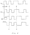
- FIG. 8 shows a timing diagram that illustrates the input data signal TX+, the first logic signal Q1, the first delayed logic signal Qd1, and the first complementary delayed logic signal NQd1.
- the first logic signal Q1 is delayed by a first propagation delay time Pd introduced by the first inverter gate 28 (see FIG. 4) while the first delayed logic signal Qd1 and the complementary delayed transmit logic signal NQd1 are delayed by the first propagation delay time Pd and the one-half period delay Ph.
- both input transistor T1 and delayed input transistor T4 turn on to sink both the first portion Id1f and the remaining portion Id1r of the first incremental data current Id1.
- the logic state of the first complementary delayed logic signal NQd1 transitions from a logic high to a logic low while the logic state of the first logic signal Q1 remains high.
- input transistor T1 remains on while delayed input transistor T4 turns off.
- a defined amplitude step (see FIGS. 2A-C) is formed in accordance with the IEEE 802.3 specification.
- FIGs. 9A and 9B graphically show an example of the operation of current summing stage 18 based on one half the number of incremental currents and propagation delay periods as utilized in the preferred embodiment.
- FIG. 9A shows an example of one period of the input data signal TX+ which has been divided into twelve propagation delay periods Pd1-Pd12. As derived from the above, the twelve propagation delay periods Pd1-Pd12 result from utilizing six inverter gates generating 24 transmit logic signals to 6 logic blocks which generate 6 incremental data currents Id1-Id6 and 6 incremental complementary data currents Ic1-Ic6.
- FIG. 9B example only the operation of the incremental data currents Id1-Id6 are illustrated.
- FIG. 9B shows a resulting waveform which is created by incrementally adding and subtracting the six incremental data currents Id1-Id6.
- a first incremental data current Id1 represented by one unit of current is generated.
- the first incremental data current Id1 and each of the six succeeding incremental data currents Id2-Id6 are generated for a period of time which is equivalent to one half the period of the input data signal TX+.
- a second incremental data current Id2 represented by two additional units of additional current is generated. As is graphically depicted in FIG. 9B, the second incremental data current Id2 is added to the first incremental data current Id1. Thus, after the second propagation delay period Pd2, the total data current is represented by three units of current.
- a third incremental data current Id3 represented by three additional units of current are generated and added to the previous units of current.
- the total data current is represented by six units of current.
- a fourth propagation delay period Pd4 a fifth propagation delay period Pd5, and a sixth propagation delay period Pd5
- a fourth, a fifth, and a sixth incremental data currents Id4, Id5, and Id6, respectively are generated.
- the fourth, the fifth, and the sixth incremental data currents Id4, Id5, and Id6, which are represented by three additional units, two additional units, and one additional unit of current, respectively, are added to the previous units of current.
- the total data current is represented by 12 units of current. Therefore, by adding the incremental units of current together, the rising edge 66 of a stepped sine wave 68 is formed.
- the first incremental data current Id1 is terminated and subtracted from the total data current.
- the total data current is represented by 11 units of current.
- the second incremental data current Id2 is terminated and subtracted from the total data current.
- the total data current is represented by 9 units of current. Therefore, as can be seen in FIG. 9B, a falling edge 70 of the stepped sine wave 68 is formed from the termination of each incremental data current.
- Testing of weighted current sum stage 18 indicates that a minimum of eight incremental currents and sixteen propagation delay periods are required to define the resulting sine wave in accordance with the IEEE 802.3 standard. In the preferred embodiment, 12 incremental currents and 24 propagation delay periods are utilized.
- the output capacitor C1 and the complementary output capacitor C2 both of which function as low-pass filters, smooth out the stepped sine wave 68 to produce the output data signal V+ and the complementary output data signal V-.
- the waveshaping circuit 10 transforms the input data signal TX+ and the delayed input data signal TXd+ into a pair of complementary sinusoidal output waveforms V+ and V-, as defined by the IEEE 802.3 local area network 10BASE-T specification, without the use of external waveshaping components. As a result, the size, cost, emissions, and complexity of a 10BASE-T installation can be reduced.
- phase-lock-loop circuitry provides a series of edges that fall within the pulse widths of the input data signal TX+ and the delayed input data signal TXd+
- phase-lock-loops in general require a relatively large area and are subject to varying degrees of instability as a result of transients, temperature variations, and other related conditions.
- the edges of an oscillator signal can be utilized as the series of edges. As a result, the need for a phase-lock-loop can be eliminated.
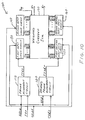
- FIG. 10 shows a block diagram of a waveshaping circuit 100.
- waveshaping circuit 100 includes a frame alignment circuit 110 that generates a phase-adjusted input signal TTX+ by fixing a phase relationship between the input data signal TX+ and an externally-generated oscillator signal OSC2.
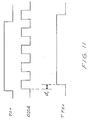
- FIG. 11 shows a timing diagram which illustrates the operation of frame alignment circuit 110.
- the period of the oscillator signal OSC2 is set to be a multiple of the period of the input data signal TX+.
- a defined number of oscillator periods equal the period of the input data signal TX+.
- the oscillator signal OSC2 is implemented as an 80 MHz oscillator signal.
- four 12.5 nS clock periods can be fit within one-half of the period of the input data signal TX+ which, as stated above, is 50nS.
- a total of eight edges can be generated within the pulse width.
- other variations of the delay time d1 and the period of the oscillator signal OSC2 can be used to generate a greater or lesser number of edges within the pulse width of the input data signal TX+.
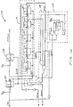
- FIG. 12 shows a schematic diagram that illustrates frame alignment circuit 110.
- frame alignment circuit 110 includes a D latch D0 that latches a logic low at its inverting output as a reset signal RST in response to the rising edge of the input data signal TX+, and that resets the reset signal RST to a logic high in response to the rising edge of a delayed stop signal DSTP.
- Frame alignment circuit 110 also includes a delay line 114 that generates a start frame signal SRT with a low logic state and a stop frame signal STP with low logic state when the reset signal RST is a logic high, that changes the logic state of the start frame signal SRT to a logic high in response to the first rising edge of the oscillator signal OSC2 that occurs after the rising edge of the input data signal TX+, and that changes the logic state of the stop frame signal STP to a logic high in response to the fifth rising edge of the oscillator signal OSC2.
- delay line 114 includes five D latches D1-D5 which are connected together in a feedback configuration so that the D input of latch D1 is connected to the inverting output of latch D5, and so that the D-inputs of latches D2-D5 are connected to the non-inverting outputs of latches D1-D4, respectively.
- the reset inputs and the clock inputs of each of the latches D1-D5 are connected to the reset signal RST and the oscillator signal OSC2, respectively.
- Frame alignment circuit 110 also includes a delay circuit 116 that delays the start signal SRT a first delay time to generate a delayed start signal DSRT.
- a delay circuit 116 that delays the start signal SRT a first delay time to generate a delayed start signal DSRT.
- frame alignment circuit 110 also includes a delay circuit 118 that generates the delayed stop signal DSTP by delaying the stop signal STP a second delay time.
- a delay circuit 118 that generates the delayed stop signal DSTP by delaying the stop signal STP a second delay time.
- frame alignment circuit 110 includes a D latch D6 that latches a logic high at its non-inverting output to produce the rising edge of the phase-adjusted input signal TTX+ in response to the rising edge of the delayed start signal DSRT, and that resets the non-inverting output to a logic low to produce the falling edge of the phase-adjusted input signal TTX+ in response to the rising edge of the delayed stop signal DSTP.
- D latch D6 that latches a logic high at its non-inverting output to produce the rising edge of the phase-adjusted input signal TTX+ in response to the rising edge of the delayed start signal DSRT, and that resets the non-inverting output to a logic low to produce the falling edge of the phase-adjusted input signal TTX+ in response to the rising edge of the delayed stop signal DSTP.
- FIG. 13 shows a timing diagram that illustrates the operation of frame alignment circuit 110.
- the reset signal RST transitions to a logic low, thereby releasing latches D1-D5 from the reset condition.
- a logic low is present at the non-inverting outputs of latches D1-D5, including the start signal SRT, which is taken from the non-inverting output of latch D1, and the stop signal STP, which is taken from the non-inverting output of latch D5.
- the start signal SRT is clocked from a logic low to a logic high in response to the rising edge of the first oscillator signal OSC2 that occurs after the rising edge of the input data signal TX+.
- the phase-adjusted input signal TTX+ transitions to a logic high a first delay time d1 later.
- waveshaping circuit 100 also includes a delayed frame alignment circuit 120 that generates a phase-adjusted delayed input signal TTXd+ by fixing a phase relationship between the delayed input signal TXd+ and the oscillator signal OSC2.
- FIG. 14 shows a block diagram that illustrates delayed frame alignment circuit 120. As can be seen in FIG. 14, delayed frame alignment circuit 120 is identical to frame alignment circuit 110 and therefore operates as described above.
- Waveshaping circuit 100 also includes a first input logic stage 130 that generates a series of pairs of logic signals 1Q1/1NQ1-1Q8/1NQ8 so that each pair of logic signals Q/NQ changes to a first pair of logic states in response to one of the edges of the oscillator signal OSC2 that follows the leading edge of the phase-adjusted input signal TTX+, and changes to a second pair of logic states in response to one of the edges of the oscillator signal OSC2 that follows the trailing edge of the phase-adjusted input signal TTX+.
- FIG. 15 shows a schematic diagram that illustrates first input logic stage 130.
- first input logic stage 130 includes eight D-latches D11-D18 which are connected together in a shift-right configuration so that the D-input of latch D11 is connected to the phase-adjusted input signal TTX+, and so that the non-inverting outputs of latches D11-D17 are connected to the D-inputs of latches D12-D18, respectively.
- FIG. 16 shows a timing diagram that illustrates the operation of first input logic stage 130.
- the logic signal 1Q1 transitions to a logic high while the logic signal 1NQ1 transitions to a logic low in response to the first rising edge of the inverted oscillator signal OSC2 that follows.
- the logic signal 1Q2 transitions to a logic high while the logic signal 1NQ2 transitions to a logic low in response to the first rising edge of the oscillator signal OSC2 that follows.
- phase-adjusted input signal TTX+ transitions from a logic low to a logic high
- latches D11, D13, D15, and D17 latch a logic high and a logic low as logic signals 1Q1/1NQ1, 1Q3/1NQ3, 1Q5/1NQ5, and 1Q7/1NQ7, respectively, with the first, second, third, and fourth falling edges, respectively, of the oscillator signal OSC2 that follow the transition of the phase shifted input signal TTX+.
- latches D12, D14, D16, and D18 latch a logic high and a logic low as logic signals 1Q2/1NQ2, 1Q4/1NQ4, 1Q6/1NQ6, and 1Q8/1NQ8, respectively, with the first, second, third, and fourth rising edges, respectively, of the oscillator signal OSC2 that follow the transition of the phase-adjusted input signal TTX+.
- waveshaping circuit 100 also includes a second input logic stage 140, a first delayed input logic stage 150, and a second delayed input logic stage 160.
- logic stage 140 generates the series of pairs of complementary logic signals 2Q1/2NQ1-2Q8/2NQ8 in response to the phase-aligned input signal TTX+ and a delayed oscillator signal OSC2d while logic stages 150 and 160 generate the series of pairs of delayed complementary logic signals 1Qd1/1NQd1-1Qd8/1NQd8 and 2Qd1/2NQd1-2Qd8/2NQd8, respectively, in response to the oscillator signal OSC2 and the delayed oscillator signal OSC2d, respectively, and the delayed phase-aligned input signal TTXd+.
- each pair of logic signals Q/NQ within the first series of pairs of logic signals 1Q1/1NQ1-1Q8/1NQ8 corresponds with one pair of logic signals within the first series of pairs of logic signals 1Qd1/1NQd1-1Qd8/1NQd8.
- each pair of logic signals Q/NQ within the second series of pairs of logic signals 2Q1/2NQ1-2Q8/2NQ8 corresponds with one pair of logic signals within the second series of pairs of logic signals 2Qd1/2NQd1-2Qd8/2NQd8.
- FIGs. 17, 18, and 19 show a block diagram that illustrates second input logic stage 140, first delayed input logic stage 150, and second delayed input logic stage 160.
- second input logic stage 140, first delayed input logic stage 150, and second delayed input logic stage 160 are identical to first input logic stage 130 and therefore operate as described above.
- FIG. 20 shows a timing diagram that illustrates the use of a delayed oscillator signal OSC2d.
- the delayed oscillator signal OSC2d by using the delayed oscillator signal OSC2d in addition to oscillator signal OSC2, an additional eight edges can be generated within the pulse width of the input data signal TX+, thereby improving the resolution of the output waveforms V+ and V-.
- the rising edge of the delayed oscillator signal OSC2d is delayed ___ nS from the rising edge of the oscillator signal OSC2.
- waveshaping circuit 100 utilizes second input logic stage 140 and second delayed input logic stage 160 to provide an additional eight edges within the pulse widths of the input data signal TX+ and the delayed input data signal TXd+, waveshaping circuit 100 can also function without the use of second input logic stage 140 and second delayed input logic stage 160.
- waveshaping circuit 100 further includes a weighted current sum stage 170 that generates the pair of complementary output waveforms V+ and V- in response to the plurality of pairs of complementary logic signals 1Q1/1NQ1-1Q8/1NQ8, 2Q1/2NQ1-2Q8/2NQ8, 1Qd1/1NQd1-1Qd8-1NQd8 and 2Qd1/2NQd1-2Qd8-2NQd8.
- a weighted current sum stage 170 that generates the pair of complementary output waveforms V+ and V- in response to the plurality of pairs of complementary logic signals 1Q1/1NQ1-1Q8/1NQ8, 2Q1/2NQ1-2Q8/2NQ8, 1Qd1/1NQd1-1Qd8-1NQd8 and 2Qd1/2NQd1-2Qd8-2NQd8.
- FIG. 21 shows a block diagram that illustrates weighted current sum stage 170.
- weighted current sum stage 170 is identical to weighted current sum stage 18 of FIG. 7, e.g., one current source corresponds to each pair of logic signals, and therefore operates as described above.
- each pair of logic signals Q/NQ and its corresponding pair of delayed logic signals Qd/NQd simultaneously generate both an incremental portion of the output waveform V+ and an incremental portion of the output waveform V- by generating incremental currents.
- the instantaneous value of the output waveform V+ is determined by summing together all the incremental portions of the output waveform V+ while the instantaneous value of the output waveform V- is also determined by summing together all the incremental portions of the output waveform V-.
- weighted current sum stage 170 also includes a pair of bias current sources IB1 and IB2 that establish a bias voltage at nodes OUT and COUT when no other current is present. As shown in FIG. 21, current source IB1 is connected between output resistor R1 and output capacitor C1 while current source IB2 is connected between complementary output resistor R1 and complementary output capacitor C2.
- the voltage difference between the pair of complementary output waveforms V+ and V- should ideally be equal. Since the instantaneous value of the pair of output waveforms V+ and V- is determined by summing together all of the incremental portions of the pair of output waveforms V+ and V-, the greatest power savings can be achieved when the sum total of the incremental portions is zero.
- One technique for obtaining a zero sum total is to control the logic states of the plurality of pairs of complementary logic signals 1Q1/1NQ1-1Q8/1NQ8, 2Q1/2NQ1-2Q8/2NQ8, 1Qd1/1NQd1-1Qd8-1NQd8, and 2Qd1/2NQd1-2Qd8-2NQd8. For example if logic signals 1Q1/1NQ5-1Q4/1NQ8 are set to a logic high while logic signals 1Q5/1NQ1-1Q8/1NQ4 are set to a logic low, then by summing together all of the incremental portions a total voltage of zero can be achieved.
- first input logic stage 130 also includes a low power circuit 190 that sets the logic states of each pair Q/NQ of first logic signals 1Q1/1NQ1-1Q8/1NQ8 so that one group of first logic signals is set to one pair of logic states, and so that a second group of first logic signals is set to an opposite pair of logic states when the phase-adjusted input signal TTX+ is undetected for the predetermined period of time.
- a low power circuit 190 sets the logic states of each pair Q/NQ of first logic signals 1Q1/1NQ1-1Q8/1NQ8 so that one group of first logic signals is set to one pair of logic states, and so that a second group of first logic signals is set to an opposite pair of logic states when the phase-adjusted input signal TTX+ is undetected for the predetermined period of time.
- low power circuit 190 includes an inverter INV1 that transmits a local reset signal LOCALRST with a logic state that is inverted from the logic state of a NOR signal NOR to the reset input of latches D12-D18.
- a NOR gate N1 generates the NOR signal NOR in response to the logic states of an AND signal AND, an externally-generated idle signal IDLE, which indicates that no transmission activity has occurred for a predetermined period of time, and an externally-generated reset signal RESET.
- the reset signal RESET is connected to the reset input of latch D11.
- Low power circuit 190 also includes an AND gate AN1 that generates the AND signal AND in response to the logic state of a latch signal LAT and the phase-adjusted input signal TTX+, and a D latch D20 that generates the latch signal LAT as a logic high in response to the falling edge of the oscillator signal OSC2.
- an inverter INV2 transmits an inverted idle signal IDLEZ with a logic state that is inverted from the logic state of the idle signal IDLE, to the set input of latches D11-D14.
- FIG. 22 shows a timing diagram that illustrates the operation of low power circuit 190.
- the idle signal IDLE and the reset signal RESET transition to a logic high.
- the inverted idle signal IDLEZ transitions to a logic low, thereby setting the non-inverting outputs of latches D11-D14 to a logic high while setting the inverting outputs of latches D11-D14 to a logic low.
- the rising edge of the idle signal IDLE and the reset signal RESET cause the NOR gate N1 to generate the NOR signal NOR with a logic low which, one inverter delay later, causes the local reset signal LOGALRST to transition to a logic high, thereby setting the non-inverting outputs of latches D15-D18 to a logic low while setting the inverting outputs of latches D15-D18 to a logic high.
- latches D12-D14 are set priority latches. Therefore, although latches D12-D14 receive both the inverted idle signal IDLEZ and the local reset signal LOCALRST, the inverted idle signal IDLEZ has priority.
- the logic state of the idle signal transitions to a logic low.
- the logic state of the inverted idle signal IDLEZ changes to a logic high.
- a logic low is set at the non-inverting outputs of latches D11-D14 while a logic high is set at the inverting outputs.
- the external reset signal RESET changes to a logic low, thereby allowing latch D1 to latch the phase-adjusted input signal TTX+ at the next edge of the oscillator signal OSC2.
- the reset signal RESET causes the NOR gate N1 to change to a logic high.
- the local reset signal LOCALRST transitions to a logic low, thereby allowing latches D12-D18 to respond to the subsequent edges of the oscillator signal OSC2.
- waveshaping circuit 100 transforms the input data signal TX+ and the delayed input data signal TXd+ into a pair of complementary sinusoidal output waveforms V+ and V-, as defined by the IEEE 802.3 10BASE-T specification, without utilizing a phase-lock-loop and, as above, without the use of external waveshaping components. As a result, the size, cost, and complexity of a 10BASE-T installation can be further reduced.
Landscapes
- Engineering & Computer Science (AREA)
- Power Engineering (AREA)
- Computer Networks & Wireless Communication (AREA)
- Signal Processing (AREA)
- Physics & Mathematics (AREA)
- Spectroscopy & Molecular Physics (AREA)
- Theoretical Computer Science (AREA)
- Manipulation Of Pulses (AREA)
- Dc Digital Transmission (AREA)
- Stabilization Of Oscillater, Synchronisation, Frequency Synthesizers (AREA)
Applications Claiming Priority (4)
| Application Number | Priority Date | Filing Date | Title |
|---|---|---|---|
| US07/994,660 US5357145A (en) | 1992-12-22 | 1992-12-22 | Integrated waveshaping circuit using weighted current summing |
| US133405 | 1993-10-07 | ||
| US08/133,405 US5410188A (en) | 1992-12-22 | 1993-10-07 | Enhanced integrated waveshaping circuit |
| US994660 | 1997-12-19 |
Publications (2)
| Publication Number | Publication Date |
|---|---|
| EP0607677A2 true EP0607677A2 (fr) | 1994-07-27 |
| EP0607677A3 EP0607677A3 (fr) | 1997-09-03 |
Family
ID=26831347
Family Applications (1)
| Application Number | Title | Priority Date | Filing Date |
|---|---|---|---|
| EP93310017A Withdrawn EP0607677A3 (fr) | 1992-12-22 | 1993-12-13 | Circuit intégré de mise en forme d'ondes. |
Country Status (4)
| Country | Link |
|---|---|
| US (1) | US5410188A (fr) |
| EP (1) | EP0607677A3 (fr) |
| JP (1) | JP3515798B2 (fr) |
| KR (1) | KR100282286B1 (fr) |
Cited By (5)
| Publication number | Priority date | Publication date | Assignee | Title |
|---|---|---|---|---|
| WO1999038296A1 (fr) * | 1998-01-21 | 1999-07-29 | Gennum Corporation | Circuit d'attaque de ligne a transitions lineaires |
| EP0673139A3 (fr) * | 1994-03-17 | 1999-11-17 | Advanced Micro Devices, Inc. | Emetteur avec mise en forme d'impulsions précodées |
| WO2000070920A1 (fr) * | 1999-05-17 | 2000-11-23 | Noontek Limited | Circuit de ballast electronique |
| EP0959595A3 (fr) * | 1998-05-18 | 2003-08-06 | Infineon Technologies AG | Dispositif d'émission et système de bus pour transmission de données |
| EP1518323B1 (fr) * | 2002-06-19 | 2006-11-02 | R & C Holding ApS | Boucle a phase asservie a detecteurs de phase incrementaux et convertisseur pour combiner une operation logique et une conversion numerique-analogique |
Families Citing this family (19)
| Publication number | Priority date | Publication date | Assignee | Title |
|---|---|---|---|---|
| US5541957A (en) * | 1994-06-15 | 1996-07-30 | National Semiconductor Corporation | Apparatus for transmitting and/or receiving data at different data transfer rates especially in applications such as dual-rate ethernet local-area networks |
| US5717350A (en) * | 1994-11-09 | 1998-02-10 | Micro Linear Corporation | Degenerated differential pair waveform builder |
| US5651029A (en) * | 1995-05-16 | 1997-07-22 | Myson Technology, Inc. | Apparatus for transmitting an output with predetermined frequency response to an unshielded twisted-pair media and waveform shaping circuit and method employed therein |
| US5822325A (en) * | 1995-07-10 | 1998-10-13 | National Semiconductor Corporation | Integrated twisted pair filter with a secure RIC function |
| US6470405B2 (en) * | 1995-10-19 | 2002-10-22 | Rambus Inc. | Protocol for communication with dynamic memory |
| US5767653A (en) * | 1995-10-24 | 1998-06-16 | Micro Linear Corporation | Variable speed AC induction motor controller |
| US5629641A (en) * | 1996-02-06 | 1997-05-13 | Advanced Micro Devices, Inc. | Differential CMOS current amplifier with controlled bandwidth and common mode distortion |
| US5714897A (en) * | 1996-06-19 | 1998-02-03 | Micro Linear Corporation | Phase-shifted triangle wave generator |
| US5818669A (en) * | 1996-07-30 | 1998-10-06 | Micro Linear Corporation | Zener diode power dissipation limiting circuit |
| US5896015A (en) * | 1996-07-30 | 1999-04-20 | Micro Linear Corporation | Method and circuit for forming pulses centered about zero crossings of a sinusoid |
| US5825223A (en) * | 1996-07-30 | 1998-10-20 | Micro Linear Corporation | Technique for controlling the slope of a periodic waveform |
| US5965989A (en) * | 1996-07-30 | 1999-10-12 | Micro Linear Corporation | Transformer primary side lamp current sense circuit |
| US5793168A (en) * | 1996-08-23 | 1998-08-11 | Micro Linear Corporation | Active deceleration circuit for a brushless DC motor |
| US5896417A (en) * | 1996-10-25 | 1999-04-20 | National Semiconductor Corporation | Apparatus utilizing current-to-voltage conversion for transmitting data at different data transfer rates especially in applications such as dual-rate ethernet local-area networks |
| US5936450A (en) * | 1997-03-21 | 1999-08-10 | National Semiconductor Corporation | Waveshaping circuit using digitally controlled weighted current summing |
| US6266379B1 (en) | 1997-06-20 | 2001-07-24 | Massachusetts Institute Of Technology | Digital transmitter with equalization |
| US5859518A (en) * | 1997-12-22 | 1999-01-12 | Micro Linear Corporation | Switched reluctance motor controller with sensorless rotor position detection |
| US6344980B1 (en) | 1999-01-14 | 2002-02-05 | Fairchild Semiconductor Corporation | Universal pulse width modulating power converter |
| US8188682B2 (en) * | 2006-07-07 | 2012-05-29 | Maxim Integrated Products, Inc. | High current fast rise and fall time LED driver |
Family Cites Families (12)
| Publication number | Priority date | Publication date | Assignee | Title |
|---|---|---|---|---|
| FR1407834A (fr) * | 1964-06-26 | 1965-08-06 | Lignes Telegraph Telephon | Répéteur-régénérateur biternaire |
| US3504290A (en) * | 1967-12-13 | 1970-03-31 | Bell Telephone Labor Inc | Pulse corrector |
| US3659207A (en) * | 1969-10-08 | 1972-04-25 | Xerox Corp | Multi-waveform generation from a single tapped delay line |
| US3612916A (en) * | 1970-07-29 | 1971-10-12 | Daniel R O Neill | Differential phase shifter |
| US3889198A (en) * | 1974-02-22 | 1975-06-10 | Gte Automatic Electric Lab Inc | Voltage waveform generator including feedback arrangement for restoring voltage to initial condition |
| SU1190493A1 (ru) * | 1984-02-16 | 1985-11-07 | Предприятие П/Я Г-4181 | Формирователь бипол рных импульсов |
| DE3418213A1 (de) * | 1984-05-16 | 1985-11-21 | Siemens AG, 1000 Berlin und 8000 München | Entscheiderschaltung |
| CA1242770A (fr) * | 1985-08-06 | 1988-10-04 | Mosaid Technologies Inc. | Generateur de signaux de synchronisation programmable |
| NL8601331A (nl) * | 1986-05-26 | 1987-12-16 | At & T & Philips Telecomm | Zender voor isdn s-bus koppelvlakcircuit. |
| US5134311A (en) * | 1990-06-07 | 1992-07-28 | International Business Machines Corporation | Self-adjusting impedance matching driver |
| US5153466A (en) * | 1991-03-26 | 1992-10-06 | Medtronic, Inc. | All monolithic transceiver operative from a low voltage vcc dc supply |
| US5287386A (en) * | 1991-03-27 | 1994-02-15 | Thinking Machines Corporation | Differential driver/receiver circuit |
-
1993
- 1993-10-07 US US08/133,405 patent/US5410188A/en not_active Expired - Lifetime
- 1993-12-13 EP EP93310017A patent/EP0607677A3/fr not_active Withdrawn
- 1993-12-21 KR KR1019930028759A patent/KR100282286B1/ko not_active Expired - Lifetime
- 1993-12-22 JP JP32373593A patent/JP3515798B2/ja not_active Expired - Lifetime
Cited By (7)
| Publication number | Priority date | Publication date | Assignee | Title |
|---|---|---|---|---|
| EP0673139A3 (fr) * | 1994-03-17 | 1999-11-17 | Advanced Micro Devices, Inc. | Emetteur avec mise en forme d'impulsions précodées |
| WO1999038296A1 (fr) * | 1998-01-21 | 1999-07-29 | Gennum Corporation | Circuit d'attaque de ligne a transitions lineaires |
| US6288592B1 (en) | 1998-01-21 | 2001-09-11 | Gennum Corporation | Cable driver with controlled linear rise and fall |
| EP0959595A3 (fr) * | 1998-05-18 | 2003-08-06 | Infineon Technologies AG | Dispositif d'émission et système de bus pour transmission de données |
| WO2000070920A1 (fr) * | 1999-05-17 | 2000-11-23 | Noontek Limited | Circuit de ballast electronique |
| EP1518323B1 (fr) * | 2002-06-19 | 2006-11-02 | R & C Holding ApS | Boucle a phase asservie a detecteurs de phase incrementaux et convertisseur pour combiner une operation logique et une conversion numerique-analogique |
| US7425851B2 (en) | 2002-06-19 | 2008-09-16 | R & C Holding Aps | Phase-locked loop with incremental phase detectors and a converter for combining a logical operation with a digital to analog conversion |
Also Published As
| Publication number | Publication date |
|---|---|
| KR100282286B1 (ko) | 2001-02-15 |
| JPH077526A (ja) | 1995-01-10 |
| JP3515798B2 (ja) | 2004-04-05 |
| EP0607677A3 (fr) | 1997-09-03 |
| KR940017438A (ko) | 1994-07-26 |
| US5410188A (en) | 1995-04-25 |
Similar Documents
| Publication | Publication Date | Title |
|---|---|---|
| US5410188A (en) | Enhanced integrated waveshaping circuit | |
| US5357145A (en) | Integrated waveshaping circuit using weighted current summing | |
| US5936450A (en) | Waveshaping circuit using digitally controlled weighted current summing | |
| US6011822A (en) | Differential charge pump based phase locked loop or delay locked loop | |
| US6643790B1 (en) | Duty cycle correction circuit with frequency-dependent bias generator | |
| KR100303804B1 (ko) | 클럭지연회로와이를이용한발진회로및위상동기회로 | |
| JP3955150B2 (ja) | 位相インターポレータ、タイミング信号発生回路、および、該タイミング信号発生回路が適用される半導体集積回路装置並びに半導体集積回路システム | |
| US6061418A (en) | Variable clock divider with selectable duty cycle | |
| EP0930714A1 (fr) | Boucle à verrouillage de phase digitale avec diminution de la gigue | |
| EP0608972B1 (fr) | Générateur de signal d'horloge numérique | |
| EP0306662A2 (fr) | Dispositif de génération de signaux destinés à compenser des décalages temporels | |
| US5933037A (en) | High speed phase lock loop having constant bandwidth | |
| US5805089A (en) | Time-division data multiplexer with feedback for clock cross-over adjustment | |
| US6249164B1 (en) | Delay circuit arrangement for use in a DAC/driver waveform generator with phase lock rise time control | |
| US7352755B2 (en) | Network interface card (NIC) with phase lock rise time control generating circuit | |
| JP7514070B2 (ja) | 受信回路並びに受信回路を用いる半導体装置及び半導体システム | |
| CN118842452B (zh) | 一种多相位时钟产生电路及其校准方法 | |
| US20080143318A1 (en) | High frequency delay circuit and test apparatus | |
| EP0556984A1 (fr) | Détecteur de phase | |
| WO1995028032A1 (fr) | Generateur de synchronisation | |
| US7747892B2 (en) | System for automatically selecting intermediate power supply voltages for intermediate level shifters | |
| CN106549668B (zh) | 多模分频器及其基本分频单元 | |
| US20110150159A1 (en) | Clock-forwarding technique for high-speed links | |
| US7342977B2 (en) | Serial data transmitter with bit doubling | |
| US6906564B2 (en) | Apparatus and method for delay matching of full and divided clock signals |
Legal Events
| Date | Code | Title | Description |
|---|---|---|---|
| PUAI | Public reference made under article 153(3) epc to a published international application that has entered the european phase |
Free format text: ORIGINAL CODE: 0009012 |
|
| AK | Designated contracting states |
Kind code of ref document: A2 Designated state(s): DE FR GB IT |
|
| PUAL | Search report despatched |
Free format text: ORIGINAL CODE: 0009013 |
|
| AK | Designated contracting states |
Kind code of ref document: A3 Designated state(s): DE FR GB IT |
|
| STAA | Information on the status of an ep patent application or granted ep patent |
Free format text: STATUS: THE APPLICATION HAS BEEN WITHDRAWN |
|
| 18W | Application withdrawn |
Withdrawal date: 19970913 |